Note: Descriptions are shown in the official language in which they were submitted.
CA 02989406 2017-12-13
WO 2016/204830 PCT/US2016/020406
INTER COUPLING OF MICROINVERTERS
RELATED APPLICATIONS
This application claims priority to US Utility Application Serial Number
14/740972, filed
June 16, 2015, the disclosure of which is incorporated herein by reference in
its entirety.
BACKGROUND
The present invention relates to DC-to-AC convertors for electric power
systems. Lower
cost, high-power, efficient, DC-to-AC convertors are of interest for solar
energy economics. In
the prior art, DC-AC inverters are the second highest cost item next to the
photovoltaic panels.
For high efficiency and low heat dissipation, commutation of DC to produce AC
preferably uses
solid state switches that are either fully on or fully off, and do not dwell
more than a microsecond
or so in an intermediate state. Therefore it is more complicated to produce a
sine wave that
takes on all values between the negative peak and the positive peak. On the
other hand,
producing a square wave which switches between the positive peak and the
negative peak
produces a form of AC that is not suitable for all loads.
Various manufacturers provide prior art DC-AC convertors that fall into one of
a few
broad classes and operating modes. The class of "modified sine wave"
converters maintains
both the same RMS and the same peak voltage as a sine wave, while still
employing only on-off
commutation. This is done by switching the voltage between the desired
positive peak, zero and
the negative peak, spending 50% of the repetition period at zero, therefore
achieving both the
same peak and the same RMS values as a true sine wave, and being compatible
with a greater
variety of loads.
Still, there are loads that do not tolerate the modified sine wave; for
example appliances
that present inductive loads, such as induction motors, some cellphone and
laptop battery
chargers, fluorescent lamps and tumble dryers, and any device with an internal
power supply
that uses capacitive reactance as a lossless voltage-dropping means, can
malfunction on
modified sine waveforms. Moreover, there is a potential problem with radio and
TV interference
due to the high level of harmonics of the modified square wave converter. Such
a waveform is
therefore not a candidate for coupling solar-generated power into the utility
network or into
house wiring.
"True sine wave" is another class of prior art DC-AC converter, and is
required for
coupling power into the grid or into premises wiring.
Another categorization of convertor relates to whether they are designed to
power loads
directly, or whether they are designed to feed and sell power back into the
electricity grid. A load
inverter that can power loads directly is said to operate in standalone mode,
and is also called a
"standalone inverter", while a grid-tie inverter is said to operate in grid-
interactive mode and is
also called a "grid-interactive inverter."
1
CA 02989406 2017-12-13
WO 2016/204830 PCT/US2016/020406
For safety and other reasons, the latter have to meet different specifications
than the
former, especially under fault conditions. In particular, a load inverter
should be a constant
voltage source, while a grid-tie inverter does not have a constant voltage
output but must adapt
to the voltage of the grid, and is rather a controlled current source.
Moreover, a load inverter is
always used with energy storage such as a rechargeable battery, and should
maintain efficiency
at both light and heavy loads and have low, no-load power consumption, so that
the battery is
not discharged while the inverter is idling at night. Grid-tie inverters
however do not have the
same a requirement for no-load power consumption, as they do not operate at
night.
Many prior art inverters used low-frequency transformers in the synthesis of
sine
waveforms, but the large amount of copper and iron required for low-frequency
transformers
adds significant cost and weight.
Transformerless inverters are known in the prior art, particularly for utility-
interactive
inverters, which use high-frequency switching or pulse width modulation to
approximate a sine
wave. However, a disadvantage that arises in certain of these converter
concepts is the
imposition of the high-frequency switching waveform on the solar array, which
can capacitively
couple through the glass cover upon touching it, potentially causing RF burn
to personnel or
damage to the solar panel, as well as causing the solar array to radiate
substantial radio
interference. Thus a design is required that can create a more benign common-
mode voltage
fluctuation on the solar array DC conductors.
One known method of making grid-tie inverters to convert DC power from a solar
array
to AC power that can be back fed into the grid is to employ multiple
microinverters connected to
the grid in parallel. This arrangement has been pioneered by, for example
Enphase Inc.
When microinverters are attached to each solar panel, the advantage is the
elimination
of DC wiring, for which the National Electrical Code has specified new,
unusual and onerous
regulations.
However, multiple microinverters are more costly than a single large inverter.
There is
therefore the desire to reduce the cost of multiple microinverters to equal or
better the cost of a
single large inverter while retaining the benefit of eliminating DC wiring
inside the premises.
SUMMARY
Microinverter apparatus and arrangements for combining multiple microinverters
are
described that allow the use of some common components among the multiple
microinverters
for reduced cost, as well as achieving a benign common-mode voltage
fluctuation at solar array
terminals.
Each microinverter apparatus comprises input terminals for a floating DC input
from one
or more strings of photovoltaic cells, a pair of AC output terminals, a low
pass LC filter with its
output connected to a first of the AC output terminals and an H-bridge of
switching transistors
for selecting either the positive or the negative polarity of the DC source to
be connected to
2
CA 02989406 2017-12-13
WO 2016/204830 PCT/US2016/020406
either the low pass filter's input or to a second of the AC output terminals,
and a controller for
controlling the switching of multiple microinverters using any switching
approximation using two
or more signal levels such as delta or delta sigma modulation or pulse width
modulation to
provide an approximation to a desired waveform. The H-bridge alternates
between connecting
the positive and the negative of the associated solar array inputs to the
second of the AC output
terminals only at the low, sign-changing rate of the desired AC output, thus
avoiding imposing a
high common-mode frequency on the array.
The microinverter outputs may be combined in series to increase the total
output voltage
or in parallel to increase the total output current, or in a combination of
parallel and series
connections. In all cases, the controller may optimize the switching of each
microinverter so that
the combined voltage or current waveform or both approximates a desired sine
wave with as
little as possible unwanted ripple due to residual unfiltered switching
components.
A common mode filter is employed to slow the edges of the low-frequency common-
mode switching signal imposed on the array to reduce the export of radio
frequency
interference. It is disclosed that a common, multifilar common-mode mode choke
can be used
with inventive methods of combining the microinverter outputs, thus reducing
total component
count.
BRIEF DESCRIPTION OF THE DRAWINGS
Figure 1 shows the basic arrangement of a microinverter
Figure 2 shows two microinverters connected in series to a single phase 120
volt RMS
grid.
Figure 3 shows two microinverters connected in series to a split-phase 240
volt RMS
grid.
Figure 4 shows antiphase inverters connected in series to a 240v split-phase
grid
Figure 5 shows the common mode waveforms of the arrangement of figure 2.
Figure 6 shows a common mode hash filter
Figure 7 shows the transient response of a common mode hash filter
Figure 8 shows two antiphase microinverters sharing a common-mode choke
Figure 9 shows another arrangement of microinverters sharing a common-mode
choke.
Figure 10 shows a series connection of four microinverters sharing two common-
mode
chokes
Figure 11 shows the common mode waveforms of figure 10
Figure 12 shows a another series connection of four microinverters
Figure 13 shows a parallel connection of four microinverters
Figure 14 shows an interleaving arrangement for panels within a solar array
connected to respective microinverters A,B,C and D
3
CA 02989406 2017-12-13
WO 2016/204830 PCT/US2016/020406
DETAILED DESCRIPTION
Figure 1 shows the basic circuit arrangement of a microinverter. This
arrangement of an
inverter was disclosed in US patent application no. 14/062884 to current
Inventor, filed 24-OCT-
2013, which is a continuation of granted US Patent Application no. 13/103070,
now US patent no.
8,937,822. The above patent and applications are hereby incorporated by
reference herein in
their entirety.
The circuit of figure 1 shows a DC input connected through a common mode
filter
comprised of 02, C3, 04 and L2 to an H-bridge of switching transistors Q1, 02,
03, Q4. One of
the H-bridge output lines is connected to a first AC output terminal labeled N
while the other H-
bridge output line is connected through the low-pass filter comprised of Ll
and Cl to the second
AC output terminal labeled L. If used alone as a grid-tie inverter connected
to a single phase of
the grid, the AC output terminals Land N would signify the Live and Neutral
lines of the single
phase grid. In that case, for a 120 volt RMS grid, the DC input voltage would
have to be at least
120\1'2 = 169.7 volts. When Li is small, it was discussed in the above-
incorporated patent and
applications how achieving the desired power flow into the grid requires
precise control of the AC
output voltage and phase generated by the H-bridge.
The operation of figure 1 is summarized below.
When the desired output is a positive-going half cycle of the 120volt RMS
grid, transistor
Q2 is turned on to connect the negative polarity of the 170 volt DC supply to
terminal N, while
transistors Q3 and Q4 connect filter inductor Li alternately to the +ve and -
ve polarity of the
supply with a duty factor that, after filtering with L1, Cl, provides the
correct mean positive voltage
corresponding to some point of the positive half cycle of the desired sine
waveform. The duty
factor variation can be in the form of multiples of a constant time period at
+ or ¨ according to a
delta-sigma bit sequence, or can be in the form of variable time periods
according to a pulse width
modulation approximation.
On the other hand, when the desired output is the negative-going half cycle of
the 120 volt
RMS grid, transistor Q1 is turned on to connect the positive polarity of the
170 volt DC supply to
terminal N, while transistors Q3 and 04 connect filter inductor Li alternately
to the -ve and +ve
polarity of the supply with a duty factor that provides the correct negative
mean voltage point on
the negative half cycle after filtering.
Since the +ve and -ye of the supply are thus alternately connected to the
neutral terminal
N (which is ultimately grounded and thus at zero volts), the common mode
signal before common-
mode filtering is simply a low-frequency square wave.
An advantage of the arrangement of figure 1 is thus that the common mode
signal created
on the solar array feeding the DC input is relatively benign, consisting of a
square wave at the line
frequency (e.g., 60HZ) with the sharp edges removed by the common mode filter.
The simplified common mode filter shown in figure 1 incorporates no damping;
therefore
the response to a common mode square wave would exhibit very large ringing of
long duration. To
4
CA 02989406 2017-12-13
WO 2016/204830 PCT/US2016/020406
avoid this ringing, a practical common mode filter must incorporate damping as
was shown in the
above-incorporated references. The design of common mode filter from the
references is shown
in figure 6, and its transient response is shown in figure 7.
In figure 6, the common mode damping is provided by the 47 ohm resistor
connected from
the center of tap of the two 0.1 uF capacitors to neutral and ultimately
ground. Simulation showed
that, while the filtering of the common mode signal results from the 1 mH
common mode
inductance and the two 0.01 uF capacitors, the damping is only effective if
the capacitors coupling
to the damping resistor are an order of magnitude greater. This can couple
some 60 Hz and
harmonic power in the several hundred milliwatt region into the damping
resistor as waste energy,
which however is reduced to about 183 mW by paralleling the 47 ohm resistor
with a 5.6 m H
choke, its value being chosen to optimize the transient response as shown in
figure 7. Thus,
filtering the common mode signal inevitably requires a damped filter, and the
filter damping can
cause energy wastage unless care is taken to minimize it.
The common mode filter design of figure 6 is for a particular inverter power
level of 60
amps times 120 volts RMS, i.e. 7.2 kilowatts, and values can be impedance-
scaled for other
voltages and currents. For example, if a microinverter is designed to output
60 volts and 30 amps
RMS, the impedance scaling is unity and the same filter can be used.
Figure 2 shows the connection of two 60 volt RMS inverters in series to
produce 120 volts
RMS for coupling to a single-phase grid. To produce 60 volts RMS out, the DC
input to each
microinverter must in the 85 volt region at a minimum.
The series coupling of figure 2 couples the L terminal of the lower
microinverter to the N
terminal of the upper microinverter. If the lower inverter produces the
voltage output labeled AC
OUTPUT A and the upper inverter produces the voltage output labeled AC OUTPUT
B, then the
total output across the grid Land N lines will be the sum of AC OUTPUT A and
AC OUTPUT B
voltages. Thus the two 60 volt RMS microinverters in series generate the
required 120 volts RMS.
It is of interest to examine the common mode waveforms of the arrangement of
figure 2.
The common mode waveforms before common-mode filtering appear at circuit nodes
(110, 111,
112 and 113). Figure 5 shows these waveforms.
Since the lower inverter has its N output terminal connected to the grid
neutral, its
common mode waveforms are exactly the same as for figure 1, except with half
the voltage swing
due to the 85 volt supply instead of 170 volts. The negative node (110)
alternates between 0 volts
(neutral) and -85 volts (when the plus is grounded), while the positive node
(111) follows it with a
constant offset of 85 volts. The offset is constrained to be constant due to
capacitor C2 of figure 1,
which is large. C2 must be large, as described in the incorporated '822
patent, as the DC current
taken by an inverter is a raised cosine waveform of twice the line frequency
and having twice the
peak AC output current. Since the array can only supply a constant current, C2
must act as a
reservoir to smooth out the current demand to the array and is typically a
plurality of large
aluminum electrolytic capacitors in parallel.
5
CA 02989406 2017-12-13
WO 2016/204830 PCT/US2016/020406
Figure 5 shows that the common-mode signal on the upper inverter's array
terminals (112
and 113) looks completely different. This is because the upper inverters N
terminal is not
connected to the grid neutral, but rather to the 60 volt RMS output from the
lower inverters L
terminal. Thus the common mode signals at nodes 112 and 113 comprise an 85
volt peak to peak
60Hz square wave added to a 85 volt peak sine wave, and their fundamental
components are in
phase, which increases the amplitude to 255 volts peak-to-peak. Now referring
to the common
mode filter of figure 6, if the center tap of the two 0.01 uF capacitors and
the 47 ohm damping
resistor were taken to ground/neutral, the 60 Hz component being dissipated in
the 47 ohm
resistor would be substantially higher; on the other hand, if taken to the N
terminal of the upper
inverter which is connected to the L output terminal of the lower inverter,
the common mode signal
would contain all residual, unfiltered high frequency switching components of
the lower inverter.
Thus there is dilemma, indicated by the "?" mark in figure 2, as to where the
common-mode filter
return should be connected. It may be that the center tap of the upper common-
mode filter's
0.01 uF capacitors should be returned to grid neutral to ensure that the
inverter hash from the
lower inverter is attenuated, while the damping resistor is returned to the N
terminal of the upper
inverter to reduce 60 Hz dissipation in the damping resistor; however, the
upper and lower
microinverters would then be slightly different. This may not be an issue, but
some other
configurations that preserve symmetry will be examined.
Another configuration is shown in figure 3. In this case two microinverters
101-A and 101-
B of the figure 1 type each generate 120 volts RMS, in phase, and so may be
connected in series
to generate 240 volts RMS, with the L terminal, now labeled 2, of the lower
inverter (101-A) being
connected to the N terminal, now labeled 1, of the upper inverter (101-B).
Moreover, the 240 volt
output is connected to a split-phase grid having an Ll terminal and an L2
terminal, both carrying
120 volts RMS, but in antiphase, so that the difference between them is 240
volts RMS.
The common mode waveforms at nodes 110, 111, 112, and 113 are now indicated in
the
same figure 3. The waveforms can be explained by realizing that they are as
per figure 5, except
that the grid neutral terminal of figure 2 has been replaced by a grid L1
terminal carrying an
antiphase 60 Hz sine wave of 120v RMS. The waveform on L1 thus subtracts from
the waveforms
shown in figure 5, removing the sine wave from nodes 112 and 113 of figure 5
and leaving only
the square wave common mode signal, while the common mode signals on nodes 110
and 111 of
figure 3 are the sum of a square wave and an antiphase 60 Hz sine wave. The
latter is very
desirable, as the 60 Hz component has been substantially reduced, actually by
the factor 4/-rr -1,
or 0.27. This gives lower dissipation in the common-mode filter damping
resistor. Likewise, the
dissipation in the upper inverters (101-B) common mode filter (relative to the
total output power to
the grid) is reduced as compared to the waveform of figure 5.
The difference between the common-mode waveforms of the upper and lower
inverters of
figure 3 arises because the lower inverter (101-A) alternately connects the
+ye and -ve of the
solar array to a grid line, while the upper inverter (101-B) alternately
connects its solar array +ye
6
CA 02989406 2017-12-13
WO 2016/204830 PCT/US2016/020406
and -ve to terminal 2 of the lower inverter (which is virtual neutral at a
mean of zero volts), and not
a grid line. This asymmetry is removed in the arrangement of figure 4.
In figure 4, two microinverters (101-A and 101-B) are connected in series by
connecting
their terminals (1) together while connecting their terminals (2) respectively
to the Ll and L2 grid
lines. Since the combined voltage is now the difference between their
respective output voltages
V2 and V1, they must be operated in antiphase to obtain constructive voltage
addition. It is known
to do this in the prior art of inverters such as the Xantrex 5W4048, which,
however, do not
produce common mode signals on the DC input lines as they use isolation
transformers to obtain
the 60 Hz AC outputs, and are intended to operate from a common DC source.
It may be seen in figure 4 that this arrangement cancels the 60 Hz sine wave
component
from the common-mode of both DC inputs, leaving the familiar square wave
common-mode
signal, and both microinverters are operating identically. This is because
each inverter alternately
connects the +ve and -ye polarities of its associated DC source to the same
common point of the
junction of the inverters' output terminals (1), which should be a virtual
neutral/ground and
therefore at nominally zero voltage. Its voltage is actually minus half the
sum of the inverters'
respective output voltages V1 and V2, which, since V1 and V2 are in antiphase,
should cancel to
zero. It is not exactly zero however, but carries residual unfiltered
components of the switching
waveforms, abbreviated to "ripple." The ripple thus gets imposed on the
terminals of arrays 100A
and 100B and may cause radio interference by being radiated from the arrays
unless adequately
attenuated by filters 101-A and 101-B. On the other hand, the 60 Hz component
of the common
mode signal is now out of phase on array 100A compared to array 100B. If the
arrays are
physically close, or even better, if individual panels or even individual
solar cells are interleaved,
this results in a substantial reduction of any radiated 60 Hz hum component
that could couple to
inadequately screened audio devices on the premises. For example, figure 14
shows one
possible interleaving arrangement for panels or sub-arrays A, B, C and D of
figure 10. The 60 HZ
common mode signals on sub-arrays A and D are in antiphase as are the common
mode signals
of sub-arrays B and C. Therefore the interleaving of sub-arrays A and D
horizontally and of B and
C horizontally combined with the vertical interleaving of A/D rows with C/B
rows has the effect that
adjacent sub-arrays have anti-phase 60 Hz common-mode components. Capacitive
coupling of
60 Hz hum to nearby systems is thus substantially reduced.
Before discussing other arrangements, it may be pointed out that the
similarity of the
common mode waveforms, albeit in antiphase, suggests the possibility of a
joint common-mode
filter. Figure 8 shows how a quadrifilar common mode choke can provide the
filtering inductance
for both microinverters.
Joint common-mode choke (200) now has a quadrifilar winding. The four wires
carry the
DC+ and DC- from both arrays (100-A and 100-B) to their respective
microinverters. The
insulation between wires of the quadrifilar winding must be sufficient to
support the DC voltage
difference between them. Because the common mode signals for the two inverters
are out of
7
CA 02989406 2017-12-13
WO 2016/204830 PCT/US2016/020406
phase, the inverters are connected to their respective wires at the opposite
ends of the winding of
choke (200). It may be shown that the common mode inductance required can be
halved by this
arrangement, that is the number of turns can be reduced by the factor 0.7
compared with using
separate common-mode chokes for inverters 101-A and 101-B. Since large
toroidal cores are one
of the larger, heavier and more expensive components, all metrics are improved
by the use of a
joint common-mode choke.
In figure 8, the 0.01 uF common mode filter capacitors are returned to neutral
while the 47
ohm damping resistors are returned to terminals (1) of the microinverters,
mainly to show this
variation rather than for any confirmed advantage. There is a reason behind
returning the filter
capacitors to neutral rather than ground, however, and that is to close the
filtering current loop
within the inverter so that high frequency ripple currents are not flowing
through ground all the way
to the service entrance (which is the only place neutral may be connected to
ground) and then
back on neutral. Thus it is avoided to export common-mode ripple on the power
and neutral lines;
this is valuable in reducing common-mode noise, with regard to non-
interference with the power-
line communications scheme for Smart Appliances disclosed in US patent
application no.
14/608,207 filed Jan 29, 2015 by current inventor, and US patent application
no. 14/623,454
filed 16 Feb 2015, also to current inventor, both of which are hereby
incorporated by reference
herein in their entirety.
One remaining issue with figure 8 is that, because the ripple on inverter pins
1 is
transferred in phase to all common mode signals, common mode choke 200 as
connected in
figure 8 does not provide any filtering of this ripple, leading to the
consideration of yet another
arrangement.
Figure 9 shows yet another arrangement for connecting two microinverters in
series to a
240-volt split-phase grid. In figure 9, output terminals 1 and 2 of both
inverters have been
interchanged compared to figure 4. The result of switching terminals 1 and 2
is that the common
mode signals have become of the form of those for inverter 101-A of figure 3,
namely a 60 Hz sine
wave subtracted from a 60 Hz square wave. Thus all common mode signals now
exhibit a
reduction of their 60 Hz components by the factor 0.27. That there is still
some residual 60 Hz
component has the benefit that ground leaks on any DC input line may be
detected by using a 2-
pole AC GFI breaker on the L1, L2 outputs. The Ll, L2 currents are normally
equal and opposite
and thus do not trip the GFI breaker. If any DC line has a leak to ground
however, the specific
current phase that it has will be in phase with one of L1 and L2, thus adding
to that current, and
out of phase with the other of Li and L2, thus subtracting from that current.
The resulting
imbalance current is the 60 Hz component of the ground leak, and an imbalance
current of only 6
mA is normally sufficient to trip a GFI breaker. Since the 2 pole GFI breaker
will open both hot
legs, all connections to ground, neutral and grid hotlegs are removed and the
whole solar system
is then floating, cutting any possible return path for ground leak current and
reducing it to zero.
The utility of a common mode signal in detecting ground leaks was already
disclosed in the
8
CA 02989406 2017-12-13
WO 2016/204830 PCT/US2016/020406
above-incorporated '822 patent. To preserve the ability to employ this ground
leak trip feature, no
permanent electrical connection to ground, neutral or live should be made by
any component in
the inverter system, hence the component labeled "output relay" in figure 6.
Arrangements should
be made to open this relay upon detecting a ground fault, such as by using a
signal from the
above mentioned GFI breaker, which could for example be used to trip off the
inverter, thus
opening the output relay(s).
It was pointed out above that the output filter denoted by L1, Olin figure 1
may not
succeed to eliminate all high frequency switching components from the AC
output of an inverter.
This is especially true when the switching frequency is not very much higher
than the low-pass cut
off frequency of filter L1, 01. When both microinverters of figure 8 or figure
9 have residual ripple,
it is desirable that the dominant spectral components of the ripple should be
in-phase on
terminals 1 of the figure 8 case or terminals 2 of the figure 9 case, such
that there is no ripple
difference voltage between corresponding pins of the two inverters; thus when
those pins are
joined, no ripple current flows and thus no ripple current flows to the L1 and
L2 utility grid
connections. Thus we desire the dominant components of ripple to be in-phase
even though the
inverters are generating out-of-phase 60 Hz voltages. This may be
approximately achieved by
coordinating the timing of the switching within each inverter through use of a
common switching
controller. Use of a common switching controller also reduces cost compared to
uncoordinated
microinverters.
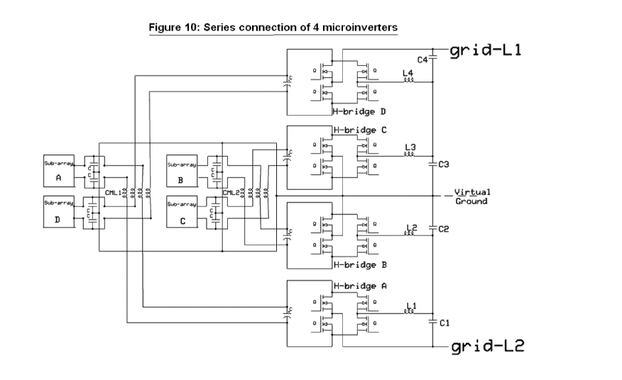
Figure 10 shows the series connection of four microinverters to a 240 V split-
phase grid.
Each inverter produces 60 volts RMS AC, for which the associated DC supply
voltages from Sub-
Arrays A, B, C and D must be at least 85 volts The two outer inverters labeled
H-bridge A and H-
bridge D are connected as in figure 9, namely with the output of the slowest
switching pair of
transistors connected to Li or L2. The common mode waveforms on sub-arrays A
and D are thus
85 volt peak to peak square waves with a 120 volt RMS sine wave subtracted
therefrom. These
waveforms are shown in figure 11, from which it may be seen that the common
mode waveforms
on sub-arrays A and D are merely antiphase versions of the same waveforms. A
joint common-
mode choke CM Ll may thus be used for sub-arrays A and D to connect to their
respective H-
bridges. Due to the waveforms being in antiphase, sub-array A connects to two
wires at the
opposite end of the winding of CM L1 compared to sub-array D. Figure 10 omits
details of the
connections of common-mode filter capacitors and damping components for
clarity, as its purpose
is only to show the use of joint common-mode chokes CML1 and CML2.
The inner two inverters comprising H-bridges B and C powered respectively by
DC from
sub-arrays B and C are substantially identical to figure 8 except for
operating with half the DC
voltage input and half the AC voltage output. The common mode waveforms are
thus 85 volt
peak-to-peak square waves as at nodes 111 and 112 of figure 8, scaled down by
a factor of 2:1.
Inverters B and C may thus also use a joint common mode choke CM L2.
9
CA 02989406 2017-12-13
WO 2016/204830 PCT/US2016/020406
The circuit of figure 10 may also be re-arranged so that the inner two
inverters are as per
figure 9 instead of as per figure 8, thus producing the common mode waveforms
of figure 9. If the
output pins of all four inverters are swapped, the circuit of figure 12 is
produced. Since the inner
two inverters H-bridges B and C are now connected as in figure 9, the common
mode waveforms
on their respective sub-arrays B and C are as per figure 9, namely an 85 volt
peak to peak square
wave from which is subtracted an 85-volt peak sine wave.
The common mode waveforms for the outer inverters A and D are the result of
adding an
85 volt peak sine wave to an 85 volt peak to peak square wave, resulting in
the waveforms 112
and 113 of figure 5, but of half the amplitude. Due to the reduced amplitude,
the concern for power
dissipation in the damping resistors is eliminated.
Inverters A and D of figure 12 may also use a joint common mode choke CML1 to
connect
to their respective sub-arrays A and D. Figure 12 shows the filter capacitors
of the common mode
filter (the 0.01 uF capacitors of figure 6) being returned to utility grid
neutral, as this is expected to
be the cleanest available line. The damping resistors may be returned to
different points however,
to reduce dissipation. For example, the damping resistors for inverters B and
C can be returned to
the 0-volt mean point, while the damping resistors for inverter A may be
returned to the junction of
Cl and C2, while the damping resistor for inverter D is returned to the
junction of 03 and C4.
Since the common mode waveforms in the case of four microinverters are of
reduced amplitude,
and thus the concern for damping resistor dissipation is reduced, the damping
resistors may be
returned to a consistent place for all four microinverters, namely to the
junction of 01 and C2 for
inverters A and B and to the junction of C3 and C4 for inverters C and D. This
allows the
construction of identical modules for all four microinverters.
As mentioned previously, when two microinverters such as A and B are joined at
the
junction of C1 and 02, the residual unfiltered ripple that passes through
their respective filters Ll,
Cl and L2, 02 should ideally be in phase at least for its dominant spectral
component. Thus no
ripple current at that frequency is created. When now the two inverter pairs,
each with their
dominant ripple component canceled, are joined at the junction of L2 and L3,
the second most
dominant ripple component from each inverter pair should be in-phase at that
point before they
are joined, thus avoiding creating ripple current also at the second most
dominant ripple spectral
component. This can be approximately arranged by using a common switching
controller to
coordinate the switching of all H-bridges to minimize total ripple currents or
voltages exported to
the grid that are not at the desired line frequency. In fact, using N
inverters in series (or parallel)
theoretically allows N-1 unwanted ripple components to be canceled.
Ripple cancellation of parallel- or series-connected microinverters may be
achieved by the
following consideration: When the clock frequency phase of a switching
inverter is shifted by Phi,
Fourier components at N times the clock frequency are shifted by N.Phi. Thus a
number M of
inverters connected in series or parallel and having their clock phase
relatively shifted by 0, Phi,
2Phi, 3Phi, (M-1)Phi will have ripple frequency components at N times the
clock frequency
CA 02989406 2017-12-13
WO 2016/204830
PCT/US2016/020406
shifted by 0, NPhi, 2NPhi, 3NPhi, (M-
1)NPhi. If Phi is chosen to be 27./M, the sum of such
ripple components is substantially canceled for N = 1, 2, ...., (M-1), thus
canceling the first M-1
harmonics of the switching frequency.
Microinverters may also be combined in parallel, as has been pioneered by
Enphase Inc.
However, according to the current invention, physically combining
microinverters in groups of two,
four or more can produce not only cost reductions due to sharing components
such as common
mode chokes, switching controllers and mechanical housings, but also produce
technical benefits
such as ripple reduction through using the common controller to coordinate
switching to that end.
In the case of paralleling microinverters, output currents and ripple currents
add; therefore
it is desired that the dominant components of the ripple currents cancel as
far as possible even
though the 60 Hz current components shall add in phase. This is again
facilitated by coordinating
the switching by means of a common controller.
Figure 13 shows four microinverters (200-A, 200-B, 200-C, 200-D) broadly
conforming to
the basic scheme of figure 1, connected in parallel to feed power to a 240
volt split-phase grid
connection though 2-pole GFI breaker (500). Each microinverter now has to
produce the full 240
volts RMS, which requires a DC input from their respective photovoltaic sub-
arrays (300-A, 300-B,
300-C, 300-D) of at least 340 volts. By co-housing the microinverters, they
can share common
components and in particular the octofilar common mode choke (400).
All of the microinverters of figure 13 operate in phase at 60 Hz, and so
create identical
common-mode waveforms. As there is no connection to ground or anything else
(apart from
capacitance of the solar arrays to ground), Kirchofts law requires that the
sum of the currents in
the L1, N and L2 paths through 2-pole GFI breaker (500) is zero; this is
exactly the condition for
not tripping the breaker. On the other hand, if an accidental path from any
array terminal to ground
were created, the current imbalance in GFI breaker (500) would cause it to
trip, interrupting the
ground fault leakage current. Moreover, disconnection of a grid-tie inverter
from the grid will cause
it to stop inverting, thus open the above mentioned output relays and
eliminating any AC or DC
voltages on the array relative to ground.
Any or all of microinverters 200-A to 200-D of figure 13 may be any of the
inverters
depicted in figures 3, 4, 8, 9, 10, or 12. For example, if inverters 200A-200D
each comprise a pair
of series connected inverters as in figure 4, the eight inverters may jointly
use a 16-filar common-
mode choke. Moreover, using a common switching controller for all eight
inverters allows seven
ripple components to be canceled by coordinating their switching.
In the prior art, microinverters were integrated with respective solar panels,
thereby
achieving the benefit of eliminating DC wiring, but hindering the use of
common components and
thus increasing cost. The inventive microinverter arrangements described above
may achieve
minimum system cost when all coupled microinverters are co-housed to allow use
of common
components. DC wiring is nevertheless still substantially eliminated if the co-
housed
microinverters are located sufficiently close to the array such that no DC
wiring is more than 10
11
CA 02989406 2017-12-13
WO 2016/204830 PCT/US2016/020406
feet away from the array. The 10 foot distance is defined in the National
Electrical Code as the
distance, beyond which the above mentioned new, unusual and onerous safety
requirements for
DC wiring apply, and which it is desired to avoid. A person skilled in the art
may devise many
configurations of coupled microinverters using the teachings disclosed herein,
all of which are
considered to fall within the scope and spirit of the invention as described
by the attached claims.
12