Note: Descriptions are shown in the official language in which they were submitted.
CA 02989409 2017-12-13
WO 2016/205249 PCT/US2016/037443
VIRTUAL AND AUGMENTED REALITY SYSTEMS AND METHODS
Priority Claim
[0001] This application claims the benefit of priority under 35 USC
119(e) of
U.S. Provisional Application No. 62/175994 filed on June 15, 2015 and of U.S.
Provisional
Application No. 62/180551 filed on June 16, 2015. Each of the above-identified
applications
is incorporated by reference herein in its entirety.
Incorporation by Reference
[0002] This application incorporates by reference in its entirety each
of the
following U.S. Patents and Patent Applications: U. S. Patent No. 6,334,960,
issued on
January 1, 2002, titled "Step and Flash Imprint Technology;" U.S. Patent No.
6,873,087,
issued on March 29, 2005, titled "High-Precision Orientation, Alignment and
Gap control
Stages for Imprint Lithography Processes;" U.S. Patent No. 6,900, 881, issued
on May 31,
2005, titled "Step and Repeat Imprint Lithography;" U.S. Patent No. 7,070,405,
issued on
July 4, 2006, titled "Alignment Systems for Imprint Lithography;" U.S. Patent
No. 7,122,482,
issued on October 17, 2006, titled "Methods for Fabricating Patterned Features
Utilizing
Imprint Lithography;" U.S. Patent No. 7,140,861, issued on November 28, 2006,
titled
"Compliant Hard Template for UV Imprinting;" U.S. Patent No. 8,076,386, issued
on
December 13, 2011, titled "Materials for Imprint Lithography;" U.S. Patent No.
7,098,572,
issued on August 29, 2006, titled "Apparatus to Control Displacement of a Body
Spaced
Apart from a Surface;" U.S. Application No. 14/641,376 filed on March 7, 2015;
U.S.
Application No. 14/555,585 filed on November 27, 2014; U.S. Application No.
14/690,401
filed on April 18, 2015; U.S. Application No. 14/212,961 filed on March 14,
2014; and U.S.
Application No. 14/331,218 filed on July 14,2014.
1
CA 02989409 2017-12-13
WO 2016/205249 PCT/US2016/037443
BACKGROUND
Field
[0003] The present disclosure relates to virtual reality and augmented
reality
imaging and visualization systems.
Description of the Related Art
[0004] Modern computing and display technologies have facilitated the
development of systems for so called "virtual reality" or "augmented reality"
experiences,
wherein digitally reproduced images or portions thereof are presented to a
user in a manner
wherein they seem to be, or may be perceived as, real. A virtual reality, or
"VR", scenario
typically involves presentation of digital or virtual image information
without transparency to
other actual real-world visual input; an augmented reality, or "AR", scenario
typically
involves presentation of digital or virtual image information as an
augmentation to
visualization of the actual world around the user. For example, referring to
Figure 1, an
augmented reality scene (1) is depicted wherein a user of an AR technology
sees a real-world
park-like setting (6) featuring people, trees, buildings in the background,
and a concrete
platform (1120). In addition to these items, the user of the AR technology
also perceives that
he "sees" a robot statue (1110) standing upon the real-world platform (1120),
and a cartoon-
like avatar character (2) flying by which seems to be a personification of a
bumble bee, even
though these elements (2, 1110) do not exist in the real world. Because the
human visual
perception system is complex, it is challenging to produce a VR or AR
technology that
facilitates a comfortable, natural-feeling, rich presentation of virtual image
elements amongst
other virtual or real-world imagery elements.
[0005] Systems and methods disclosed herein address various challenges
related
to VR and AR technology.
SUMMARY
[0006] The systems, methods and devices of the disclosure each have
several
innovative aspects, no single one of which is solely responsible for the
desirable attributes
disclosed herein.
2
CA 02989409 2017-12-13
WO 2016/205249 PCT/US2016/037443
[0007] In some embodiments, a display system is provided. The display
system
includes a waveguide; and an image injection device configured to direct a
multiplexed light
stream into the waveguide. The multiplexed light stream includes a plurality
of light streams
having different light properties. The waveguide includes in-coupling optical
elements
configured to selectively in-couple a first of the streams of light while
being transmissive to
one or more other streams of light. In some embodiments, the waveguide is part
of a stack of
waveguides, which can include a second waveguide including in-coupling optical
elements
configured to selectively turn a second of the streams of light while being
transmissive to one
or more other streams of light. In some embodiments, the in-coupling optical
elements of the
waveguide are configured to transmit at least one of the streams of light to
the in-coupling
optical elements of the second waveguide.
[0008] Various methods of manufacturing liquid crystal devices including
jet
depositing liquid crystal material on a substrate and using an imprint pattern
to align the
molecules of the liquid crystal are described herein. Using the methods
described herein,
devices including one or several layers of liquid crystal material can be
manufactured. Liquid
crystal devices manufactured using the methods described herein can include
liquid crystal
gratings including features and/or patterns that have a size less than about a
few microns.
Liquid crystal devices manufactured using the methods described herein can
also include
liquid crystal features and/or patterns that have a size less than the
wavelength of visible light
and may comprise what are referred to as Pancharatnam-Berry Phase Effect
(PBPE)
structures, metasurfaces, or metamaterials. In some cases, the small patterned
features in
these structures can be about 10 nm to about 100 nm wide and about 100 nm to
about 1
micron high. In some cases, the small patterned features in these structures
can be about 10
nm to about 1 micron wide and about 10 nm to about 1 micron high. Structures
for
manipulating light, such as for beam steering, wavefront shaping, separating
wavelengths
and/or polarizations, and combining different wavelengths and/or polarizations
can include
liquid crystal gratings with metasurface, otherwise referred to herein as
metamaterials liquid
crystal gratings or liquid crystal gratings with Pancharatnam-Berry Phase
Effect (PBPE)
structures. Liquid crystal gratings with PBPE structures can combine the high
diffraction
efficiency and low sensitivity to angle of incidence of liquid crystal
gratings with the high
3
CA 02989409 2017-12-13
WO 2016/205249 PCT/US2016/037443
wavelength sensitivity of the PBPE structures. Using the various methods of
manufacturing
described herein, liquid crystal gratings with PBPE structures can be mass-
produced which
may not be possible using the existing methods of disposing PBPE structures on
liquid
crystal materials. The methods discussed herein can also be used to fabricate
polarizers that
are more transparent than existing polarizers.
[0009] An innovative aspect of the subject material described herein is
included
in a method of manufacturing a liquid crystal device. The method comprises
depositing a
layer of liquid crystal material on a substrate; and imprinting a pattern on
the layer of liquid
crystal material using an imprint template, such that molecules of the liquid
crystal material
are self-aligned to the pattern.
[0010] Various embodiments of the method can include depositing a layer
of
material having a refractive index lower than refractive index of the liquid
crystal material.
The layer of low refractive index material can be configured as a
planarization layer using a
planarization template. In various embodiments, the imprint template can
include at least one
of surface relief features, features having a size between about 20 nm and
about 1 micron,
features having a size between about 10 nm and about 200 nm, PBPE structures,
a
metasurface, a grating array, curvilinear grooves or curvilinear arcs. Various
embodiments of
the method the layer of liquid crystal material can be deposited by jet
depositing the layer of
liquid crystal material. Various embodiments of the method can comprise
depositing an
additional layer of liquid crystal material over the layer of liquid crystal
material. The
additional layer of liquid crystal material can be self-aligned to the pattern
of the layer of
liquid crystal material. In various embodiments of the method a pattern can be
imprinted on
the additional layer of liquid crystal material. The pattern imprinted on the
additional layer of
liquid crystal material can be different from the pattern imprinted on the
layer of liquid
crystal material. The pattern imprinted on the layer of liquid crystal
material can be
configured to act on a first wavelength, and the pattern imprinted on the
additional layer of
liquid crystal material can be configured to act on a second wavelength.
[0011] Another innovative aspect of the subject material described
herein is
included in a method of manufacturing a liquid crystal device, the method
comprising:
depositing a layer of resist on a substrate; imprinting a pattern on the
resist layer using an
4
CA 02989409 2017-12-13
=
WO 2016/205249 PCT/US2016/037443
imprint template; and depositing a layer of liquid crystal material on the
patterned resist layer
such that molecules of the liquid crystal material are self-aligned to the
pattern.
[0012] In various embodiments of the method depositing a layer
of resist can
include jet depositing the resist layer. In various embodiments, the imprint
template can
include at least one of surface relief features, features having a size
between about 20 nm and
about 1 micron, PBPE structures, features having a size between about 10 nm
and about 200
nm, a metasurface, a grating array, curvilinear grooves or curvilinear arcs.
Various
embodiments of the method the layer of liquid crystal material can be
deposited by jet
depositing the layer of liquid crystal material. In various embodiments of the
method,
depositing a layer of liquid crystal material can include jet depositing the
layer of liquid
crystal material. Various embodiments of the method can further include
depositing an
additional layer of liquid crystal material over the layer of liquid crystal
material. The
additional layer of liquid crystal material can be self-aligned to the pattern
of the layer of
liquid crystal material. A pattern can be imprinted on the additional layer of
liquid crystal
material. The pattern imprinted on the additional layer of liquid crystal
material can be
different from the pattern imprinted on the layer of liquid crystal material.
The pattern
imprinted on the layer of liquid crystal material can be configured to act on
a first
wavelength, and the pattern imprinted on the additional layer of liquid
crystal material is
configured to act on a second wavelength.
[0013] Yet another innovative aspect of the subject matter
disclosed herein
includes a method of manufacturing a polarizer, the method comprising:
depositing a layer of
an optically transmissive material comprising a polymer on a substrate;
imprinting a pattern
on the polymer layer using an imprint template; and depositing a solution of
polarizer
material on the patterned polymer layer.
[0014] In various embodiments, depositing a solution of
polarizer material on the
patterned polymer layer can include jet depositing the polarizer material
solution on the
patterned polymer layer. In various embodiments, depositing a solution of
polarizer material
on the patterned polymer layer can include spin coating the polarizer material
solution on the
patterned polymer layer. In various embodiments, the polarizer material can
comprise a
CA 02989409 2017-12-13
=
WO 2016/205249 PCT/US2016/037443
solution of Iodine and dichroic dye in a solvent. The polarizer can have a
transmissivity of at
least 47%.
[00151 Yet another innovative aspect of the subject matter
disclosed herein
includes a liquid crystal device comprising a layer of liquid crystal
polarization gratings
comprising PBPE structures. The liquid crystal device can further comprise
another layer of
liquid crystal polarization gratings comprising PBPE structures. The liquid
crystal device can
be configured to selectively in-couple at least one light stream from a
multiplexed light
stream into the waveguide and transmit one or more other light streams from
the multiplexed
light stream. The liquid crystal device can be included in a waveguide of a
display system.
The liquid crystal device and/or the waveguide can be included in an eyepiece
of a head
mounted display.
[0016] Another innovative aspect of the subject matter
disclosed herein includes a
method of manufacturing an optical device including PBPE structures. The
method
comprises disposing a layer of a material that can transmit and/or reflect
incident light on a
substrate and imprinting a pattern including PBPE structures on the material.
The material
can comprise a liquid crystal. In various embodiments of the method, disposing
the material
can include jet depositing the material on the substrate. In various
embodiments of the
method, imprinting a pattern can comprise imprinting a pattern on the material
using an
imprint template including PBPE structures. The pattern imprinted on the
material can be
configured to selectively act on one or more wavelengths of light.
[0017] Yet another innovative aspect of the subject matter
disclosed herein
includes a method of manufacturing an optical device including a metasurface,
the method
comprises disposing a layer of a material that can transmit and/or reflect
incident light on a
substrate and imprinting a pattern including a metasurface on the material.
The material can
comprise a liquid crystal. The material can be jet deposited on the substrate.
In various
embodiments, imprinting a pattern can comprise imprinting a pattern on the
material using an
imprint template including a metasurface. In various embodiments, the pattern
imprinted on
the material can be configured to selectively act on one or more wavelengths
of light.
6
CA 02989409 2017-12-13
=
WO 2016/205249 PCT/US2016/037443
[0018] Another innovative aspect of the subject matter disclosed
herein includes a
method of manufacturing a liquid crystal device. The method comprises
depositing a layer
on a substrate; imprinting a pattern on the layer using an imprint template;
and depositing a
layer of liquid crystal material on the patterned layer such that molecules of
the liquid crystal
material are self-aligned to the pattern. The layer can comprise a resist
layer. In various
embodiments, depositing a layer can include jet depositing the layer. In some
embodiments,
the imprint template can include at least one of surface relief features,
features having a size
between about 10 nm and about 200 nm, features having a size between about 20
nm and
about 1 micron, PBPE structures, a metasurface, a grating array, curvilinear
grooves or arcs.
[0019] In various embodiments, depositing a layer of liquid crystal
material can
include jet depositing the layer of liquid crystal material. In various
embodiments, the
method can further include depositing an additional layer of liquid crystal
material over the
layer of liquid crystal material. The additional layer of liquid crystal
material can be self-
aligned to the pattern of the layer of liquid crystal material. A pattern can
be imprinted on the
additional layer of liquid crystal material. The pattern imprinted on the
additional layer of
liquid crystal material can be different from the pattern imprinted on the
layer of liquid
crystal material. The pattern imprinted on the layer of liquid crystal
material can be
configured to act on a first wavelength, and the pattern imprinted on the
additional layer of
liquid crystal material is configured to act on a second wavelength.
[0020] Another innovative aspect of the subject matter disclosed
herein includes a
method of manufacturing a polarizer, the method comprising depositing a layer
of an
optically transmissive material on a substrate; imprinting a pattern on the
material using an
imprint template; and depositing a solution of polarizer material on the
patterned polymer
layer.
[0021] Yet another innovative aspect of the subject matter disclosed
herein
includes a liquid crystal device. The liquid crystal device comprises a
substrate; a layer of
liquid crystal material have a first surface adjacent the substrate and a
second surface
opposite the first surface; and a plurality of features on the second surface,
the plurality of
features having a size between about 10 nm and about 200 nm. In various
embodiments, the
plurality of features can comprise at least one of PBPE structures, a meta-
surface, or a
7
CA 02989409 2017-12-13
WO 2016/205249 PCT/US2016/037443
metamaterial. In various embodiments, the plurality of features can be
configured as a
polarization grating. Embodiments of the liquid crystal device can be included
with a
waveguide of a display system. The liquid crystal device can be configured to
selectively in-
couple at least one light stream from a multiplexed light stream into the
waveguide and
transmit one or more other light streams from the multiplexed light stream.
The liquid crystal
device can be included in an eyepiece of a head mounted display.
[0022] Another innovative aspect of the subject matter disclosed herein
includes a
liquid crystal device comprising a substrate; a material have a first surface
adjacent the
substrate and a second surface opposite the first surface, the material
comprising a plurality
of features on the second surface having a size between about 10 nm and about
200 nm; and a
liquid crystal material on the second surface of the material. In various
embodiments, the
material can comprise a resist. In various embodiments, the plurality of
features can
comprise a meta-surface and/or a metamaterial. Embodiments of the liquid
crystal device can
be included with a waveguide of a display system. The liquid crystal device
can be
configured to selectively in-couple at least one light stream from a
multiplexed light stream
into the waveguide and transmit one or more other light streams from the
multiplexed light
stream. The liquid crystal device can be included in an eyepiece of a head
mounted display.
[0023] Details of' one or more embodiments of the subject matter
described in this
specification are set forth in the accompanying drawings and the description
below. Other
features, aspects, and advantages will become apparent from the description,
the drawings,
and the claims. Note that the relative dimensions of the following figures may
not be drawn
to scale.
BRIEF DESCRIPTION OF THE DRAWINGS
[0023] Figure 1 illustrates a user's view of augmented reality (AR)
through an AR
device.
[0024] Figure 2 illustrates an example of wearable display system.
[0025] Figure 3 illustrates a conventional display system for simulating
three-
dimensional imagery for a user.
[0026] Figure 4 illustrates aspects of an approach for simulating three-
dimensional imagery using multiple depth planes.
8
CA 02989409 2017-12-13
A
WO 2016/205249 PCT/US2016/037443
[0027] Figures
5A-5C illustrate relationships between radius of curvature and
focal radius.
[0028] Figure 6
illustrates an example of a waveguide stack for outputting image
information to a user.
[0029] Figure 7 shows an example of exit beams outputted by a
waveguide.
[0030] Figure
8A schematically illustrates a perspective view of an example of
the delivery of multiplexed image information into one or more waveguides.
[0031] Figure
8B schematically illustrates a perspective view of another example
of the delivery of multiplexed image information into multiple waveguides.
[0032] Figure
8C schematically illustrates a top-down view of the display system
of Figure 8B.
[0033] Figure
8D illustrates the display system of Figure 8C, with light
redirecting elements to out-couple light from each waveguide.
[0034] Figure
8E illustrates the display system of Figure 8B including an image
injection device comprising a light modulation device for providing x-y pixel
information.
[0035] Figure
9A illustrates an embodiment of a method of fabricating a liquid
crystal device.
[0036] Figures
9B and 9C illustrate embodiments of imprint templates that can be
used to fabricate liquid crystal devices in accordance with the method
described in Figure 9A
above or Figure 9D below.
[0037] Figure
9D illustrates another embodiment of a method of fabricating a
liquid crystal device.
[0038] Figure 9E, Figure 9F,
Figure 9G and Figure 9H illustrate various
embodiments of liquid crystal devices that can be manufactured using the
methods described
in Figures 9A or 9D.
[0039] Figure 91 illustrates
an embodiment of a resist layer imprinted with a
pattern as described in the method described in Figure 9D.
[0040] Figure 9J illustrates a
first imprint structure having discrete droplets or
sections that are oriented along a first direction and a second imprint
structure having discrete
9
CA 02989409 2017-12-13
WO 2016/205249 PCT/US2016/037443
droplets or sections that are oriented along a second direction that can be
combined to
produce optical devices with complex grating patterns.
[0041] Figure 9K and Figure 9L illustrate different polarizer
configurations that
can be fabricated using the jet deposition and imprinting methods described
herein.
[0042] Figure 9M illustrates an embodiment of a waveguide plate having a
light
entrance surface and a light exit surface that can change the polarization
state of incident
light.
[0043] Like reference numbers and designations in the various drawings
indicate
like elements.
DETAILED DESCRIPTION
[0044] Embodiments disclosed herein include optical systems, including
display
systems, generally. In some embodiments, the display systems are wearable,
which may
advantageously provide a more immersive VR or AR experience. For example,
displays
containing a stack of waveguides may be configured to be worn positioned in
front of the
eyes of a user, or viewer. In some embodiments, two stacks of waveguides, one
for each eye
of a viewer, may be utilized to provide different images to each eye.
[0045] Figure 2 illustrates an example of wearable display system (80).
The
display system (80) includes a display (62), and various mechanical and
electronic modules
and systems to support the functioning of that display (62). The display (62)
may be coupled
to a frame (64), which is wearable by a display system user or viewer (60) and
which is
configured to position the display (62) in front of the eyes of the user (60).
In some
embodiments, a speaker (66) is coupled to the frame (64) and positioned
adjacent the ear
canal of the user (in some embodiments, another speaker, not shown, is
positioned adjacent
the other ear canal of the user to provide for stereo/shapeable sound
control). The display
(62) is operatively coupled (68), such as by a wired lead or wireless
connectivity, to a local
data processing module (70) which may be mounted in a variety of
configurations, such as
fixedly attached to the frame (64), fixedly attached to a helmet or hat worn
by the user,
CA 02989409 2017-12-13
WO 2016/205249 PCT/US2016/037443
embedded in headphones, or otherwise removably attached to the user (60)
(e.g., in a
backpack-style configuration, in a belt-coupling style configuration).
[0046] The local processing and data module (70) may comprise a
processor, as
well as digital memory, such as non-volatile memory (e.g., flash memory), both
of which
may be utilized to assist in the processing, caching, and storage of data. The
data include
data a) captured from sensors (which may be, e.g., operatively coupled to the
frame (64) or
otherwise attached to the user (60)), such as image capture devices (such as
cameras),
microphones, inertial measurement units, accelerometers, compasses, GPS units,
radio
devices, and/or gyros; and/or b) acquired and/or processed using remote
processing module
(72) and/or remote data repository (74), possibly for passage to the display
(62) after such
processing or retrieval. The local processing and data module (70) may be
operatively
coupled by communication links (76, 78), such as via a wired or wireless
communication
links, to the remote processing module (72) and remote data repository (74)
such that these
remote modules (72, 74) are operatively coupled to each other and available as
resources to
the local processing and data module (70).
[0047] In some embodiments, the remote processing module (72) may
comprise
one or more processors configured to analyze and process data and/or image
information. In
some embodiments, the remote data repository (74) may comprise a digital data
storage
facility, which may be available through the intemet or other networking
configuration in a
"cloud" resource configuration. In some embodiments, all data is stored and
all computations
are performed in the local processing and data module, allowing fully
autonomous use from a
remote module.
[0048] The perception of an image as being "three-dimensional" or "3-D"
may be
achieved by providing slightly different presentations of the image to each
eye of the viewer.
Figure 3 illustrates a conventional display system for simulating three-
dimensional imagery
for a user. Two distinct images 74 and 76, one for each eye 4 and 6, are
outputted to the user.
The images 74 and 76 are spaced from the eyes 4 and 6 by a distance 10 along
an optical or z-
axis parallel to the line of sight of the viewer. The images 74 and 76 are
flat and the eyes 4
and 6 may focus on the images by assuming a single accommodated state. Such
systems rely
11
CA 02989409 2017-12-13
WO 2016/205249 PCT/US2016/037443
on the human visual system to combine the images 74 and 76 to provide a
perception of
depth for the combined image.
[0049] It will be appreciated, however, that the human visual system is
more
complicated and providing a realistic perception of depth is more challenging.
For example,
many viewers of conventional "3-D" display systems find such systems to be
uncomfortable
or may not perceive a sense of depth at all. Without being limited by theory,
it is believed
that viewers of an object may perceive the object as being "three-dimensional"
due to a
combination of vergence and accommodation. Vergence movements (i.e., rolling
movements
of the pupils toward or away from each other to converge the lines of sight of
the eyes to
fixate upon an object) of the two eyes relative to each other are closely
associated with
focusing (or "accommodation") of the lenses of the eyes. Under normal
conditions, changing
the focus of the lenses of the eyes, or accommodating the eyes, to change
focus from one
object to another object at a different distance will automatically cause a
matching change in
vergence to the same distance, under a relationship known as the
"accommodation-vergence
reflex." Likewise, a change in vergence will trigger a matching change in
accommodation,
under normal conditions. As noted herein, many stereoscopic or "3-D" display
systems
display a scene using slightly different presentations (and, so, slightly
different images) to
each eye such that a three-dimensional perspective is perceived by the human
visual system.
Such systems are uncomfortable for many viewers, however, since they, among
other things,
simply provide different presentations of a scene, but with the eyes viewing
all the image
information at a single accommodated state, and work against the
"accommodation-vergence
reflex." Display systems that provide a better match between accommodation and
vergence
may form more realistic and comfortable simulations of three-dimensional
imagery.
[0050] Figure 4 illustrates aspects of an approach for simulating three-
dimensional imagery using multiple depth planes. With reference to Figure 4A,
objects at
various distances from eyes 4 and 6 on the z-axis are accommodated by the eyes
(4, 6) so that
those objects are in focus. The eyes 4 and 6 assume particular accommodated
states to bring
into focus objects at different distances along the z-axis. Consequently, a
particular
accommodated state may be said to be associated with a particular one of depth
planes (14),
such that objects or parts of objects in a particular depth plane are in focus
when the eye is in
12
CA 02989409 2017-12-13
WO 2016/205249 PCT/US2016/037443
the accommodated state for that depth plane. In some embodiments, three-
dimensional
imagery may be simulated by providing different presentations of an image for
each of the
eyes (4, 6), and also by providing different presentations of the image
corresponding to each
of the depth planes.
[0051] The distance between an object and the eye (4 or 6) can change
the amount
of divergence of light from that object, as viewed by that eye. Figs. 5A-5C
illustrates
relationships between distance and the divergence of light rays. The distance
between the
object and the eye (4) is represented by, in order of decreasing distance, RI,
R2, and R3. As
shown in Figs. 5A-5C, the light rays become more divergent as distance to the
object
decreases. As distance increases, the light rays become more collimated.
Stated another
way, it may be said that the light field produced by a point (the object or a
part of the object)
has a spherical wavefront curvature, which is a function of how far away the
point is from the
eye of the user. The curvature increases with decreasing distance between the
object and the
eye (4). Consequently, at different depth planes, the degree of divergence of
light rays is also
different, with the degree of divergence increasing with decreasing distance
between depth
planes and the viewer's eye 4. While only a single eye (4) is illustrated for
clarity of
illustration in Figures 5A-5C and other figures herein, it will be appreciated
that the
discussions regarding eye (4) may be applied to both eyes (4 and 6) of a
viewer.
[0052] Without being limited by theory, it is believed that the human
eye typically
can interpret a finite of depth planes to provide depth perception.
Consequently, a highly
believable simulation of perceived depth may be achieved by providing, to the
eye, different
presentations of an image corresponding to each of these limited number of
depth planes.
[0053] Figure 6 illustrates an example of a waveguide stack for
outputting image
information to a user. A display system 1000 includes a stack of waveguides,
or stacked
waveguide assembly, (178) that may be utilized to provide three-dimensional
perception to
the eye/brain using a plurality of waveguides (182, 184, 186, 188, 190). In
some
embodiments, the display system (1000) is the system (80) of Figure 2, with
Figure 6
schematically showing some parts of that system (80) in greater detail. For
example, the
waveguide assembly (178) may be integrated into the display (62) of Figure 2.
13
CA 02989409 2017-12-13
WO 2016/205249 PCT/US2016/037443
[0054] With
continued reference to Figure 6, the waveguide assembly (178) may
also include a plurality of features (198, 196, 194, 192) between the
waveguides. In some
embodiments, the features (198, 196, 194, 192) may be lens. The waveguides
(182, 184, 186,
188, 190) and/or the plurality of lenses (198, 196, 194, 192) may be
configured to send image
information to the eye with various levels of wavefront curvature or light ray
divergence.
Each waveguide level may be associated with a particular depth plane and may
be configured
to output image information corresponding to that depth plane. Image injection
devices (200,
202, 204, 206, 208) may be utilized to inject image information into the
waveguides (182,
184, 186, 188, 190), each of which may be configured, as described herein, to
distribute
incoming light across each respective waveguide, for output toward the eye 4.
Light exits an
output surface (300, 302, 304, 306, 308) of the image injection devices (200,
202, 204, 206,
208) and is injected into a corresponding input edge (382, 384, 386, 388, 390)
of the
waveguides (182, 184, 186, 188, 190). In some embodiments, a single beam of
light (e.g. a
collimated beam) may be injected into each waveguide to output an entire field
of cloned
collimated beams that are directed toward the eye (4) at particular angles
(and amounts of
divergence) corresponding to the depth plane associated with a particular
waveguide.
[0055] In some
embodiments, the image injection devices (200, 202, 204, 206,
208) are discrete displays that each produce image information for injection
into a
corresponding waveguide (182, 184, 186, 188, 190, respectively). In some
other
embodiments, the image injection devices (200, 202, 204, 206, 208) are the
output ends of a
single multiplexed display which may, e.g., pipe image information via one or
more optical
conduits (such as fiber optic cables) to each of the image injection devices
(200, 202, 204,
206,208).
[0056] A controller
210 controls the operation of the stacked waveguide assembly
(178) and the image injection devices (200, 202, 204, 206, 208). In some
embodiments, the
controller 210 includes programming (e.g., instructions in a non-transitory
medium) that
regulates the timing and provision of image information to the waveguide (182,
184, 186,
188, 190) according to, e.g., any of the various schemes disclosed herein. In
some
embodiments, the controller may be a single integral device, or a distributed
system
14
CA 02989409 2017-12-13
WO 2016/205249 PCT/US2016/037443
connected by wired or wireless communication channels. The controller 210 may
be part of
the processing modules (70 or 72) (Figure 2) in some embodiments.
[0057] The waveguides (182, 184, 186, 188, 190) may be configured to
propagate
light within each respective waveguide by total internal reflection (TIR). The
waveguides
(182, 184, 186, 188, 190) may each be planar, with major top and bottom
surfaces and edges
extending between those major top and bottom surfaces. In the illustrated
configuration, the
waveguides (182, 184, 186, 188, 190) may each include light redirecting
elements (282, 284,
286, 288, 290) that are configured to redirect light, propagating within each
respective
waveguide, out of the waveguide to output image information to the eye 4. A
beam of light is
outputted by the waveguide at locations at which the light propagating in the
waveguide
strikes a light redirecting element. The light redirecting elements (282, 284,
286, 288, 290)
may be reflective and/or diffractive optical features. While illustrated
disposed at the bottom
major surfaces of the waveguides (182, 184, 186, 188, 190) for ease of
description and
drawing clarity, in some embodiments, the light redirecting elements (282,
284, 286, 288,
290) may be disposed at the top and/or bottom major surfaces, and/or may be
disposed
directly in the volume of the waveguides (182, 184, 186, 188, 190). In some
embodiments,
the light redirecting elements (282, 284, 286, 288, 290) may be formed in a
layer of material
that is attached to a transparent substrate to form the waveguides (182, 184,
186, 188, 190).
In some other embodiments, the waveguides (182, 184, 186, 188, 190) may be a
monolithic
piece of material and the light redirecting elements (282, 284, 286, 288, 290)
may be formed
on a surface and/or in the interior of that piece of material.
[0058] With continued reference to Figure 6, as discussed herein, each
waveguide
(182, 184, 186, 188, 190) is configured to output light to form an image
corresponding to a
particular depth plane. For example, the waveguide (182) nearest the eye may
be configured
to deliver collimated light, as injected into such waveguide (182), to the eye
(4). The
collimated light may be representative of the optical infinity focal plane.
The next waveguide
up (184) may be configured to send out collimated light which passes through
the first lens
(192; e.g., a negative lens) before it can reach the eye (4); such first lens
(192) may be
configured to create a slight convex wavefront curvature so that the eye/brain
interprets light
coming from that next waveguide up (184) as coming from a first focal plane
closer inward
CA 02989409 2017-12-13
WO 2016/205249 PCT/US2016/037443
toward the eye (4) from optical infinity. Similarly, the third up waveguide
(186) passes its
output light through both the first (192) and second (194) lenses before
reaching the eye (4);
the combined optical power of the first (192) and second (194) lenses may be
configured to
create another incremental amount of wavefront curvature so that the eye/brain
interprets
light coming from the third waveguide (186) as coming from a second focal
plane that is
even closer inward toward the person from optical infinity than was light from
the next
waveguide up (184).
[0059] The other waveguide layers (188, 190) and lenses (196, 198) are
similarly
configured, with the highest waveguide (190) in the stack sending its output
through all of the
lenses between it and the eye for an aggregate focal power representative of
the closest focal
plane to the person. To compensate for the stack of lenses (198, 196, 194,
192) when
viewing/interpreting light coming from the world (144) on the other side of
the stacked
waveguide assembly (178), a compensating lens layer (180) may be disposed at
the top of the
stack to compensate for the aggregate power of the lens stack (198, 196, 194,
192) below.
Such a configuration provides as many perceived focal planes as there are
available
waveguide/lens pairings. Both the light redirecting elements of the waveguides
and the
focusing aspects of the lenses may be static (i.e., not dynamic or electro-
active). In some
alternative embodiments, they may be dynamic using electro-active features.
[0060] With continued reference to Figure 6, the light redirecting
elements (282,
284, 286, 288, 290) may be configured to both redirect light out of their
respective
waveguides and to output this light with the appropriate amount of divergence
or collimation
for a particular depth plane associated with the waveguide. As a result,
waveguides having
different associated depth planes may have different configurations of light
redirecting
elements (282, 284, 286, 288, 290), which output light with a different amount
of divergence
depending on the associated depth plane. In some embodiments, as discussed
herein, the
light redirecting elements (282, 284, 286, 288, 290) may be volumetric or
surface features,
which may be configured to output light at specific angles. For example, the
light redirecting
elements (282, 284, 286, 288, 290) may be volume holograms, surface holograms,
and/or
diffraction gratings. Light redirecting elements, such as diffraction
gratings, are described in
U.S. Patent Application No. 14/641,376, filed March 7, 2015, which is
incorporated by
16
CA 02989409 2017-12-13
WO 2016/205249 PCMS2016/037443
reference herein in its entirety. In some embodiments, the features (198, 196,
194, 192) may
not be lenses; rather, they may simply be spacers (e.g., cladding layers
and/or structures for
forming air gaps).
[0061] In some embodiments, the light redirecting elements (282, 284,
286, 288,
290) are diffractive features that form a diffraction pattern, or "diffractive
optical element"
(also referred to herein as a "DOE"). Preferably, the DOE's have a relatively
low diffraction
efficiency so that only a portion of the light of the beam is deflected away
toward the eye (4)
with each intersection of the DOE, while the rest continues to move through a
waveguide via
total internal reflection. The light carrying the image information is thus
divided into a
number of related exit beams that exit the waveguide at a multiplicity of
locations and the
result is a fairly uniform pattern of exit emission toward the eye (4) for
this particular
collimated beam bouncing around within a waveguide.
[0062] In some embodiments, one or more DOEs may be switchable between
"on" states in which they actively diffract, and "off" states in which they do
not significantly
diffract. For instance, a switchable DOE may comprise a layer of polymer
dispersed liquid
crystal, in which microdroplets comprise a diffraction pattern in a host
medium, and the
refractive index of the microdroplets can be switched to substantially match
the refractive
index of the host material (in which case the pattern does not appreciably
diffract incident
light) or the microdroplet can be switched to an index that does not match
that of the host
medium (in which case the pattern actively diffracts incident light).
[0063] Figure 7 shows an example of exit beams outputted by a waveguide.
One
waveguide is illustrated, but it will be appreciated that other waveguides in
the stack of
waveguides (178) may function similarly. Light (400) is injected into the
waveguide (182) at
the input edge (382) of the waveguide (182) and propagates within the
waveguide (182) by
TIR. At points where the light (400) impinges on the DOE (282), a portion of
the light exits
the waveguide as exit beams (402). The exit beams (402) are illustrated as
substantially
parallel but, as discussed herein, they may also be redirected to propagate to
the eye (4) at an
angle (e.g., forming divergent exit beans), depending on the depth plane
associated with the
waveguide (182). It will be appreciated that substantially parallel exit beams
may be
indicative of a waveguide that corresponds to a depth plane at a large
distance (e.g., optical
17
CA 02989409 2017-12-13
WO 2016/205249 PCT/US2016/037443
infinity) from the eye (4). Other waveguides may output an exit beam pattern
that is more
divergent, which would require the eye (4) to accommodate to a closer distance
to bring it
into focus on the retina and would be interpreted by the brain as light from a
distance closer
to the eye (4) than optical infinity.
PART I. MULTIPLEXED IMAGE INFORMATION
[0064] With reference again to Figure 6, utilizing a dedicated image
injection
device (200, 202, 204, 206, or 208) for each waveguide (182, 184, 186, 188, or
190) may be
mechanically complex and may require a large volume to accommodate all of the
image
injection devices and their related connections. A smaller form factor may be
desirable for
some applications, such as wearable displays.
[0065] In some embodiments, a smaller form factor may be achieved by
using a
single image injection device to inject information into a plurality of the
waveguides. The
image injection device delivers multiple image information streams (also
referred to herein as
information streams) to the waveguides, and these information streams may be
considered to
be multiplexed. Each waveguide includes in-coupling optical elements that
interact with the
information streams to selectively in-couple image information from a
particular information
stream into that waveguide. In some embodiments, the in-coupling optical
elements
selectively redirect light from a particular information stream into its
associated waveguide,
while allowing light for other information streams to continue to propagate to
other
waveguides. The redirected light is redirected at angles such that it
propagates through its
associated waveguide by TIR. Thus, in some embodiments, a single image
injection device
provides a multiplexed information stream to a plurality of waveguides, and
each waveguide
of that plurality of waveguides has an associated information stream that it
selectively in-
couples using in-coupling optical elements.
[0066] The selective interaction between the in-coupling optical
elements and the
information streams may be facilitated by utilizing information streams with
different optical
properties. For example, each information stream may be formed by light of
different colors
(different wavelengths) and/or different polarizations (preferably different
circular
polarizations). In turn, the in-coupling optical elements are configured to
selectively redirect
18
CA 02989409 2017-12-13
WO 2016/205249 PCT/US2016/037443
light of a particular polarization and/or of one or more particular
wavelengths, thereby
allowing a specific correspondence, e.g., one-to-one correspondence, between
an information
stream and a waveguide. In some embodiments, the in-coupling optical elements
are
diffractive optical elements configured to selectively redirect light based
upon the properties
of that light, e.g., the wavelength and/or polarization of that light.
[0067] In some embodiments, each image injection device provides image
information to a plurality of two, three, four, or more waveguides by
providing, respectively,
two, three, four, or more information streams to that plurality of waveguides.
In some
embodiments, multiple such image injection devices may be used to provide
information to
each of multiple pluralities of waveguides.
[0068] With reference now to Figure 8A, an example of the delivery of
multiplexed image information into one or more waveguides is illustrated
schematically in a
perspective view. A stack 3000 includes waveguides 3002 and 3004, which
include in-
coupling optical elements 3012 and 3014, respectively. In some embodiments,
the
waveguides 3002 and 3004 may be substantially planar plates, each having a
front and rear
major surface and edges extending between these front and rear major surfaces.
For example,
waveguide 3002 has front major surface 3002a and rear major surface 3002b. The
major
surfaces of the waveguides may include a cladding layer (not illustrated) to
facilitate the TIR
of light within each waveguide. In some embodiments, the stack 3000 of
waveguides
corresponds to the stack 178 of Figure 6 and may be utilized to replace the
stack 178 in the
display systems disclosed herein.
[0069] With continued reference to Figure 8A, light streams A and B have
different light properties, e.g., different wavelengths and/or different
polarizations (preferably
different circular polarizations). The light streams A and B include distinct
image
information streams. Light A and B and their information streams are
propagated through
optical conduit 3024 (e.g., an optical fiber) as a multiplexed information
stream to an image
injection device 3021. The image injection device injects light 3040
(containing the
multiplexed information stream as combined light streams A and B) into the
waveguide stack
3000.
19
CA 02989409 2017-12-13
WO 2016/205249 PCT/US2016/037443
[0070] In some embodiments, the image injection device 3021 includes an
actuator 3020 (such as a piezoelectric actuator) that is coupled to an optical
fiber 352, which
may be used to scan the fiber tip of the fiber 352 across an area of the stack
3000. Examples
of such scanning fiber image injection devices are disclosed in U.S. Patent
Application No.
14/641,376, filed March 7,2015, which is incorporated by reference herein in
its entirety. In
some other embodiments, the image injection device 3021 may be stationary and,
in some
embodiments, may direct light towards the stack 3000 from multiple angles.
[0071] In some embodiments, each waveguide includes in-coupling optical
elements. For example, waveguide 3002 includes in-coupling optical elements
3012, and
waveguide 3004 includes in-coupling optical elements 3014. The in-coupling
optical
elements 3012 and 3014 are configured to selectively redirect one of light
streams A and B.
For example, in-coupling optical elements 3012 may selectively redirect at
least a portion of
light stream A to in-couple that light stream into the light guide 3002. The
in-coupled
portion of light stream A propagates through the waveguide 3002 as light 3042.
In some
embodiments, the light 3042 propagates through the waveguide 3002 by TIR off
the major
surfaces 3002a and 3002b of that waveguide. Similarly, in-coupling optical
elements 3014
may selectively redirect at least a portion of light stream B to in-couple
that light stream into
the light guide 3004. The in-coupled portion of light stream B propagates
through the
waveguide 3004 as light 3044. In some embodiments, the light 3044 propagates
through the
waveguide 3004 by TIR off the major surfaces 3004a and 3004b of that
waveguide.
[0072] As illustrated, in some embodiments, the multiplexed light stream
3040
includes both light streams A and B simultaneously, and light stream A may be
in-coupled to
waveguide 3002 while light stream B is in-coupled to waveguide 3004, as
discuss above. In
some other embodiments, light streams A and B may be provided to the waveguide
stack
3000 at different times. In such embodiments, only a single waveguide may be
utilized to
receive these information streams, as discussed herein. In either case, the
light streams A and
B may be coupled to the optical conduit 3024 by the optical coupler 3050. In
some
embodiments, the optical coupler 3050 may combine light streams A and B for
propagation
through the optical conduit 3024.
CA 02989409 2017-12-13
WO 2016/205249 PCT/US2016/037443
[0073] With continued reference to Figure 8A, in some embodiments,
optics 3030
may be disposed between the image injection device 3021 and the in-coupling
optical
elements 3012 and 3014. The optics 3030 may include, e.g., lens that
facilitating directing
light rays onto the various in-coupling optical elements 3012 and 3014, e.g.,
by focusing the
light onto in-coupling optical elements 3012 and 3014. In some embodiments,
the optics are
part of the image injection device 3021 and may be, e.g., a lens at the end of
the image
injection device 3021. In some embodiments, optics 3030 may be omitted
completely.
[0074] It will be appreciated that the in-coupling optical elements 3012
and 3014
are configured to selectively redirect the light streams A and B based upon
one or more light
properties that differ between those light streams. For example, light stream
A may have a
different wavelength than light stream B and the in-coupling optical elements
3012 and 3014
may be configured to selectively redirect light based on wavelength.
Preferably, the different
wavelengths correspond to different colors, which can improve the selectivity
of the in-
coupling optical elements relative to using different wavelengths of the same
color.
[0075] In some embodiments, light stream A may have a different
polarization
than light stream B and the in-coupling optical elements 3012 and 3014 may be
configured to
selectively redirect light based on polarization. For example, the in-coupling
optical
elements 3012 and 3014 may be configured to selectively redirect light based
on polarization.
In some embodiments, the light streams A and B have different circular
polarization. In
some embodiments, the light streams A and B may have multiple differences in
light
properties, including, e.g., both different wavelengths and different
polarizations.
[0076] In some embodiments, in-coupling optical elements 3012 and 3014
are
diffractive optical elements, including diffractive gratings (e.g., a grating
comprising liquid
crystal such as a liquid crystal polarization grating). In some embodiments,
the optical
element may include a meta-surface (e.g., comprise a PBPE), such as a surface
have a pattern
with feature sizes on the order of one's or ten's of nanometers. Examples of
suitable in-
coupling optical elements 3012 and 3014 include the optical elements 2000b,
2000d (Figure
9A) and the optical elements of Figures 9E-9H. Advantageously, such optical
elements are
highly efficient at selectively redirecting light of different polarizations
and/or different
wavelengths.
21
CA 02989409 2017-12-13
a
WO 2016/205249 PCT/US2016/037443
[0077] With
reference now to Figure 8B, another example of the delivery of
multiplexed image information into multiple waveguides is illustrated
schematically in a
perspective view. It will be appreciated that the stack 3000 can include more
than two
waveguides, e.g., 4, 6, 8, 10, 12, or other numbers of waveguides, so long as
image
information can be adequately provided to individual waveguides and to a
user's eyes
through the stack 3000. The illustrated stack 3000 includes waveguides 3006
and 3008 in
addition to the waveguides 3002 and 3004. The waveguides 3006 and 3008 include
in-
coupling optical elements 3012 and 3014, respectively. In some embodiments,
the
waveguides 3002, 3004, 3006, and 3008 may be similar, except for the in-
coupling optical
elements, which may each be configured to redirect and in-couple light having
different light
properties. In some
other embodiments, in-coupling optical elements for multiple
waveguides may be similar. It will be appreciated that all the disclosure
herein related to
Figure 8A apply to Figure 8B, except that the number of waveguides in Figure
8B is greater
than in Figure 8A.
[0078] With
continued reference to Figure 8B, light streams A, B, C, and D have
different light properties, e.g., different wavelengths and/or different
polarizations (preferably
different circular polarizations). For example, light streams A, B, C, and D
may each include
light of different wavelengths. In some other embodiments, various
combinations of
different wavelengths and polarizations are possible. For example, A and B may
have similar
wavelengths and different polarizations, and C and D may have similar
wavelengths and
different polarizations, with A and B different from C and D. Light streams A,
B, C, and D
are propagated through optical conduit 3024 as a multiplexed information
stream to the
image injection device 3021, which injects light 3040 of the multiplexed
information stream
into the waveguide stack 3000. As discussed herein, the multiplexed
information stream may
include all light streams simultaneously, or one or more of the light streams
may be directed
to the stack 3000 at different times.
[0079] In some
embodiments, each waveguide includes in-coupling optical
elements that selectively in-couple light into that waveguide. For example,
waveguide 3002
includes in-coupling optical elements 3012, which may be configured to in-
couple light
stream A into that waveguide, so that it propagates by T1R in that waveguide
as light 3042;
22
CA 02989409 2017-12-13
WO 2016/205249 PCMS2016/037443
waveguide 3004 includes in-coupling optical elements 3014, which may be
configured to in-
couple light stream B into that waveguide, so that it propagates by TR in that
waveguide as
light 3044; waveguide 3006 includes in-coupling optical elements 3016, which
may be
configured to in-couple light stream C into that waveguide, so that it
propagates by TIR in
that waveguide as light 3046; and waveguide 3008 includes in-coupling optical
elements
3018, which may be configured to in-couple light stream D into that waveguide,
so that it
propagates by UR in that waveguide as light 3048.
[0080] It will be appreciated that, in some embodiments, a single light
stream
(e.g., light stream A, B, C, or D) may be in-coupled to a single waveguide. In
some other
embodiments, multiple light streams may be in-coupled to the same waveguide.
Preferably,
in such an arrangement, the light streams are in-coupled at different times.
In some
embodiments, such temporally separated in-coupling may be achieved using in-
coupling
optical elements that selectively turn light based on multiple different light
properties (e.g.,
multiple different wavelengths or multiple different polarizations), while the
image injection
device provides the information streams for a particular waveguide at
different times. For
example, both light streams A and B may be in-coupled to waveguide 3002, with
the in-
coupling optical elements 3012 selectively in-coupling light streams A and B
while allowing
light streams C and D to pass through, and with the light streams A and B
providing light to
the in-coupling optical elements 3012 at different times while simultaneously
providing light
streams C and/or D to the in-coupling optical elements 3012. It will be
appreciated that one
or more other waveguides may be similarly configured to in-couple multiple
light streams to
those waveguides.
[0081] In some other embodiments, multiple light streams (e.g., light
streams A
and B) may be provided simultaneously to the in-coupling optical elements
(e.g., in-coupling
optical elements 3012), and the in-coupling optical elements may be configured
to change
states to choose between in-coupling light stream A or B. For example, in some
embodiments, the in-coupling optical elements may be a grating formed of
liquid crystal
material disposed between electrodes (e.g., transparent electrodes such as
ITO). The liquid
crystal may change states (e.g., orientations) with the application of a
voltage potential, with
one state configured to selectively in-couple one light stream (e.g., light
stream A) and
23
CA 02989409 2017-12-13
WO 2016/205249 PCT/US2016/037443
another state configured to be transparent to all light streams (e.g., both
light stream A and
B). In some embodiments, another layer of switchable liquid crystal material,
forming a
different grating, may be provided between electrodes, with one state
configured to
selectively in-couple a different light stream (e.g., light stream B) and
another state
configured to be transparent to all light streams (e.g., both light stream A
and B). In some
other embodiments, both types of liquid crystal material may be disposed on
the same level,
but in different areas. The liquid crystal material may be configured such
that when one type
of material is transparent to the light streams, the other type selectively in-
couples light of a
particular light stream, and vice versa.
[0082] Now with reference to Figure 8C, a top-down schematic view of the
display system of Figure 8B is illustrated. The top-down view is taken looking
down along a
top edge of the stack 3000 of Figure 8B. As illustrated, in some embodiments,
portions of
multiplexed light stream 3040 are selectively in-coupled into each of
waveguides 3002, 3004,
3006, and 3008 as in-coupled light 3042, 3044, 3046, and 3048.
[0083] As discussed herein, the waveguides may include light redirecting
elements (e.g., light redirecting elements (282, 284, 286, 288, 290)) that
output or out-couple
light, which has been propagating inside the waveguide, so that the out-
coupled light
propagates towards the eyes 4 of a viewer (Figure 6). Figure 8D illustrates
the display system
of Figure 8C, with light redirecting elements to out-couple light from each
waveguide. For
example, waveguide 3002 includes out-coupling light redirecting elements 3062,
waveguide
3004 includes out-coupling light redirecting elements 3064, waveguide 3006
includes out-
coupling light redirecting elements 3066, and waveguide 3008 includes out-
coupling light
redirecting elements 3068. In some embodiments, the out-coupling light
redirecting elements
may include different groups of light redirecting elements, each of which
functions
differently. For example, out-coupling light redirecting elements 3062 may
include a first
group of light redirecting elements 3062a and a second group of light
redirecting elements
3062b. For example, light redirecting elements 3062b may be exit pupil
expanders (EPEs; to
increase the dimensions of the eye box in at least one axis), and light
redirecting elements
3062a may be orthogonal pupil expanders (OPEs; to increase the eye box in an
axis crossing,
e.g., orthogonal to, the axis of the EPEs). EPEs and OPEs are disclosed in
U.S. Provisional
24
CA 02989409 2017-12-13
WO 2016/205249 PCT/US2016/037443
Patent Application No. 62/005,807, filed May 30, 2014, the entire disclosure
of which is
incorporated by reference herein.
[0084] It will be appreciated that images are formed by the waveguides
using
information streams with encoded x-y pixel information. For example, the
information
streams of different colors may each indicate the intensity of light for a
particular location on
an x-y grid corresponding to the x-y pixel information for the image. Without
being limited
by theory, it will also be appreciated that the matching of information
streams to waveguides
is achieved using the properties of light and is not necessarily dependent
upon the x-y pixel
information provided by that light. Consequently, the x-y pixel information
may be encoded
at any suitable location using any suitable device along the path of the light
before the light
impinges on the in-coupling optical elements 3012, 3014, 3016, and 3018.
[0085] In some embodiments, if a light source (e.g., LED or OLED) is
pixilated
and is able to output light having the desired light properties (e.g., desired
wavelengths and/or
polarizations), then an information stream may be formed having both the
desired light
properties and encoded x-y pixel information as it is emitted from the light
source. In some
other embodiments, light having the desired light properties is passed through
a light
modulation device in which the x-y pixel information is encoded. Figure 8E
illustrates the
display system of Figure 8B and shows a light modulation device 3070 for
providing x-y
pixel information to the image information stream. In some embodiments, the
light
modulation device 3070 may be part of the image injection device 3021, and may
be
configured to provide image information using a scanning fiber, or one or more
stationary
aperture display devices for providing image information to the waveguides. In
some
embodiments, the light modulation device 3070 modifies the light as it passes
through the
device (e.g., the intensity of the light may be modified by being passed
through pixel
elements having controllable variable light transmission). In some other
embodiments, the
light modulation device may modify light by selectively redirecting (e.g.,
reflecting) light to
propagate into the waveguide stack 3000. Examples of light modulation devices
include
transmissive liquid crystal displays and micro-mirror devices (such as a
"digital light
processing", or "DLP" system, such as those available from Texas Instruments,
Inc.).
CA 02989409 2017-12-13
WO 2016/205249 PCT/US2016/037443
PART II. LIQUID CRYSTAL POLARIZATION GRATINGS WITH
PANCHARATNAM-BERRY PHASE EFFECT (PBPE) STRUCTURES
10086] This section
relates to liquid crystals, polarization gratings, and
Pancharatnam-Berry Phase Effect (PBPE) structures, methods of fabrication
thereof as well
as other structures and methods. In some embodiments, methods and apparatus
are provided
for manufacturing liquid crystal grating structures that have high diffraction
efficiency, low
sensitivity to angle of incident and high wavelength sensitivity. Various
methods described
herein include disposing a layer of liquid crystal material using inkjet
technology and using
an imprint template to align the liquid crystal material.
[0087] In some
embodiments, the liquid crystals, polarization gratings, and
Pancharatnam-Berry Phase Effect (PBPE) structures disclosed in this Part II
may be utilized
to form light redirecting elements for the various waveguides of the waveguide
stacks 178
(Figure 6) or 3000 (Figures 8A-8E). For example, such liquid crystals,
polarization gratings,
and Pancharatnam-Berry Phase Effect (PBPE) structures may advantageously be
applied to
form the various in-coupling optical elements disclosed herein, including the
in-coupling
optical elements 3012, 3014, 3016, and/or 3018 (Figure 8A-8E).
[0088] A variety of
imaging systems and optical signal processing systems can
include liquid crystal devices to control/manipulate an optical wavefront,
wavelength,
polarization, phase, intensity, angle and/or other properties of light. Liquid
crystals are partly
ordered materials whose molecules are often shaped like rods or plates or some
other forms
that can be aligned along a certain direction. The direction along which the
molecules of the
liquid crystal are oriented can be manipulated by application of
electromagnetic forces which
can be used to control/manipulate the properties of light incident on the
liquid crystal
material.
[0089] Methods of
manufacturing liquid crystal devices and certain resulting
structures are described herein.
[0090] The
following detailed description is directed to certain embodiments for
the purposes of describing the innovative aspects. However, the teachings
herein can be
applied in a multitude of different ways. As will be apparent from the
following description,
26
CA 02989409 2017-12-13
WO 2016/205249 PCT/US2016/037443
the innovative aspects may be implemented in any optical component or device
that is
configured to manipulate one or more characteristics of incident light.
[0091] As discussed more fully below, innovative aspects described
herein
include fabricating liquid crystal devices using jet deposition technology.
For example, in an
embodiment of a method of manufacturing a liquid crystal device, a layer of
liquid crystal
material is deposited on a substrate using jet deposition technology (e.g.,
inkjet technology).
Surface relief features (e.g., PBPE structures) can be imprinted in the layer
of the jet
deposited liquid crystal material using a template. The surface relief
features may be
configured (e.g., with particular spacing and/or heights) to achieve
particular light redirecting
properties. In some other embodiments, imprinting can be repeated on different
levels to
produce successive layered cross-sections that, in combination, can behave as
volumetric
features (such as exists in "bulk" volume-phase materials and devices. In
various
embodiments, these surface relief features (and the successive layered cross-
sections) can be
modeled as "Bragg" structures. Generally, such structures can be used to
produce binary
surface-relief features in which there exists a material-to-air interface,
resist-to-air interface,
resin-to-air interface or a liquid crystal material-to-air interface that
produces diffraction, or a
material-to-lower index resist interface, resist-to-lower index resist
interface, resin-to- lower
index resist interface or a liquid crystal material-to- lower index resist
interface that does the
same. In these cases the gratings can be modeled as "raman-nath" structures,
rather than
Bragg structures. The molecules of the liquid crystal material are aligned
through the process
of imprinting due to the physical shape of the nanostructures and their
electrostatic
interaction with the liquid crystal (LC) material. Alignment of the liquid
crystal layer using
the imprint pattern is discussed in greater detail below.
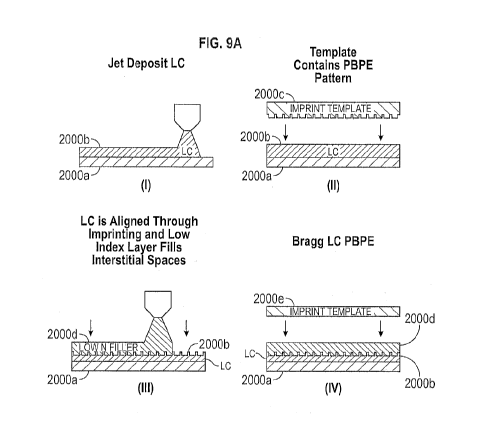
[0092] In various embodiments, a layer of material, (e.g., a polymer),
to serve as a
photo-alignment layer, may be deposited using jet deposition technology (in
which a jet or
stream of material is directed onto a substrate), e.g., via ink-jet onto a
substrate or pre-coated
substrate. The photo-alignment layer is patterned by nano-imprinting using a
template
incorporating the desired LC orientation pattern. In some embodiments, this
pattern is a
PBPE pattern, and the template, comprising a physical relief, may be made with
interferometric and/or lithographic techniques. The template is lowered on to
the soft
27
CA 02989409 2017-12-13
WO 2016/205249 PCT/US2016/037443
polymer resin and UV light is used to cure the resin to a fixed state. In some
embodiments,
capillary action fills the template with the polymer material before it is
cured. The template
is retracted, leaving the patterned, cured resin in place on the substrate. A
second step, using
a deposition process (e.g., jet or spin coating) applies a layer of LC (e.g.,
LC suspended in
resin) on top of the photo-alignment layer. The LC aligns to the photo-
alignment layer
pattern below it, and when this occurs, the resin is fixed in place using UV
light, heat, or a
combination of both. In some other embodiments, LC suspended in solvent (e.g.,
resin) is
deposited (e.g., dispensed using jet or spin coating), and the template
containing the
nanoimprint pattern (e.g., a PBPE pattern) is lowered into contact with the LC
material, to
the LC takes up the relief profile of the template (e.g., by capillary action
into the openings in
the template), and the LC material is fixed in place using a cure process
(e.g., UV, heat or a
combination of both). The resulting structure may be used directly as a
functional element,
or in some cases, a low refractive index material can be deposited over the
imprinted liquid
crystal material to fill the interstitial areas between the surface features
imprinted in the liquid
crystal material.
[0093] The low refractive index material can be configured as a
planarization
layer by tuning the viscoelastic and chemical properties of the liquid
crystals based resist or
by contacting the top surface of the low refractive index material with a
planarization imprint
template (e.g., a template having a substantially planar surface). In some
other embodiments,
the low refractive index material can be planarized by a chemical and/or
mechanical
planarization process. The planarization process is preferably chosen to form
a planarized
surface that is smooth, to reduce optical artifacts that may be caused by a
rough surface.
Additional layers such as additional liquid crystal layers can be deposited
using the jet
technology over the liquid crystal layer. The PBPE structures in the different
layers of liquid
crystal can be configured to diffract, steer, and/or disperse or combine
different wavelengths
of light. For example, red, green and blue wavelengths can be diffracted,
dispersed, or
redirected along different directions by the PBPE structures in the different
liquid crystal
layers.
[0094] The different liquid crystal layers are preferably formed with
materials that
provide sufficient structural stability and adhesion to allow layers to be
stacked over one
28
CA 02989409 2017-12-13
WO 2016/205249 PCT/US2016/037443
another. In some embodiments, organic or inorganic imprint resist materials,
including
polymerizable materials that form optically transmissive cured structures, may
be used. As
an example, the liquid crystal layers can include an acrylic liquid crystal
formulation. Acrylic
liquid crystal layers can provide adhesive properties that facilitate the
stacking of layers on
top of each other.
[0095] It will be appreciated that, as discussed herein both the liquid
crystal
material and the low refractive index material may be flowable materials. In
some
embodiments, these materials may be subjected to a process to immobilize them
after contact
with the imprint templates and before removing the contacting template. The
immobilization
process may include a'curing process, as discussed herein.
[0096] As another example, in another embodiment of a method of
manufacturing
a liquid crystal device, a layer of a photoresist material (e.g., a resin or a
polymer) is
deposited on a substrate. The deposition may be accomplished by various
deposition
methods, including spin coating. More preferably, in some embodiments, the
deposition is
accomplished using jet technology (e.g., inkjet technology). The photoresist
is imprinted
with an imprint template or mold having surface relief features (e.g., PBPE
structures). A
layer of liquid crystal material can be deposited using jet technology on the
imprinted layer of
photoresist. The imprinted photoresist layer can serve as an aligning layer to
align the
molecules of the liquid crystal material as it is deposited. Additional layers
such as
additional liquid crystal layers or layers not comprising liquid crystal can
be deposited using
the jet technology over the liquid crystal layer. In various embodiments, a
planarization layer
can be deposited over the deposited liquid crystal layer.
[0097] In embodiments discussed herein, different types of liquid
crystal
materials, such as, for example, doped liquid crystal, un-doped liquid
crystal, and other non-
liquid crystal materials can be deposited using inkjet technology. Inkjet
technology can
provide thin controlled (e.g., uniform) thickness of the deposited liquid
crystal layer or
planarization layer. Inkjet technology can also provide layers of different
thickness such as
layers of liquid crystal or other layers having a different thickness in
different areas on the
surface and can accommodate different pattern height and keep a constant
residual layer
thickness underneath the imprinted patterns. Inkjet technology is
advantageously capable of
29
CA 02989409 2017-12-13
WO 2016/205249 PCT/US2016/037443
providing thin layers, for example between about 10 nm and 1 micron; or
between about 10
nm and about 10 microns in thickness and can reduce waste in comparison with
other
techniques such as spin coating. The inkjet technology can facilitate
deposition of different
liquid crystal compositions on the same substrate. In addition, inkjet nano-
imprinting can
produce a very thin residual layer thickness. In the illustrated embodiments,
the uniform area
below the imprint pattern can correspond to the residual layer. PBPE and other
diffractive
structures can exhibit variable and sometimes enhanced performance with very
thin or zero
residual layer thickness. Inkjet nano-imprinting approaches can be used to
deposit different
types of materials across a given substrate simultaneously, and can be used to
produce
variable thickness materials in different areas of a single substrate
simultaneously. This may
be beneficial to PBPE structures, particularly when they are combined in a
single substrate
with more conventional diffractive structures which may require other
materials and/or
thicknesses of resist.
CA 02989409 2017-12-13
WO 2016/205249 PCT/US2016/037443
[0098] The liquid crystal layers deposited by jet technology can be
cured using
UV curing, thermal methods, freezing, annealing and other methods. The imprint
template
can include complex groove geometries (e.g., grooves with multiple steps,
gratings with
different orientations, etc.). Liquid crystal devices manufactured using the
methods described
herein can include liquid crystal layers comprising gratings with different
orientations and
different PBPE structures.
[0099] The manufacturing methods using inkjet technology described
herein can
also be configured to manufacture polarizers having increased transmissivity
and/or wave
plates comprising subwavelength features and/or metamaterials. These and other
aspects are
discussed in detail below.
[0100] Figure 9A illustrates an embodiment of a method of fabricating a
liquid
crystal device, preferably using inkjet technology. In the embodiment of the
method
illustrated in Figure 9A, a layer 2000b of liquid crystal material is
deposited on a substrate
2000a, e.g., using inkjet technology, as shown in panel (i). The liquid
crystal material can
include a doped or an un-doped liquid crystal material. In various
embodiments, the liquid
crystal material can be a polymer stabilized nematic liquid crystal material.
The substrate
2000a can include glass, plastic, sapphire, a polymer or any other substrate
material. The
layer 2000b of the liquid crystal material can have a thickness between about
20 nanometers
and 2 microns. In some embodiments, the layer 2000b of the liquid crystal
material can have
a thickness between about 0.5 microns and about 10 microns.
[0101] The layer 2000b of the liquid crystal material can be imprinted
with an
imprint pattern 2000c including wavelength and sub-wavelength scale surface
features, as
shown in panel (ii). The surface features can include PBPE structures that can
directly
manipulate the phase of the incoming light. Without any loss of generality, a
PBPE structure
can be thought of as a type of polarization grating structure. In various
embodiments, the
imprint pattern 2000c can include an array of grooves comprising PBPE
structures. The array
of grooves can form a liquid crystal grating structure that can have high
diffraction efficiency
and low sensitivity to incident angle. The grooves can have a depth between
about 20 nm
and about lmicron and a width between about 20 nm and about 1 micron. In some
embodiments, the grooves can have a depth between about 100 nm and about 500
nm and a
31
CA 02989409 2017-12-13
WO 2016/205249 PCT/U52016/037443
width between about 200 nm and about 5000 nm. In some embodiments, the grooves
can
have a depth between about 20 nm and about 500 nm and a width between about 10
nm and
about 10 micron. The PBPE structures can include sub-wavelength patterns that
encode
phase profile directly onto the local orientation of the optical axis. The
PBPE structures can
be disposed on the surface of the liquid crystal grating structures. The PBPE
structures can
have feature sizes between about 20 nm and about 1 micron. In some
embodiments, the
PBPE structures can have feature sizes between about 10 nm and about 200 nm.
In some
embodiments, the PBPE structures can have feature sizes between about 10 nm
and about
800 nm. In various embodiments, an underlying PBPE structure can be used as an
alignment
layer for volumetric orientation of LC. The volumetric component in this case
happens
automatically, as the LCs naturally align themselves to the alignment layer.
In another
embodiment, it may be desirable to differentially align multiple layers
containing PBPE
alignment and LC layers, to change diffraction properties of the system as a
composite ¨ for
example to multiplex multiple wavelength operation since each sub-layer would
act on only a
select subset of wavelengths.
[0102] In various embodiments, the imprint pattern 2000c can include a
simple
geometric pattern, such as, for example, a plurality of grooves or more
complicated pattern
such as multi-tier geometry including a plurality of grooves and recesses as
shown in figure
9B. In various embodiments, the imprint pattern 2000c can include a plurality
of imprint
layers, each imprint layer including a different imprint pattern as shown in
figure 9C. In the
imprint pattern shown in figure 9C, the imprint layers 2000c-1, 2000c-2 and
2000c-3 include
a plurality of grooves with progressively decreasing space between adjacent
grooves. In
various embodiments, the imprint pattern can include patterns such as chevron,
spirals, arcs,
etc. The imprint pattern can be fabricated on a semiconductor material or
other structure
using methods such as e-beam lithography or other lithography methods.
[0103] Referring to figure 9A, the layer 2000b of the liquid crystal
material is
aligned to the imprinted pattern. The spaces between adjacent grooves can be
filled with a
material 2000d. In some embodiments, filling material may comprise a
transparent material
having a lower refractive index less than the refractive index of the liquid
crystal material, as
shown in panel (iii). Such a configuration can be used, for example, in a
waveguide
32
CA 02989409 2017-12-13
WO 2016/205249 PCT/US2016/037443
structure. In this manner a high refractive index difference can be obtained
between the
liquid crystal grating structures and its surrounding such that the liquid
crystal gratings can
have high diffraction efficiency. As mentioned above, the PBPE LC grating may
be made
material-to-air interface, a resist-to-air interface, resin-to-air interface
or liquid crystal
material-to-air interface, where air is the low index "material". However, in
some cases it
may be desirable to place another layer of material on top of the prior
patterned layer,
possibly in intimate contact, and in this case it may be desirable to dispense
and planarize a
low-index curable resin that preserves the differential index of refraction
between PBPE
structures, but that also provide a laminate-able layer above. In various
embodiments, the
liquid crystal gratings can be configured as Bragg liquid crystal gratings. In
various
embodiments, the layer of low refractive index material 2000d can be
configured as a
planarization layer. In such embodiments, the layer of low refractive index
material 2000d
can be configured to be planarized by another imprint pattern 2000e, as shown
in panel (iv).
[0104] Figure 9D illustrates another embodiment of a method of
fabricating a
liquid crystal device, preferably using inkjet technology. In the embodiment
of the method
illustrated in Figure 9A, a layer 2000f of a resist is deposited on a
substrate 2000a using
inkjet technology, as shown in panel (i). The resist can include materials
such as, for
example, organic and inorganic based imprint materials, resins or polymers.
For example,
the resist can include materials disclosed in U.S. Patent No. 8,076,386 which
is incorporated
by reference herein in its entirety. In some embodiments, the resist layer 9F
can have a
thickness between about 20 nm and about 1 micron. In some embodiments, the
resist layer
9F can have a thickness between about 10 nm and about 5 micron. The resist
layer 2000f can
be imprinted with an imprint pattern 2000c including volume and/or surface
features, as
shown in panel (ii). A layer 2000b of liquid crystal material can be disposed
by inkjet on the
imprinted resist layer 2000f, as shown in panel (iii). The imprinted resist
layer can serve to
align the liquid crystal material as it is jet deposited onto the imprinted
resist layer 2000f.
[0105] The liquid crystal devices fabricated using above described
methods can
be cured using UV curing, thermal curing, freezing or other curing methods.
[0106] Another embodiment of a method to fabricate liquid crystal
devices
includes imprinting a desired alignment structure in UV curable resist using
Jet and FlashTm
33
CA 02989409 2017-12-13
WO 2016/205249 PCT/US2016/037443
Imprint Lithography (J-FIL); and dispensing a liquid crystal polymer
formulation from inkjet.
The liquid crystal polymer can have a high solvent content, for example, to
provide
sufficiently low viscosity to enable efficient egress through the inkjets.
In various
embodiments, the liquid crystal polymer can be in an isotropic state as it is
dispensed. In
some embodiments, the liquid crystal polymer can be configured to align along
the alignment
structure in the resist by driving off the solvent. Additional liquid crystal
polymer layers can
be disposed on top of the disposed liquid crystal polymer layer by following
the method
described above. The formulation and the viscosity of the liquid crystal
material in the
solvent may also be adjusted to achieve rapid drying process for the dispensed
liquid crystal
materials.
[0107] Figures 9E-
9H illustrate embodiments of liquid crystal gratings fabricated
using the methods described above. Figure 9E illustrates a single layer liquid
crystal grating
including PBPE structures that have high diffraction efficiency, high
wavelength sensitivity
and low sensitivity to incident angle. The liquid crystal gratings illustrated
in Figure 9E can
be manufactured using the process depicted in Figure 9A. For example, a liquid
crystal
polymer LCP I can be deposited on a substrate and an imprint template can be
used to imprint
a pattern on the liquid crystal polymer LCPl such that the molecules of the
liquid crystal
polymer LCP1 are self-aligned to the imprinted pattern. The pattern can
include a
metasurface (e.g., PBPE structures). Figure 9F illustrates a liquid crystal
grating including
PBPE structures that have high diffraction efficiency, high wavelength
sensitivity and low
sensitivity to incident angle. In the embodiment illustrated in Figure 9F, the
liquid crystal
gratings can be manufactured using the process depicted in Figure 9D. For
example, an
alignment layer comprising a polymer (e.g., a resist or a resin) can be
deposited on a substrate
and an imprint template can be used to imprint a pattern on the polymer. A
layer of liquid
crystal material is deposited on the alignment layer such that the molecules
of the liquid
crystal layer are aligned to the pattern imprinted on the alignment layer. The
pattern can be
part of a metasurface (e.g., PBPE structures). In various embodiments, PBPE
structure of the
first liquid crystal layer (LCP1) can serve as the alignment structure for the
second liquid
layer (LCP2).
[0108] Figure 9G
illustrates a three layer liquid crystal grating including PBPE
34
CA 02989409 2017-12-13
WO 2016/205249 PCT/US2016/037443
structures that have high diffraction efficiency, high wavelength sensitivity
and low
sensitivity to incident angle. The multi-layer liquid crystal gratings can be
manufactured
using the processes depicted in Figures 9A or 9D. For example, using the
process of Figure
9D, the multi-layer liquid crystal gratings illustrated in Figure 9G can be
manufactured by
aligning the molecules of a first liquid crystal layer (LCP1) using a first
alignment layer
comprising a first imprint pattern deposited on the substrate, aligning the
molecules of a
second liquid crystal layer (LCP2) using a second alignment layer comprising a
second
imprint pattern deposited on the first alignment layer and aligning the
molecules of a third
liquid crystal layer (LCP3) using a third alignment layer comprising a third
imprint pattern
deposited on the second alignment layer. In some embodiments, the process of
Figure 9A
may be utilized to form one or more of the first, second, and third liquid
crystal layers have
aligned liquid crystal molecules (LCP1, LCP2, and LCP3, respectively). In
such
embodiments, each of LCP1, LCP2, and LCP3 may be formed by imprinting a
pattern in a
liquid crystal layer deposited over the substrate. The imprinting may be
accomplished using
an imprint template having a pattern that causes the liquid crystal molecules
to align to the
pattern. The imprint template may subsequently be removed and a filler may be
deposited
into the gaps left by the imprint template removal.
[0109] With
continued reference to Figure 9G, the first, second and third imprint
patterns can each be a metasurface (e.g., PBPE structures). The first, second
and third
imprint patterns can be different such that each imprint pattern is configured
to selectively
diffract/redirect different wavelengths of light in an incident beam to couple
each of the
different wavelengths in one or more waveguides. In some embodiments, the
different
wavelengths of light in an incident beam can be coupled into the one or more
waveguides at
the same angle. However, in some other embodiments, as discussed below, the
different
wavelengths of light in an incident beam can be coupled into the one or more
waveguides at
different wavelengths. In some other embodiments, the PBPE structure of the
first liquid
crystal layer (LCP1) can serve as the alignment structure for the second
liquid layer (LCP2)
which in turn can serve as the alignment structure for the third liquid layer
(LCP3). The
embodiment illustrated in Figure 9G can include different PBPE structures such
that different
wavelengths of light in an incident beam of light are diffracted or redirected
at different
CA 02989409 2017-12-13
WO 2016/205249 PCT/US2016/037443
output angles such that they are spatially separated. In various embodiments,
the incident
beam of light can be monochromatic or polychromatic. Conversely, the multi-
layer liquid
crystal structure can be used to combine different wavelengths of light as
illustrated in Figure
9H.
[0110] Figure 91 illustrates a cross-section of a resist layer imprinted
with an
imprint pattern illustrated in figure 9B.
[0111] As discussed above, the liquid crystal layer can be formed with a
variety of
materials. For example, in some embodiments, an acrylate liquid crystal
formulation can be
disposed over the polymer align imprint structure using inkjet and imprint
technology.
Acrylate composition can facilitate stacking different liquid crystal layers
on top of each
other that can adhere to each other without adhesive layers thereby making
process simpler.
Different liquid crystal layers can be stacked to achieve a desired effect,
for example, the
desired polarization, diffraction, steering, or dispersion effect.
[0112] The method described above can be used to fabricate liquid
crystal
polarization gratings and patterned guiding layers using linear submasters
with jet dispensing
technology (e.g., J-FIL). Different liquid crystal grating structures can be
fabricated by
combining structure with different shapes, orientations, and/or pitches. This
process is
described in more detail with reference to Figure 9J which illustrates a first
imprint structure
having discrete droplets or sections that are oriented along a first direction
and a second
imprint structure having discrete droplets or sections that are oriented along
a second
direction. The discrete droplets or sections of the first and the second
imprint structures can
be dispersed using inkjet technology. The discrete droplets or sections of the
first and the
second imprint structures can merge or not merge in different embodiments. The
discrete
droplets or sections in the first and the second imprint structures can be
combined to produce
an imprint structure with discrete droplets or sections having different
orientations. Liquid
crystal material can be disposed on the combined imprint pattern to produce
liquid crystal
gratings with molecules aligned along different orientations. The different
orientations of the
separate sections together can produce a more complex grating pattern,
similar, for example,
to that of a PBPE, in the aggregate.
[0113] The inkjet and imprint methods discussed herein can be used to
fabricate
36
CA 02989409 2017-12-13
WO 2016/205249 PCT/US2016/037443
other optical elements such as waveguide plates, optical retarders,
polarizers, etc. For
example, a polarizer that is more transparent than existing polarizers can be
fabricated using
the methods described herein. The method includes disposing a transparent or
substantially
transparent material that is patterned such as a polymer imprint and
depositing a polarizer
material, such as, for example, an iodine solution containing dichroic dye.
The method
includes imprinting a pattern on the transparent polymer. The pattern can be
linear grooves,
chevrons, spirals, arcs, or any other simple or complicated pattern. For
example, the pattern
can be a periodic linear grating structure. The polarizer material can then be
deposited on the
patterned transparent polymer using the jet technology (such as, for example,
J-F1L)
described above, imprint planarization or by spin coating. Figure 9K and 9L
illustrate
different polarizer configurations that can be fabricated using the methods
described above.
The polarizers fabricated using the technology described herein can be more
transparent than
existing polarizers. Such a component may be useful for devices that utilize
low extinction
ratio polarizers such as a waveguide stack for head mounted display eyepieces
for augmented
and virtual reality as described elsewhere herein.
[0114] Subwavelength scale grating structures can induce birefringence
in
materials. For example, single dimensional grating can act as artificial
negative uniaxial
materials whose optical axes are parallel to the grating vector. Such
birefringence can be
referred to as form birefringence. Accordingly, substrates including
subwavelength scale
grating structures can function as wave plates. The amount of retardation
provided by
substrates including subwavelength scale grating structures can depend on the
dimension
(e.g., height, width, pitch, etc.) of the grating patterns as well as the
material refractive index.
For example, a material with higher index comprising a pattern of
subwavelength scale
features can provide higher retardation than a material with lower index
comprising a similar
pattern of subwavelength scale features. Inkjet and imprint technology, such
as, for example,
J-FIL allows high throughput Ultra Violet Nano-Imprint Lithography (UV-NIL)
patterning
capabilities with very low waste of material over any defined area. Inkjet and
imprint
technology, such as, for example, J-FIL can also facilitate repeated stacking
of imprinted
layers. Imprint layers (single or multi-layered) with such subwavelength scale
grating
structures with or without varying geometry / orientation can provide varying
degrees of
37
CA 02989409 2017-12-13
WO 2016/205249 PCT/US2016/037443
phase-shift. Embodiments of patterned birefringent materials can enhance thin
film
integration capabilities in various optical applications.
[0115] The
polarization of light output from substrates including subwavelength
scale grating structures can depend on the orientation, shape and/or pitch of
the
subwavelength scale grating structures. Embodiments
of wave plates including
subwavelength scale grating structures can also be fabricated using the inkjet
and imprint
methods described herein. Figure 9M illustrates an embodiment of a waveguide
plate 2005
having a light entrance surface 2006 and a light exit surface 2007. The
waveguide plate 2005
can include a plurality of subwavelength scale grating features with varying
shapes,
orientations and/or pitches such that incident unpolarized light is output as
a polarized light.
In various embodiments, the wave plate 2005 can include multiple stacks of
thin transparent
films 2009a, 2009b and 2009c that are imprinted with subwavelength scale
grating features
with varying shapes, orientations and/or pitches. The grating features can be
imprinted on the
transparent films using an imprint template as shown in Figure 9C. In various
embodiments,
the transparent films 2009a, 2009b and 2009c can comprise imprintable resists
having
refractive index between about 1.45 and 1.75. The polarization of the light
output from a
multilayer structure can depend on the shapes, orientations and/or pitches of
the grating
structures as well as refractive index difference between the different
layers. For the
embodiment illustrated in Figure 9M, incident unpolarized light is converted
to right
circularly polarized light by the waveguide plate 2005. In other embodiments,
the waveguide
plate can be configured to provide linearly polarized light, left circularly
polarized light or
light with any other polarization characteristic.
[0116] It is
contemplated that the innovative aspects may be implemented in or
associated with a variety of applications such as imaging systems and devices,
display
systems and devices, spatial light modulators, liquid crystal based devices,
polarizers, wave
guide plates, etc. The structures, devices and methods described herein may
particularly find
use in displays such as wearable displays (e.g., head mounted displays) that
can be used for
augmented and/or virtually reality. More generally, the described embodiments
may be
implemented in any device, apparatus, or system that can be configured to
display an image,
whether in motion (such as video) or stationary (such as still images), and
whether textual,
38
CA 02989409 2017-12-13
=
WO 2016/205249 PCT/US2016/037443
graphical or pictorial. It is contemplated, however, that the described
embodiments may be
included in or associated with a variety of electronic devices such as, but
not limited to:
mobile telephones, multimedia Internet enabled cellular telephones, mobile
television
receivers, wireless devices, smartphones, Bluetooth devices, personal data
assistants
(PDAs), wireless electronic mail receivers, hand-held or portable computers,
netbooks,
notebooks, smartbooks, tablets, printers, copiers, scanners, facsimile
devices, global
positioning system (GPS) receivers/navigators, cameras, digital media players
(such as MP3
players), camcorders, game consoles, wrist watches, clocks, calculators,
television monitors,
flat panel displays, electronic reading devices (e.g., e-readers), computer
monitors, auto
displays (including odometer and speedometer displays, etc.), cockpit controls
and/or
displays, camera view displays (such as the display of a rear view camera in a
vehicle),
electronic photographs, electronic billboards or signs, projectors,
architectural structures,
microwaves, refrigerators, stereo systems, cassette recorders or players, DVD
players, CD
players, VCRs, radios, portable memory chips, washers, dryers, washer/dryers,
parking
meters, head mounted displays and a variety of imaging systems. Thus, the
teachings are not
intended to be limited to the embodiments depicted solely in the Figures, but
instead have
wide applicability as will be readily apparent to one having ordinary skill in
the art.
[0117] Various modifications to the embodiments described in this
disclosure
may be readily apparent to those skilled in the art, and the generic
principles defined herein
may be applied to other embodiments without departing from the spirit or scope
of this
disclosure. Thus, the claims are not intended to be limited to the embodiments
shown herein,
but are to be accorded the widest scope consistent with this disclosure, the
principles and the
novel features disclosed herein. The word "exemplary" is used exclusively
herein to mean
"serving as an example, instance, or illustration." Any embodiment described
herein as
"exemplary" is not necessarily to be construed as preferred or advantageous
over other
embodiments. Additionally, a person having ordinary skill in the art will
readily appreciate,
the terms "upper" and "lower", "above" and "below", etc., are sometimes used
for ease of
describing the figures, and indicate relative positions corresponding to the
orientation of the
figure on a properly oriented page, and may not reflect the proper orientation
of the structures
described herein, as those structures are implemented.
39
= CA 02989409 2017-12-13
WO 2016/205249 PCT/US2016/037443
[0118] Certain features that are described in this specification in
the context of
separate embodiments also can be implemented in combination in a single
embodiment.
Conversely, various features that are described in the context of a single
embodiment also can
be implemented in multiple embodiments separately or in any suitable
subcombination.
Moreover, although features may be described above as acting in certain
combinations and
even initially claimed as such, one or more features from a claimed
combination can in some
cases be excised from the combination, and the claimed combination may be
directed to a
subcombination or variation of a subcombination.
[0119] Similarly, while operations are depicted in the drawings in
a particular
order, this should not be understood as requiring that such operations be
performed in the
particular order shown or in sequential order, or that all illustrated
operations be performed,
to achieve desirable results. Further, the drawings may schematically depict
one more
example processes in the form of a flow diagram. However, other operations
that are not
depicted can be incorporated in the example processes that are schematically
illustrated. For
example, one or more additional operations can be performed before, after,
simultaneously,
or between any of the illustrated operations. In certain circumstances,
multitasking and
parallel processing may be advantageous. Moreover, the separation of various
system
components in the embodiments described above should not be understood as
requiring such
separation in all embodiments, and it should be understood that the described
program
components and systems can generally be integrated together in a single
software product or
packaged into multiple software products. Additionally, other embodiments are
within the
scope of the following claims. In some cases, the actions recited in the
claims can be
performed in a different order and still achieve desirable results.
[0120] Various example embodiments of the invention are described
herein.
Reference is made to these examples in a non-limiting sense. They are provided
to illustrate
more broadly applicable aspects of the invention. Various changes may be made
to the
invention described and equivalents may be substituted without departing from
the true spirit
and scope of the invention. In addition, many modifications may be made to
adapt a
particular situation, material, composition of matter, process, process act(s)
or step(s) to the
objective(s), spirit or scope of the present invention. Further, as will be
appreciated by those
CA 02989409 2017-12-13
WO 2016/205249 PCT/US2016/037443
with skill in the art that each of the individual variations described and
illustrated herein has
discrete components and features which may be readily separated from or
combined with the
features of any of the other several embodiments without departing from the
scope or spirit of
the present inventions. All such modifications are intended to be within the
scope of claims
associated with this disclosure.
[0121] The invention includes methods that may be performed using the
subject
devices. The methods may comprise the act of providing such a suitable device.
Such
provision may be performed by the end user. In other words, the "providing"
act merely
requires the end user obtain, access, approach, position, set-up, activate,
power-up or
otherwise act to provide the requisite device in the subject method. Methods
recited herein
may be carried out in any order of the recited events which is logically
possible, as well as in
the recited order of events.
[0122] Example aspects of the invention, together with details regarding
material
selection and manufacture have been set forth above. As for other details of
the present
invention, these may be appreciated in connection with the above-referenced
patents and
publications as well as generally known or appreciated by those with skill in
the art. The
same may hold true with respect to method-based aspects of the invention in
terms of
additional acts as commonly or logically employed.
[0123] In addition, though the invention has been described in reference
to several
examples optionally incorporating various features, the invention is not to be
limited to that
which is described or indicated as contemplated with respect to each variation
of the
invention. Various changes may be made to the invention described and
equivalents (whether
recited herein or not included for the sake of some brevity) may be
substituted without
departing from the true spirit and scope of the invention. In addition, where
a range of values
is provided, it is understood that every intervening value, between the upper
and lower limit
of that range and any other stated or intervening value in that stated range,
is encompassed
within the invention.
[0124] Also, it is contemplated that any optional feature of the
inventive
variations described may be set forth and claimed independently, or in
combination with any
one or more of the features described herein. Reference to a singular item,
includes the
41
CA 02989409 2017-12-13
WO 2016/205249 PCT/US2016/037443
possibility that there are plural of the same items present. More
specifically, as used herein
and in claims associated hereto, the singular forms "a," "an," "said," and
"the" include plural
referents unless the specifically stated otherwise. In other words, use of the
articles allow for
"at least one" of the subject item in the description above as well as claims
associated with
this disclosure. It is further noted that such claims may be drafted to
exclude any optional
element. As such, this statement is intended to serve as antecedent basis for
use of such
exclusive terminology as "solely," "only" and the like in connection with the
recitation of
claim elements, or use of a "negative" limitation.
[0125] Without the use of such exclusive terminology, the term
"comprising" in
claims associated with this disclosure shall allow for the inclusion of any
additional element--
irrespective of whether a given number of elements are enumerated in such
claims, or the
addition of a feature could be regarded as transforming the nature of an
element set forth in
such claims. Except as specifically defined herein, all technical and
scientific terms used
herein are to be given as broad a commonly understood meaning as possible
while
maintaining claim validity.
[0126] The breadth of the present invention is not to be limited to the
examples
provided and/or the subject specification, but rather only by the scope of
claim language
associated with this disclosure.
42