Note: Descriptions are shown in the official language in which they were submitted.
TITLE OF INVENTION
GAP SENSOR AND GAP MEASURING METHOD
TECHNICAL FIELD
The present invention relates to a gap sensor for and
a gap measuring method of detecting a gap, in particular,
surface-distributed gaps between the surfaces of members
that face each other.
BACKGROUND ART
In technology of assembling ships, aircraft, and the
like, attaching an external panel to an internal part
requires an alignment of relative positions. For example, a
main wing of an aircraft has a box structure including beams
and ribs. A base end part of the main wing has a frame
structure to be joined with a fuselage. The fuselage has a
fixing part (bracket) substantially having a cylindrical
structure to receive the base end part of the main wing.
The base end part of the main wing is inserted into the
fixing part and joined to the same to form a tea-caddy-like
structure. The fixing part of the fuselage is constructed
to have two plate members that hold therebetween a plate
member constituting the base end part of the main wing. The
surface of the plate member of the base end part faces the
plate members of the fixing part with a gap of about several
millimeters between them. Each of the plate members is made
of conductive material such as aluminum alloy and carbon
fiber. In the joining work of the fuselage and main wing,
they are aligned and adjusted to each other to establish a
predetermined positional relationship. Thereafter, a spacer
adjusted to the shape of the gap is inserted into the gap
and is joined to the adjoining members. The same is carried
CA 2989869 2989869 2017-12-22
out when manufacturing a fuselage by separately preparing a
front fuselage, a middle fuselage, and a rear fuselage and
joining them together into one body. Related arts are, for
example, Japanese Patent Publication NO. 4832512 and
Japanese Unexamined Patent Application Publication No. 2015-
79979.
SUMMARY OF INVENTION
Problems to be Solved by Invention
After aligned to each other, the plate member of the
base end part of the main wing and the plate members of the
fixing part of the fuselage define gaps at joined positions.
The gaps are multipoint-measured with a gap sensor (a feeler
gauge, a thickness gauge) to obtain three-dimensional data
on the shape of a gap space to determine the shape of the
spacer.
An electronic gap sensor employing a capacitance
sensor includes a probe that generally has an elongated
structure and arranges, on its front end side, flat
detecting electrodes. When the electrodes are arranged on
each face of the probe, each face of each electrode layer
must be covered with a guard pattern. Namely, six
conductive layers in total must be prepared. This restricts
the thinning of the probe. In recent years, press die
processing of sheet material for ships, aircraft, cars, and
the like requires a three-dimensional measurement of gaps to
adjust a gap (clearance) between a die and a punch. There
is, therefore, a requirement for measuring smaller gaps.
Only after the main wing and fuselage are joined
together, wheels become installable on them, and therefore,
the gap measurement must speedily and correctly be carried
out to make the fuselage and main wing movable with the
-.;!-
CA 2989869 2017-12-22
wheels. The same problem exists in the press die processing
of sheet material for ships, aircraft, cars, and the like
because adjusting a gap (clearance) between a die and a
punch requires a three-dimensional measurement of gaps.
Generally, the electronic gap sensor employing a
capacitance sensor applies a predetermined signal such as a
rectangular wave to electrodes and actively guards guard
patterns with an electrode voltage through a buffer circuit.
An example of a probe illustrated in Fig. 1(a) includes
detecting electrodes De' to which a probe signal is applied
and guard patterns G1 and G2 that set the potential of the
periphery and back face of each electrode equal to an
electrode potential. The probe signal is applied to
electrode patterns El and E2 containing the electrodes De'
and currents corresponding to capacitances of measuring
objects are detected. A detected potential of each
electrode De' is used to actively guard the corresponding
guard pattern G1 or G2 through the buffer, to make the
potential of the peripheries of the electrode equal to the
electrode potential. This active guard suppresses electric
fields other than electric fields created between the
electrodes and the measuring objects, thereby improving the
accuracy of a capacitance measurement.
Since the potential of the measuring electrode De' is
set as a guard potential for the guard pattern G1 or G2, it
is impossible to simultaneously measure a plurality of
electrodes surrounded by the same guard patterns. This is
because electrode signals differ from one another, and
therefore, corresponding guard signals differ from one
another depending on electrodes.
Means to Solve Problems
-3-
CA 2989869 2017-12-22
In consideration of the above-mentioned problems, the
present invention provides an electronic gap sensor for and
a gap measuring method of obtaining gap data that involves
minimized measurement errors and improved reproducibility.
According to a technical aspect of the present
invention, the gap sensor for detecting, based on a
capacitance measuring technique, gaps between a surface of a
conductive first member and a surface of a conductive second
member that faces the first member includes a probe
extending in the direction of a main axis and a main body.
The probe has a base end part connected to the main body and
a front end side provided with a plurality of electrodes.
The probe has a multilayer substrate structure in which a
first conductive layer, a second conductive layer, and a
third conductive layer are laminated one on another. The
first conductive layer defines a first face of the probe and
forms an arrayed first electrode group and a first guard
layer electrically disconnected from the first electrode
group. The third conductive layer defines a second face of
the probe and forms an arrayed second electrode group at a
position corresponding to the first electrode group and a
second guard layer electrically disconnected from the second
electrode group. The second conductive layer is arranged
between the first conductive layer and the third conductive
layer and forms a guard electrode at a position
corresponding to the first and second electrode groups and
signal line patterns electrically disconnected from the
guard electrode, the signal line patterns being electrically
connected to electrodes of the first and second electrode
groups, respectively. The main body includes a control unit
that applies a probe signal to the first guard layer, guard
electrode, and second guard layer, voltage-clamps, by the
CA 2989869 2017-12-22
probe signal through the signal line patterns, the
electrodes of the first and second electrode groups, and
detects clamp currents due to the voltage clamp, thereby
measuring gaps at the positions of the electrodes.
According to another technical aspect of the present
invention, the gap measuring method of measuring, based on a
capacitance measuring technique, gaps between a surface of a
conductive first member and a surface of a conductive second
member that faces the first member with the use of a prove
having two faces on which a plurality of electrode pairs and
guard layers are formed at corresponding positions includes
generating a probe signal, applying the probe signal to the
guard layers, separately voltage-clamp electrodes of the
plurality of electrode pairs by the probe signal, measuring
clamp currents of the electrodes and thereby measuring
capacitances at respective positions of the electrodes, and
according to the capacitances, measuring gaps at the
respective electrode positions.
BRIEF DESCRIPTION OF DRAWINGS
Figure 1(a) is a schematic view illustrating
conductive layers in an electrode part according to a
related art and Fig. 1(b) is a schematic view illustrating
conductive layers in an electrode part according to the
present invention.
Figure 2 is a top view illustrating a gap sensor
according to an embodiment of the present invention.
Figure 3 is a schematic view illustrating a sectioned
structure of an electrode part of a probe according to the
embodiment.
Figure 4 is a schematic view illustrating a control
circuit of a control unit.
-5-
CA 2989869 2017-12-22
Figure 5 is a schematic view illustrating a principle
of gap measurement by the gap sensor.
Figure 6 is a schematic view illustrating gap
measurement by the gap sensor.
Figure 7 is a schematic view illustrating electrodes
of a probe according to another embodiment of the present
invention.
Figure 8 is a bottom view illustrating a sensor main
body according to the embodiment.
MODE OF IMPLEMENTING INVENTION
Embodiments of the present invention will be explained
with reference to the drawings.
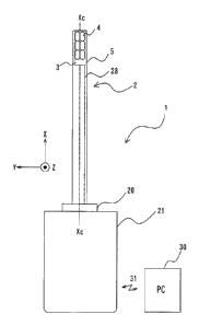
Figure 2 is a top view illustrating a gap sensor
according to an embodiment of the present invention. The
gap sensor 1 has a probe 2 on which electrodes to detect
gaps are arranged and a main body 21 that is connected
through a connector 20 serving as a probe support to the
probe 2. The main body 21 includes a control part 10 that
applies a voltage to the detecting electrodes of the probe 2
and measures displacement currents. The
probe 2 has an
elongated shape extending in the direction of a main axis
(Xc) in an XY-plane and is inserted into a gap space G to
measure gaps, the gap space G being formed between opposing
surfaces Si and S2 of conductive members such as works. The
probe 2 has a flexible printed board 5 provided with an
electrode part 3 that includes an array of electrode pairs 4.
The flexible printed board (FPB) 5 in Fig. 1 has an
elongated shape extending in the main axis direction X and a
three-layer structure. The FPB 5 applies a predetermined
potential between the electrodes 4 and the surfaces Si and
S2 of the conductive members to be measured, measures
45-
CA 2989869 2017-12-22
response currents, and according to obtained capacitances,
finds gaps at the positions of the electrodes. The surfaces
of the probe 2 including the electrode part 3 are covered
with a filler film to be attracted by a magnet.
<Probe Electrode>
Structures of conductive faces in the electrode part 3
of the probe 2 are schematically illustrated in Figs. 1(b)
and 3. The flexible printed board (FPB) 5 has a guard
pattern G1 (a first conductive layer Cl) that defines a top
face (a first face) P1, a guard pattern G2 (a third
conductive layer C3) that defines a bottom face (a second
face) P2, and a signal pattern Es (a second conductive layer
C2) that is held between the two guard patterns. The signal
pattern Es is an aggregate of electrode signal patterns Esi
that are electrically separately connected to electrodes Ei.
Among the conductive layers, insulation layers (not
illustrated) are arranged. In Fig. 1(b), the electrodes Ei
are illustrated circular for convenience. They may have an
optional shape such as oval and ellipse.
Referring to Fig. 3, the electrode part 3 includes an
electrode pattern El that is formed in the first conductive
layer Cl and is surrounded by the guard pattern Gl. Between
the electrode pattern El and the guard pattern Gl, an
annular gap gpl is formed to serve as an insulator, and
therefore, the electrode pattern El and guard pattern G1 are
not electrically connected to each other. An electrode
pattern E2 is formed in the third conductive layer C3 and is
surrounded by the guard pattern G2. Between the electrode
pattern E2 and the guard pattern G2, an annular gap gp2 is
formed, and therefore, the electrode pattern E2 and guard
pattern G2 are not electrically connected to each other.
CA 2989869 2017-12-22
The electrode patterns El and E2 are formed at the same
position in the XY-plane and constitute an electrode pair.
In the second conductive layer C2, a guard pattern Ge
is formed at a position corresponding to the electrode pair
and is electrically connected through via holes Gbl and Gb2
to the guard patterns G1 and G2, respectively. On the other
hand, the electrode pattern El is connected through a via
hole Ebl to a corresponding signal pattern Esl of the second
conductive layer C2 and the electrode pattern E2 is
connected through a via hole Eb2 to a corresponding signal
pattern Es2. In the second conductive layer C2, gaps are
formed between the via holes Ebl and Eb2 and the guard
pattern Ge. A plurality of electrode pairs are formed in
the electrode part 3 and the electrodes Ei are connected
through the signal patterns Esi to corresponding voltage
clamp amplifiers VCAi, respectively.
The guard patterns Gl, Ge, and G2 are common to all
electrodes (Ei: i = 1, 2, ..., n) (n being the number of the
electrodes 4). Accordingly, as will be explained later, all
of the electrodes Ei are separately and independently
voltage-clamped by the same probe signal Vp, and at the same
time, the guard patterns Gl, Ge, and G2 are driven by the
probe signal Vp, so that all electrodes are always at the
same potential. All of the electrodes Ei and guard patterns
are electrically independent of one another, and therefore,
are in a virtual short-circuited state but not actually
short-circuited. Due to this, the three-layer structure is
able to precisely measure capacitances. The electrodes Ei
are separately voltage-clamped, and therefore, it is
possible to simultaneously measure their clamp currents and
simultaneously obtain capacitances. The embodiment
illustrated in Fig. 2 will be explained on an assumption
-8-
CA 2989869 2017-12-22
that it has six electrode pairs, i.e., the number of
electrodes is twelve (n - 12).
<Equipotential Drive Control>
Figure 4 is a schematic view illustrating a control
circuit of the control unit 10. Controlling guard potential
and electrodes according to the present invention uses an
original equipotential driving technique. A probe signal
generator SG generates a sinusoidal wave as a reference
probe signal Sp. The amplitude thereof is controlled by a
microcontroller MC. The probe signal Sp is transmitted
through a driver AMP and is applied as a guard signal Vp to
the guard patterns Gl, Ge, and G2.
The voltage clamp amplifiers (voltage clamp circuits)
VCA1 to VCA12 are connected through the signal patterns Esl
to Es12 to the 12 electrodes El to E12, respectively. Each
voltage clamp amplifier VCAi receives the output Vp of the
driver AMP as a probe voltage to voltage-clamp the electrode
Ei at the voltage Vp. The probe voltage Vp is a sinusoidal
wave, and therefore, the voltage clamp amplifier VCAi is a
variable voltage source.
The voltage clamp amplifier VCAi includes a main clamp
amplifier OPia, i.e., a differential amplifier (operational
amplifier). When receiving the probe voltage Vp at a non-
inverting input terminal (+), the main clamp amplifier OPia
conducts negative feedback control to always equalize a
clamp output voltage Vfia connected to an inverting input
terminal (-) with the probe voltage Vp. Between an output
terminal of the main clamp amplifier OPia and the inverting
input terminal thereof, a resistor (clamp current detecting
resistor) Rsia is connected to detect a clamp current Isi.
A terminal voltage of the resistor Rsia is able to provide a
-9-
CA 2989869 2017-12-22
clamp current (displacement current) at the time of voltage-
clamping of the electrode El.
The terminal voltage AV of the resistor Rsia is
detected through selector switches SW1 and SW2 and is
amplified by a differential amplifier INA to provide the
clamp current Iei = AV / Rsia.
The main clamp amplifier OPia is a differential
amplifier that slightly involves an input capacitance, a
bias current, and the like, as well as temperature
characteristics and characteristic variations. The
capacitance of a measuring object is generally about pF or
lower, and therefore, the characteristic variations of the
differential amplifier may cause large measurement errors.
To deal with this, a differential amplifier of equal
characteristics is employed as a reference clamp amplifier
OPib to compensate for error elements other than the probe
current.
More precisely, the voltage clamp amplifier VCAi has,
in addition to the main clamp amplifier OPia, the reference
clamp amplifier OPib. The reference clamp amplifier OPib
has an external circuit that is the same as that of the main
clamp amplifier OPia. Receiving the prove voltage Vp at a
non-inverting input terminal (+), the reference clamp
amplifier OPib conducts negative feedback control to always
equalize a clamp output voltage VFib with the probe voltage
Vp. The clamp output voltage Vfib has no load element
because it is not connected to the electrode El. This is
the only difference from the main clamp amplifier OPia.
Between an output terminal of the reference clamp
amplifier OPib and an inverting input terminal thereof, a
resistor (reference current detecting resistor) Rsib is
connected to detect a clamp current In for no load
CA 2989869 2017-12-22
condition. A terminal voltage of the resistor Rsib is able
to provide a reference clamp current In at the time of
voltage clamping under no load condition. The reference
clamp current In reflects current components other than a
current passing through load, i.e., the electrode. On the
other hand, clamp output voltages Vfia and Vfib of the two
operational amplifiers are substantially equal to the probe
voltage Vp at the time of voltage clamping. Accordingly, a
probe voltage Voia detected by the main clamp amplifier OPia
is understood to involve the bias current In relating to
the differential amplifier in addition to the net clamp
current Isi. Accordingly, a differential computation
between the output voltages Voia and Voib of the main and
reference clamp amplifiers OPia and OPib is able to provide
a net clamp current Iei.
The two differential amplifiers OPia and OPib that
form the voltage clamp amplifier VCAi are preferably
operational amplifiers having equal characteristics and
packed in one package to form a dual-type operational
amplifier. To protect inputs to the differential amplifiers,
a resistor may be inserted between each non-inverting input
terminal and each of the clamp output terminals Vfia and
vfib.
According to the embodiment of Fig. 4, the
microcontroller MC controls the selector switches (analog
switches) SW1 and SW2 to sequentially select a measuring one
from the electrodes Ei, and the differential amplifier
(instrumented amplifier) INA carries out a differential
computation between the output voltages Voia and Voib,
thereby precisely detecting a clamp current to serve as a
current detecting circuit.
The present invention employs the equipotential
-11-
CA 2989869 2017-12-22
driving technique to separately drive electric elements by
the same potential, and therefore, is capable of, in
principle, simultaneously measuring clamp currents of a
plurality of electrodes. The present embodiment combines
one differential amplifier INA with selector switches to
measure electrode capacitances in time division. Employing
one processing system commonly for all electrodes may
realize stabilized processing and compactness of the main
body 21. According to the present embodiment, the probe 2
has twelve electrodes in six pairs. It is possible to
employ a larger number of electrodes.
<Feedback Control of Adaptive Probe Signal and Charge Clamp
Technique>
The electrode Ei is a flat electrode and forms a
virtual capacitor (capacitance C) with respect to an
opposing surface to be measured. By measuring the
capacitance, a distance d between the electrode and the
surface can be found as will be explained later.
When a potential difference v occurs between the
electrode Ei and the conductive surface Si or S2, the
surface causes a charge q - Cv. If
the potential
difference is of an alternating current, a displacement
current i - Cgv / 61 passes through the electrode. The
conductive surface in the same area as the electrode shows a
charge of the opposite polarity, and therefore, there is a
relationship of C = ES / d where d is the distance between
the electrode and the conductive surface and 8 is a
permittivity of a gap space. Accordingly, measuring the
displacement current and finding therefrom the capacitance
of the virtual capacitor results in obtaining the distance d
- ES/C. According to the present embodiment, the potential
12-
CA 2989869 2017-12-22
difference v is controlled by voltage clamp as mentioned
above so that it correctly agrees with the probe signal Vp
which is expressed as Vp(t) = Asin(2nft).
The amplitude of a clamp current created by an applied
probe signal becomes smaller as the capacitance C of a
measuring object becomes smaller, to lower a detection
accuracy. To deal with this, the present embodiment
maintains the amplitude of a clamp current at around a
predetermined level by making the microcontroller MC
adaptively control the amplitude A of a probe signal,
thereby improving the measurement accuracy. Keeping the
amplitude of a current constant corresponds to keeping an
accumulated charge as an integral value of displacement
current constant irrespective of variations in the capacitor
capacitance. More precisely, if the amplitude of a clamp
current becomes smaller, the microcontroller MC increases
the amplitude of the probe signal Vp serving as a common
potential for the equipotential driving, and if the
amplitude of the clamp current becomes larger, decreases the
amplitude of the probe signal Vp.
It is more preferable to feedback-control the prove
signal voltage Vp in such a way as to keep constant the
amplitude of a clamp current that is proportional to a
voltage amplitude coefficient A, so that a capacitance is
obtained from an amplitude A of the adaptive probe signal Vp.
This is to feedback-control the magnitude of the probe
signal Vp in such a way as to charge the virtual capacitor
constituted by the measuring object and electrode to a
predetermined capacitance. This is an original charge clamp
technique of the present invention based on the electrode
voltage clamp control and equipotential driving control.
According to the charge clamp technique of the present
-13-
CA 2989869 2017-12-22
invention, when the probe signal voltage Vp has an amplitude
AO with respect to a known corrected reference capacitance
CO and when the adaptive probe signal voltage Vp has an
amplitude A with respect to an optional capacitance C, there
is established a relationship of C/CO = A/AO. Information
about the amplitude A is directly obtainable by rectifying
and smoothing (integrating) the probe signal Vp.
Accordingly, only by measuring the amplitude A of the
adaptive probe signal voltage Vp under feedback control, the
capacitance C can be measured.
According to the present embodiment, the probe signal
Vp is a sinusoidal wave. This does not limit the present
invention. Any waveform is adoptable. Even in such a case,
a capacitance can be obtained from a magnitude of the probe
signal voltage Vp needed to charge a predetermined
capacitance.
The configuration of the electrode part of the probe
and the voltage clamp control, equipotential driving control,
and charge clamp control according to the present invention
always drive the guard electrodes and all electrodes with a
voltage equal to the probe signal Vp. During the voltage
clamp operation, the potential of an electrode whose clamp
current is being detected is fixed to the probe signal, and
therefore, it is possible to highly stably and precisely
measure a gap. A plurality of differential amplifiers INA
may be arranged to simultaneously obtain clamp currents from
a plurality of electrodes.
<Gap Measurement>
A gap measuring method employing the gap sensor
according to the present invention will be explained.
Electrodes Ei of each pair in the electrode pair array
14-
CA 2989869 2017-12-22
4 of the probe 2 are arranged on the top face P1 and bottom
face P2, respectively, at the same position on the substrate
and are separately connected through the signal lines Es
to the control unit 10 incorporated in the main body 21.
5 As illustrated in Fig. 5, the probe 2 is inserted into
the gap G and each electrode pair detects capacitances at
the position, to obtain a capacitance between the upper
electrode El and the surface Si, and then, a capacitance
between the lower electrode E2, which is at the same
position as the upper electrode El, and the surface S2.
Based on the capacitance data, a distance dl between the
upper electrode El and the surface S1 and a distance d2
between the lower electrode E2 and the surface S2 are
obtained. It is then possible to find a gap d between the
opposing surfaces Si and S2. For each of the electrode
pairs, a similar measurement is successively carried out to
obtain a two-dimensional distribution of gaps d over the
electrode part. The gap data obtained by the gap sensor 1
is transmitted through a communication unit 31 to a
controller 30 that processes the data.
The electrode pairs 4 are discretely arranged on the
probe 2. Since a plurality of electrode pairs are arranged,
positions of the electrode pairs and gap data are usable to
compute data relating to an optional position among adjacent
electrode pairs. For example, gap data of adjacent three
electrode pairs 4 may be complemented each other to obtain
gap data of an optional position in an area surrounded by
the electrode pairs in question. As a result, the
embodiment reduces the size of the gap sensor and is able to
continuously measure a wide gap space and three-
dimensionally displaying the gap space. The probe 2 is
provided with a scale 28 in the direction of the main axis
-15-
CA 2989869 2017-12-22
Xc, and therefore, it is easy to confirm the position
(depth) r of a measuring electrode Ei.
It is assumed that a measuring object whose gap is
measured is made of conductive material such as aluminum
alloy and carbon fiber. Even if it is made of nonconductive
material, a gap measurement is possible if the surfaces
thereof are coated or covered with conductive material.
When measuring gaps, it is preferable that electrode
surfaces are in parallel with the measuring surfaces Si and
S2. As illustrated in Fig. 6(a), a magnet 25 may be used to
attract the probe 2 to the measuring surface Si. The
surface of the probe 2 is provided with a magnetic filler
film, and therefore, arranging the magnet 25 to attract the
probe 2 toward the measuring surface Si realizes a more
stable gap measurement.
The present invention employs the original electrode
structure and measures capacitances with the use of the
equipotential driving technique and charge clamp control,
thereby improving the correctness and reproducibility of a
measurement of gaps. The equipotential driving technique
according to the present invention uses a probe signal as a
common potential, and therefore, is effective not only to
the three-layer substrate structure of the embodiment but
also to any other structure involving a plurality of
electrodes and guard patterns driven by a common potential.
When conducting a gap measurement, the gap sensor 1
must be calibrated. For the calibration, a reference sample
made of aluminum flat plate and having predetermined gaps dO
is used. The predetermined gaps are, for example, 0.5 mm, 1
mm, 2 mm, and 3 mm. The metal flat plate and gap sensor 1
are commonly grounded. Into a gap G of the reference sample,
the probe 2 is inserted to measure and correct the gaps dO.
16-
CA 2989869 2017-12-22
The correction includes correcting the above-mentioned
reference amplitude AO and the like.
<Other Embodiments>
Figures 7 and 8 illustrate a probe 2 according to
another embodiment. The structure of an electrode part
thereof is the same as that of the probe 2 of the embodiment
illustrated in Fig. 2. However, electrode pairs 4a to 4h
are arranged along a main axis Xc of the probe 2 in two
zigzag lines and include 16 circular electrodes. The probe
2 is fixed to a main body 21 through a probe support unit
(including a connector) 20 that has a rotary shaft turnable
around an axis Y. If an upper member such as a work is a
plate member, the main body 21 is set on a top surface of
the plate member and the probe 2 is folded toward a bottom
face 21B and inserted into a gap G. The probe support unit
is vertically movable depending on the thickness of the
plate member. As illustrated in Fig. 6(b), the bottom of
the main body 21 incorporates a magnet 25 to attract the
20 probe 2 to a surface S1 due to magnetism of a filler film of
the probe 2.
A gap measurement is carried out as explained above by
conducting the charge clamp control that applies a probe
signal Vp to equalize a guard potential and the potential of
every electrode and measures capacitances between upper and
lower electrodes of each electrode pair 4 to obtain data
about a gap d. The gap measurement is successively carried
out on all of the electrode pairs 4.
Arranged on the bottom face 213 are a rotary encoder
23 serving as a position detecting sensor to measure a
moving distance (a relative position) in the direction Y and
a reference position detecting sensor 24 to confirm a
17-
CA 2989869 2017-12-22
reference position in the direction Y. Arranged at regular
intervals in the direction Y on the top surface of the plate
member are barcode markers that are detected by the
reference position sensor 24. The reference position
detecting sensor 24 reads reflected light from the markers
and detects a reference position. According to this
embodiment, the probe 2 is turned to be in parallel with the
bottom face 21B of the main body 21. For a gap extending in,
for example, a YZ-plane, the probe 2 may be turned to be in
parallel with an axis Z to enable a gap measurement.
According to the present invention, the probe has a
three-layer structure and the electrodes are provided with
common guards, to realize a thin configuration to measure
narrow gaps. The guards are set to a common potential to
reduce the number of wires and increase the number of
electrodes to be arranged on a probe. The equipotential
driving control drives all electrodes and guards to an equal
potential to realize a stable and reproducible measurement.
The charge clamp technique enables a capacitance to be
measured from the magnitude of a probe signal.
(United States Designation)
In connection with United States designation, this
international patent application claims the benefit of
priority under 35 U.S.C. 119(a) to Japanese Patent
Application No. 2017-104083 filed on May 26, 2017 whose
disclosed contents are incorporated herein by reference.
18-
CA 2989869 2017-12-22