Note: Descriptions are shown in the official language in which they were submitted.
CA 02990879 2017-12-27
WO 2017/001258
PCT/EP2016/064401
1
METHOD OF MANUFACTURING A CAPACITIVE ELECTRICAL
DEVICE
TECHNICAL FIELD
The present disclosure generally relates to electrical devices such as
transformers and bushings. In particular, it relates to method of
manufacturing a capacitive electrical device.
BACKGROUND
Electrical devices, such as bushings, cable terminations, and measurement
to transformers, and capacitors may comprise capacitive electrical devices.
Capacitors, for example, may comprise a conductive layer wound around a
shaft together forming a capacitive electrical device. The conductive layer is
insulated from another conductive layer by means of an electrical insulator
such as an insulating film.
Bushings may comprise a condenser core forming the capacitive electrical
device. The condenser core comprises a plurality of conductive layers
electrically insulated from each other and extending longitudinally along the
electrical device body. In order to improve the electrical withstand strength,
the axial length of each conductive layer is shorter than that of the
corresponding insulation layers between which a conductive layer is
sandwiched.
For large electrical devices the width of the films forming the electrical
insulation available on the market may be less than that required by the
electrical device. In this case it may be necessary to joint several films or
sheets forming the electrical insulation of the capacitive electrical device.
One
known method of jointing insulating films is by winding films together with
an overlap. This overlap creates areas of double film thickness at the joint.
Further, this creates areas with high risk of voids and cavities in the
vicinity
of the overlap joint. This in turn reduces the dielectric strength in the
joint
CA 02990879 2017-12-27
WO 2017/001258
PCT/EP2016/064401
2
area and/or may create partial discharges in service. Such a lap joint will
make it difficult or impossible to make a sufficiently homogeneous condenser
core of laminated films.
Another method that is utilised today for jointing involves placing papers or
other porous films with an overlap and cut the paper in the overlap and
removing the excess material, then impregnate the condenser core with an
impregnation liquid in a vacuum impregnation process that fills up the
cavities, inhomogeneities, and clefts with the fluid. The fluid can also be of
the type that solidifies by a curing process, e.g. a resin. This method
requires
a substantial amount of time for the impregnation and curing process, which
increases the manufacturing costs.
GB 1 129 995 A discloses a method of manufacturing an electric insulating
bushing. The bushing is made by winding side-by-side on to a former or the
like at least two sheets of flexible insulating material, e.g. paper, which
initially overlap a distance W and are then cut by a reciprocating cutter in
this
overlapping region as they are fed forward together on to the former to
produce complementary abutting serrated or tapered edges. Layers of foil
may be interleaved with the insulating sheeting to reduce electric stress. The
insulation may be increased by impregnating the bushing material with, for
example, an insulating oil or gas, or a plastics resin that may be cured
during
fabrication of the bushing by using heated rollers.
DE 27 57 256 Ai discloses coaxial insulation for a cable and uses a signal
inner conductor, or a rigid inner tube round a flexible inner conductor, as a
winding mandrel for insulation tape, or web. Several such insulating webs are
continuously applied to the winding mandrel in overlapping manner. The
overlaps of two adjacent webs are so trimmed, prior to contacting the winder,
as to form a narrow gap, between two adjacent webs. The winding mandrel
and the web cutting device can be axially shifted, when one of them is
stationary. Thus the gaps in individual lengths are covered. Alternately gaps
in several layers may be covered by the top one.
CA 02990879 2017-12-27
WO 2017/001258
PCT/EP2016/064401
3
GB 1 339 259 A discloses a method of manufacturing a bushing where two
lengths of insulating sheet material are wound around a former. This
document aims to manufacture a bushing in which the axial length of the
insulator substantially exceeds the width of the paper or other insulating
sheet material used. The figure below shows that the two pieces of insulation
ii and 12 are arranged in an overlapping manner forming overlaps 15 and 16,
wherein a cutter 17 cuts the overlapping portion as the insulation is rolled
onto the former 13. In this way the adjacent obliquely severed straight edges
of the two lengths of paper will be laid in edge-to-edge abutted relationship,
forming a butt joint of helical spiral form and of constant axial pitch. The
completed bushing insulator may be impregnated may be impregnated by a
vacuum process with a liquid casting resin, which when cured will bond the
turns of the paper winding together.
SUMMARY
An object of the present disclosure is to provide a method of manufacturing a
capacitive electrical device with jointed films which solves or at least
mitigates existing problems of the state of the art.
Hence, according to a first aspect of the present disclosure there is provided
a
method of manufacturing a capacitive electrical device, wherein the method
comprises: a) bonding a first electrical insulation film with a second
electrical
insulation film to obtain a single electrical insulation film that has a
larger
surface area than any of the first electrical insulation film and the second
electrical insulation film has alone, b) providing a conductive layer onto the
single electrical insulation film, and c) winding the single electrical
insulation
film and the conductive layer around a shaft to obtain a layer of the single
electrical insulation film and a layer of the conductive layer wound onto the
shaft, thereby forming the capacitive electrical device.
By means of the jointing process in which the first electrical insulation film
and the second electrical insulation film are bonded to form a single
electrical
insulation film prior to them being wound around the shaft. By means of
bonding, a capacitive electrical device without any significant
CA 02990879 2017-12-27
WO 2017/001258
PCT/EP2016/064401
4
inhomogeneities or voids may be created. The joint can be created during the
winding process without any post-processing of the condenser core. No
impregnation process is necessary to obtain a single electrical film with
essentially uniform dielectric properties of the single electrical insulation
film, also in the joint between the first electrical insulation film and the
second electrical insulation film.
One embodiment comprises, prior to step a), placing a first edge of the first
electrical insulation film and a second edge of the second electrical
insulation
film towards each other to obtain a slot between the first electrical
insulation
film and the second electrical insulation film, wherein step a) involves
applying a bonding agent into the slot and onto the first edge and the second
edge to thereby bond the first electrical insulation film to the second
electrical insulation film.
One embodiment comprises, prior to step b), removing excessive bonding
agent material from the surfaces of the single electrical insulation film.
According to one embodiment step a) involves moving an injection tool
parallel with the slot along the entire first edge and the entire second edge,
wherein the bonding agent is provided into the slot by the injection tool as
the injection tool moves relative to the first electrical insulation film and
the
second electrical insulation film, along the entire first edge and the entire
second edge.
According to one embodiment the placing involves placing the first electrical
insulation film and the second electrical insulation film on a first roll, and
feeding the first electrical insulation film and the second electrical
insulation
film towards a nozzle by rotating the first roll, wherein step a) involves
applying the bonding agent into the slot by means of the nozzle, and a')
shaping the bonding agent in the slot by rolling the single electrical
insulation
film between the first roll and a second roll.
According to one embodiment the bonding agent is glue or a thermoplastic
material.
CA 02990879 2017-12-27
WO 2017/001258
PCT/EP2016/064401
One embodiment comprises, prior to step a), placing a first end portion of the
first electrical insulation film to overlap a second end portion of the second
electrical insulation film to obtain an overlapping portion, wherein step a)
involves heating the overlapping portion to bond the first electrical
insulation
5 film with the second electrical insulation film.
According to one embodiment the first end portion includes a first edge of the
first electrical insulation film and the second end portion includes a second
edge of the second electrical insulation film, wherein step a) involves moving
a heating tool along the overlapping portion, parallel with and along the
to entire extension of the first edge and the second edge.
One embodiment comprises a step a") of removing excessive material from
the surface of the single electrical insulation film created in step a), prior
to
step b).
One embodiment comprises, after step a), rolling the overlapping portion
between a first roll and a second roll to smoothen the single electrical
insulation film.
According to one embodiment the first roll and the second roll are heated
such that the highest temperature of each of the first roll and the second
roll
is a respective section contacting the overlapping portion.
According to one embodiment step a) involves bonding the first electrical
insulation film with the second electrical insulation film such that the
single
electrical insulation film obtains a longer axial extension than any of the
first
electrical insulation film and the second electrical insulation film alone,
with
the axial extension being defined in the axial direction of the shaft.
According to one embodiment the condenser core is a condenser core for a
medium voltage electrical device or a high voltage electrical device.
According to one embodiment the conductive layer is a conductive foil.
CA 02990879 2017-12-27
WO 2017/001258
PCT/EP2016/064401
6
According to a second aspect of the present disclosure there is provided a
capacitive electrical device obtainable by the method according to the first
aspect.
Generally, all terms used in the claims are to be interpreted according to
their
ordinary meaning in the technical field, unless explicitly defined otherwise
herein. All references to "a/an/the element, apparatus, component, means,
etc. are to be interpreted openly as referring to at least one instance of the
element, apparatus, component, means, etc., unless explicitly stated
otherwise.
BRIEF DESCRIPTION OF THE DRAWINGS
The specific embodiments of the inventive concept will now be described, by
way of example, with reference to the accompanying drawings, in which:
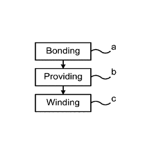
Figs la-c illustrate flow charts of methods of manufacturing a capacitive
electrical device;
Figs 2a-c show a first example of a bonding a first electrical insulation film
with a second electrical insulation film for manufacturing a capacitive
electrical device;
Fig. 3 shows a second example of a bonding of a first electrical insulation
film
with a second electrical insulation film for manufacturing a capacitive
electrical device;
Figs 4a-d show a third example of a bonding of a first electrical insulation
film with a second electrical insulation film for manufacturing a capacitive
electrical device;
Fig. 5 shows a fourth example of a bonding of a first electrical insulation
film
with a second electrical insulation film for manufacturing a capacitive
electrical device;
CA 02990879 2017-12-27
WO 2017/001258
PCT/EP2016/064401
7
Figs 6a-d show a fifth example of a bonding of a first electrical insulation
film
with a second electrical insulation film for manufacturing a capacitive
electrical device; and
Figs 7a-d show a sixth example of a bonding of a first electrical insulation
film with a second electrical insulation film for manufacturing a capacitive
electrical device.
DETAILED DESCRIPTION
The inventive concept will now be described more fully hereinafter with
reference to the accompanying drawings, in which exemplifying
embodiments are shown. The inventive concept may, however, be embodied
in many different forms and should not be construed as limited to the
embodiments set forth herein; rather, these embodiments are provided by
way of example so that this disclosure will be thorough and complete, and
will fully convey the scope of the inventive concept to those skilled in the
art.
Like numbers refer to like elements throughout the description.
The present disclosure relates to a method of manufacturing a capacitive
electrical device. With reference to Fig. la, the method includes a) bonding a
first electrical insulation film with a second electrical insulation film to
create
a single electrical insulation film. The single electrical insulation film has
a
larger surface area than any of the first electrical insulation film and the
second electrical insulation film has alone. To this end, the bonding in step
a)
is a jointing of the first electrical insulation film and the second
electrical
insulation film.
The first electrical insulation film and the second electrical insulation film
are
bonded in such a way that the joint formed between them has essentially the
same thickness as the thickness of any of the first electrical insulation film
and the second electrical insulation film. This essentially uniform thickness
of
the single electrical insulation film may for example be obtained by
mechanically tooling or shaping the joint post bonding, as will be described
in more detail in the following.
CA 02990879 2017-12-27
WO 2017/001258
PCT/EP2016/064401
8
Each of the first electrical insulation film and the second electrical
insulation
film may for example be made of polymer e.g. a thermoplastic film, fibreglass
web, or glass. In particular, the first electrical insulation film and the
second
electrical insulation films may be made of a material or a material
combination which is able to withstand high temperatures developed when in
use.
In a step b) a conductive layer is provided onto the single electrical
insulation
film. The conductive layer may for example be a foil, or it may be a coating
applied to the single electrical insulation film. In the case of a coating,
the
coating may for example be a conductive compound layer such as conductive
ink or conductive polymer, or it may be a metallization layer. The coating
may for example be applied by means of physical vapour deposition, or by
printing by means of a printing device. Such printing technology may for
example be based on screen-printing, ink jet printing, intermittent web
coating or slot die coating.
In a step c) the single electrical insulation film and the conductive layer
which
is provided on the single electrical insulation film are concurrently wound
around a shaft to obtain a layer of the single electrical insulation film and
a
layer of the conductive layer wound onto the shaft. The shaft and the single
electrical insulation film wound around the shaft hence form a capacitive
electrical device.
Examples of capacitive electrical devices obtainable by means of the above-
described process are condenser cores and capacitors. In the case of a
capacitor, the capacitive electrical device may comprise a second conductive
layer electrically insulated from a first conductive layer by means of the
single
electrical insulation film. In this case, in step b) a respective conductive
layer
may be provided on each of the two opposite surfaces of the single electrical
insulation film. In step c) the single electrical insulation film and the two
conductive layers arranged on either side of the single electrical insulation
film may be wound around the shaft.
CA 02990879 2017-12-27
WO 2017/001258
PCT/EP2016/064401
9
In the case the capacitive electrical device is a condenser core, a number of
regions may be provided with a conductive layer on the single electrical
insulation film. Those regions which are not provided with a conductive layer
define electrically insulating regions of capacitive electrical device. The
single
electrical insulation film provided with a number of regions of conductive
layers is wound around the shaft in step c) and thus forms a condenser core.
Thereby a plurality of electrically insulating layers and electrically
conductive
layers are obtained around the shaft.
With reference to Figs th to 7d, a number of examples of how to manufacture
to a capacitive electrical device for an electrical device will be
described in more
detail.
Fig. 2a shows a first example of bonding a first electrical insulation film ta
with a second electrical insulation film tb. In Fig. 2a, the first electrical
insulation film ta and the second electrical insulation film th are placed
with
their edges towards each other. In particular, a first edge 3a of the first
electrical insulation film ta is placed adjacent to and parallel with a second
edge 3b of the second electrical insulation film tb. The first edge 3a and the
second edge 3b are placed at a slight distance from each other such that a
slot
5 is formed between the first electrical insulation film ta and the second
electrical insulation system tb.
In Fig. 2b an injection tool 7 is shown placed around the slot 5 such that the
injection tool can inject a bonding agent into the slot 5, as shown by means
of
arrow A. The injection tool 7 is arranged to move relative to the slot 5,
parallel with the first edge 3a and the second edge 3h, along the entire
length
of the first edge 3a and the entire length of the second edge 3b. For this
purpose, the injection tool 7 could for example be movable along the slot 5
with the first electrical insulation film ta and the second electrical
insulation
film th being spatially still, or alternatively or additionally the first
electrical
insulation film ta and the second electrical insulation film th may be
arranged to move for example by means of feed rolls to obtain relative
movement with respect to the injection tool 7. The first electrical insulation
CA 02990879 2017-12-27
WO 2017/001258
PCT/EP2016/064401
film la and the second electrical insulation film ib, and in particular the
slot 5
could thereby be moved past the injection tool 7 such injection tool 7 can
fill
the slot 5 with the bonding agent.
In Fig. 2c, a single electrical insulation film lc is shown, having been
formed
5 by bonding the first electrical insulation film la and the second
electrical
insulation film ib. The bonding agent thus fills the slot 5, and adheres to
the
first edge 3a and to the second edge 3b. A joint 9 is hence formed between the
first electrical insulation film la and the second electrical insulation film
ib.
The single electrical insulation film lc may then be used in steps b) and c)
to
to manufacture the capacitive electrical device.
The injection tool 7 may have a first part 7a bearing against the first
electrical
insulation film la and the second electrical insulation film ib and arranged
at
one side of the slot 5. The first part 7a has an essentially planar surface
and
forms a floor for the slot 5. The injection tool 7 also has a second part 7b
arranged at the opposite side of the slot 5. The second part 7b includes a
runner into which the bonding agent may be injected. The bonding agent that
has been provided into the slot 5 is shaped as the injection tool 7 moves
relative to the films la and ib along the slot 5. In this way the single
electrical
insulation film lc created by jointing of the films la and ib may obtain an
essentially uniform thickness.
With reference to Fig. 3 a second example of bonding a first electrical
insulation film la with a second electrical insulation film ib is shown.
According to this example, the first electrical insulation film ib is placed
with
its first edge 3a towards the second edge 3b of the second electrical
insulation
film ib such that a slot 5 is created between the first electrical insulation
film
la and the second electrical insulation film ib. The first electrical
insulation
film la and the second electrical insulation film ib are placed on a first
roll Ri
which feeds the two films la and ib forward towards a nozzle ii. The nozzle ii
is essentially as wide as the combined width of the two films la, ib when
placed beside each other on the first roll Ri. A second roll R2 is arranged
adjacent to the first roll Ri such that a small gap 13 is created between the
CA 02990879 2017-12-27
WO 2017/001258
PCT/EP2016/064401
11
first roll Ri and the second roll R2. The gap 13 is just large enough that the
films la and ib can pass through. The nozzle 11 is placed above the gap 13
between the first roll Ri and the second roll R2. The nozzle 11 is arranged to
deliver a bonding agent B into the slot 5 and onto the first electrical
insulation film la and the second electrical insulation film 113, as the films
la
and 113 move into the gap 13 and are pressed between the first roll Ri and the
second roll R2. The first roll Ri and the second roll R2 rotate in opposite
directions and the single electrical insulation film lc created by the bonding
of the two films la and 113 by means of the bonding agent B may be rolled
onto the second roll R2.
The nozzle can alternatively be placed with an offset from the gap 13, above
either the first roll Ri or above the second roll R2. Thereby the heated
liquid
bonding agent B discharged from the nozzle may be allowed to slightly cool
before reaching the gap 13. Any dripping of the bonding agent B applied to
the first film la and the second film 113 may thereby be reduced.
The single electrical insulation film lc is shaped in a step a') by means of
the
first roll Ri and the second roll R2 when fed between these rolls. A
conductive layer may be provided onto the single electrical insulation film lc
obtained in this manner in step b) and wound onto a shaft to form a
capacitive field gradient device in step c). In particular, the conductive
layer
may advantageously be provided by means of printing or spraying. The
conductive layer can for example be applied as the single electrical
insulation
film lc is rolled onto the second roll R2. For this purpose, a conductive
layer
application device may be arranged to the right of the second roll R2 in Fig.
3.
According to one variation, the second roll R2 may be the shaft of the
capacitive electrical device created in the process described in Fig. 3. The
second roll R2 may thus be removed when the single electrical insulation film
lc has been fully wound around the second roll R2.
Figs 4a-d show a third example of bonding a first electrical insulation film
la
with a second electrical insulation film 113. The first electrical insulation
film
CA 02990879 2017-12-27
WO 2017/001258
PCT/EP2016/064401
12
la and the second electrical insulation film lb are placed beside each other
with the first edge 3a facing the second edge 3b as has been described above.
An injection tool 7' is placed around the slot 5 formed between the first
electrical insulation film la and the second electrical insulation film ih.
The
injection tool 7' has a cavity 15 into which a bonding agent may be provided
in order to fill the slot 5 with the bonding agent to thereby form a single
electrical insulation film. The injection tool 7' is movable parallel to the
first
edge 3a and the second edge 3b, along the entire extension of the first edge 3
a
and the entire extension of the second edge 3b. The injection tool 7' may be
moved along the slot 5 or the films la, lb may be arranged to move while the
injection tool 7' is arranged spatially fixed.
In Fig. 4c, a single electrical insulation film lc has been obtained by means
of
the bonding process shown in Fig. 4h. Excessive bonding agent material 17
present after the bonding step may be removed from the surfaces of the
single electrical insulation film lc. In this manner an essentially uniformly
thick single electrical insulation film lc may be obtained, as shown in Fig.
4c.
Fig. 5 shows a fourth example of bonding the first electrical insulation film
la
with the second electrical insulation film lb. This example is similar to the
second example, except that the nozzle 11' is narrower and the single
electrical insulation film lc formed by the bonding process is further fed
forward when it has passed between the first roll Ri and the second roll R2.
The narrower nozzle ii' applies the bonding agent B to the slot 5, wherein
most of the applied bonding agent B is limited to being distributed in the
vicinity of the slot 5. The amount of bonding agent B is adapted to minimise
the amount of spill.
A conductive layer may be provided onto the single electrical insulation film
lc, and the single electrical insulation film lc and the conductive layer may
be
rolled concurrently onto a shaft to form a capacitive electrical device in
steps
b) and c).
CA 02990879 2017-12-27
WO 2017/001258
PCT/EP2016/064401
13
The nozzle can according to one variation be placed with an offset from the
gap, above either the first roll Ri or above the second roll R2. Thereby the
heated liquid bonding agent B discharged from the nozzle may be allowed to
slightly cool before reaching the gap 13. Any dripping of the bonding agent B
applied to the first film la and the second film 113 may thereby be reduced.
According to one variation, the arrangement for jointing includes an endless
belt onto which the first electrical insulation film la and the second
electrical
insulation film lb is placed prior to being bonded together. The path of the
endless belt is schematically shown by means of the loop formed by the
dashed lines in Fig. 5. The endless belt provides support for the first
electrical
insulation film la, the second electrical insulation film lb, and also to the
single electrical insulation film lc once the two films la and 113 have been
joined. It may thereby be ensured that the first electrical insulation film la
and the second electrical insulation film lb are bonded together properly.
Figs 6a-d shows a fifth example of bonding a first electrical insulation film
la
with a second electrical insulation film lb. A first end portion 19a of the
first
electrical insulation film la is placed to overlap a second end portion 1913
of
the second electrical insulation film 113 to obtain an overlapping portion
19c.
In this case step a) involves heating the overlapping portion 19c to bond the
first electrical insulation film la with the second electrical insulation film
lb.
For this purpose a heating tool 21 may be used. The heating tool 21 may be
moved along the overlapping portion 19c, parallel with and along the entire
extension of the first edge 3a and the second edge 3b. In this manner the
first
electrical insulation film la and the second electrical insulation film lb may
be welded together by means of the heating tool 21. The resulting single
electrical insulation film lc may become deformed by the heating procedure.
To this end, excessive material 23 is in a step a") removed from the surface
of
the single electrical insulation film la created in the above-described step
a)
of bonding prior to step b) is performed.
CA 02990879 2017-12-27
WO 2017/001258
PCT/EP2016/064401
14
According to one variation, in use the heating tool 21 may have a temperature
gradient which increases towards that portion which is arranged to heat the
overlapping portion 19c.
Figs 7a-d shows a sixth example of bonding a first electrical insulation film
ta
with a second electrical insulation film tb. This example is similar to the
fifth
example, except that after bonding the single electrical insulation film ta is
shaped by means of a first roll Ri and a second roll R2. In particular, the
overlapping portion 19c is fed between the first roll Ri and the second roll
R2
to smooth out the single electrical insulation film tc. A more uniform
to thickness of the single electrical insulation film ta may thereby be
obtained.
According to one variation of the sixth example the first roll Ri and the
second roll R2 may be heated such that the highest temperature of each of the
first roll Ri and the second roll R2 is a respective section contacting the
overlapping portion 19c. Hereto, each of the first roll Ri and the second roll
R2 may have a heat gradient which increases e.g. towards the middle where
they are contacting the overlapping portion 19c.
In any example disclosed herein, the bonding agent may for example be a
glue or a thermoplastic material. Removal of excessive bonding material, or
excessive material, resulting from the bonding step may for example be
performed by ablation, e.g. laser ablation, a mechanical removal process,
thermal melting or combinations of different removal techniques.
By means of the examples of manufacturing the capacitive electrical device
disclosed herein the joint formed between the films ta and 113 may have
essentially the same thickness as the rest of the single electrical insulation
film. This results in a lower risk of voids and thus increases the dielectric
withstand strength of the single electrical insulation film.
The capacitive field gradient device may in particular be suitable for
electrical
devices such as bushings, cable terminations, measurement transformers and
capacitors. The capacitive field gradient device may be suitable for medium
voltage or high voltage applications, for example high voltage direct current
CA 02990879 2017-12-27
WO 2017/001258
PCT/EP2016/064401
(HVDC) applications. Example voltages are from 1 kV to over woo kV, for
example 10 kV and above.
The inventive concept has mainly been described above with reference to a
few examples. However, as is readily appreciated by a person skilled in the
5 are, other embodiments than the ones disclosed above are equally possible
within the scope of the inventive concept, as defined by the appended claims.