Note: Descriptions are shown in the official language in which they were submitted.
INLAY DESIGNS FOR UHF RFID TAGS
FIELD
The present specification relates generally to identification tags using Radio
Frequency
identification (RFID) technology. More specifically the present specification
relates to creation of a
round ultra-high frequency (UHF) wire inlay for use in RFID tags.
BACKGROUND
RFID systems which as such were being used in a wide range of applications
such as retail
supply chain, postal logistics, healthcare, manufacturing etc., have now also
been put to the sector of
animal / livestock management (including industrial purposes and asset
tracking). Ti the animal/live
stock management sector, the RFID system is used to facilitate the
identification and tracking of animals
that need to be reliably monitored and/or controlled within a particular
environment.
The introduction of RFID into these applications has resulted in a more
secure, efficient and
accurate system of the management of the animals / live stock. The objective
of using these systems is
to trace and track every individual animal from birth to the slaughter house
(or as per the requirements
from a particular animal, for example, cow in a milk farm for extraction of
milk) with its individual
information (for example personal identification number, birth, vaccination
etc).
An enabled RFID UHF animal tag is a technology whereby a UHF inlay has been
embedded
into a standard animal tag. RFID is contactless technology, which uses air
interface (electromagnetic
waves) to communicate with the environment. Several common frequencies
1
Date Recue/Date Received 2023-01-19
CA 02991561 2018-01-05
WO 2017/006350
PCT/1N2016/050223
(LF, HF, UHF) are used worldwide, and depending on the application the
appropriate frequency
is chosen. This is because LF, HF and UHF have their own strengths and
weaknesses. Generally
the standard technology used for animal ear tag systems is LF. The inlays used
in the UHF RFID
animal ear tags until now were either machine inlays, printed inlays or etched
inlay which as
such have a restricted read range.
Hence, there is a need in the art for UHF RFID tags having an improved read
range
without compromising on the accuracy of the signals being read.
SUMMARY
In an embodiment the present specification provides an ultra-high frequency
(UHF) radio
frequency identification (RFID) device, comprising: a wire inlay bonded with a
plastic material;
and, an electronic integrated circuit attached thereto. In an embodiment, the
wire inlay is formed
by looping and embedding the wire in a predefined circular design on a
substrate.
In an embodiment, the UHF RFID device operates within frequencies ranging from
840
MHz to 960 MHz. In an embodiment, the electronic integrated circuit comprises
a transponder
chip operating at frequencies ranging from 840 MHz to 960 MHz. In an
embodiment, the
transponder chip is a Class 1 Generation 2 UHF RFID transponder chip.
In an embodiment, the UHF RFID device further comprises an antenna coupled
with an
Interrogator for powering the transponder chip. In an embodiment, the
substrate is made of one
of polyvinyl chloride (PVC), PC, and Polyethylene terephthalate Glycol (PETG).
In an embodiment, the circular design comprises a first portion comprising one
or more
semi-circular loops of wire coupled with a second identical portion comprising
one or more
semi-circular loops of wire; the first and the second portions being separated
by a gap of
predefined dimension. In an embodiment, the transponder chip is positioned
within the gap
between the first and the second portions of the circular design of the wire.
2
CA 02991561 2018-01-05
WO 2017/006350
PCT/1N2016/050223
In an embodiment, a thickness of the wire ranges from 30 American Wire Gauge
(AWG)
to 42 AWG; and an outer diameter of the circular design ranges from 22 mm to
30 mm and an
inner diameter of the circular design ranges from 8 mm to16 mm. In an
embodiment, the plastic
material is Polyvinyl chloride (PVC).
In another embodiment the present specification provides an ultra-high
frequency (UHF)
radio frequency identification (RFID) device, comprising: a wire inlay bonded
with a plastic
material; and, an electronic integrated circuit attached thereto, the device
being placed within to
form a UHF RFID tag. In an embodiment, the tag comprises two halves opening to
receive the
device, the two halves being sealed to form the UHF RFID tag; and the tag is
made of a plastic
or thermoplastic material
The aforementioned and other embodiments of the present shall be described in
greater
depth in the drawings and detailed description provided below.
BRIEF DESCRIPTION OF THE DRAWINGS
These and other features and advantages of the present invention will be
appreciated, as
they become better understood by reference to the following detailed
description when
considered in connection with the accompanying drawings, wherein:
FIG. lA illustrates a circular inlay design for a UHF RFID tag, in accordance
with an
embodiment of the present specification;
FIG. 1B illustrates a UHF transponder/chip fitted in a gap in the circular
inlay design of
the UHF RFID tag in accordance with an embodiment of the present
specification;
FIG. 1C illustrates wire specifications for an inlay design of a UHF RFID tag,
in
accordance with an embodiment of the present specification; and
3
CA 02991561 2018-01-05
WO 2017/006350
PCT/1N2016/050223
FIG. 2 illustrates the stages of employing a UHF wire inlay into an RFID tag,
in
accordance with an embodiment of the present specification.
DETAILED DESCRIPTION
The present specification provides a wire inlay for use in UHF RFID tags as
opposed to a
machine (printed) inlay being used in currently available UHF RFID tags. In
various
embodiments, wires (wire inlay) are embedded on a substrate in a predefined
circular design by
using mechanical processes. The embedded wires are connected to a
transponder/chip resulting
in a much extended read range as compared to the prior art RFID tags. For
example, in an
embodiment, a wire based 30 millimeters(mm) tag provides a read range of 1.5
meters to 2.0
meters whereas a prior art RFID based 30 mm tag provided a read range of about
0.3 meters to
0.7meters.
In an embodiment, the wire inlay is fabricated upon a substrate such as but
not limited to
Polyvinyl chloride (PVC), and Polyethylene terephthalate glycol (PETG). The
wire is embedded
in the substrate in a predefined circular design by using an embedding
machine. In an
embodiment, the embedded wire is connected to an EPC Class 1 Generation 2
chip, which
defines the physical and logical requirements for a passive-backscatter,
Interrogator (RFID Class
1 Gen 2 Reader) Talks First (ITF), RFID system operating in the 840 MHz ¨ 960
MHz frequency range. The operating power of the chip is derived from RF energy
transmitted by
an Interrogator coupled with an antenna of the tag. In various embodiments,
this connection can
be made by using known processes such as soldering, welding, and thermal
compression, or by
using conductive glue.
The present specification is directed towards multiple embodiments. The
following
disclosure is provided in order to enable a person having ordinary skill in
the art to practice the
invention. Language used in this specification should not be interpreted as a
general disavowal
of any one specific embodiment or used to limit the claims beyond the meaning
of the terms used
therein. The general principles defined herein may be applied to other
embodiments and
applications without departing from the spirit and scope of the invention.
Also, the terminology
4
CA 02991561 2018-01-05
WO 2017/006350
PCT/1N2016/050223
and phraseology used is for the purpose of describing exemplary embodiments
and should not be
considered limiting. Thus, the present invention is to be accorded the widest
scope encompassing
numerous alternatives, modifications and equivalents consistent with the
principles and features
disclosed. For purpose of clarity, details relating to technical material that
is known in the
technical fields related to the invention have not been described in detail so
as not to
unnecessarily obscure the present invention. In the description and claims of
the application,
each of the words "comprise" "include" and "have", and forms thereof, are not
necessarily
limited to members in a list with which the words may be associated.
As used herein, the indefinite articles "a" and "an" mean "at least one" or
"one or more"
unless the context clearly dictates otherwise.
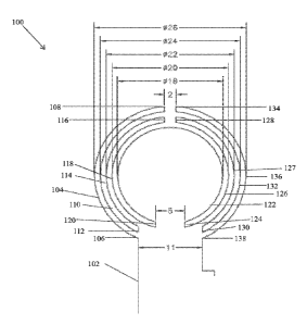
FIG. 1 illustrates a circular inlay design for a UHF RFID tag, in accordance
with an
embodiment of the present specification. In various embodiments, a wire 102
may be embedded
in a substrate such PVC, PETG, etc. to obtain an inlay for a UHF RFID tag. In
an embodiment,
wire 102 may be embedded in a PVC sheet having thickness ranging from 0.1 to
0.3 mm.
As shown in FIG. 1A wire 102 is looped in a first partial circle 104 starting
at a first
proximal end 106 to a first distal end 108 and then turned into in a second
partial circle 110
starting from the first distal end 108 to a second proximal end 112 which is
separated from the
first proximal end 106 by a distance of approximately 2mm. Wire 102 is next
looped into a third
partial circle 114 starting from the second proximal end 112 to a second
distal end 116 and then
into a fourth partial circle 118staring from the second distal end 116 to a
third proximal end 120,
wherein the third proximal end is separated from the second proximal end by a
distance of
approximately 2mm and the second distal end is separated from the first distal
end by a distance
of approximately 2mm.
Wire 102 is next looped into a circular loop 122 all the way from the third
proximal end
120 to a fourth proximal end 124. In an embodiment, the distance separating
the third proximal
120 end and the fourth proximal end 124 is approximately 5 mm as shown in the
figure; and the
diameter of the circular loop 122 is approximately 18 mm. Wire 102 is next
looped into a fifth
5
CA 02991561 2018-01-05
WO 2017/006350
PCT/1N2016/050223
partial circle 126 starting from the fourth proximal end 124 to a third distal
end 128, wherein the
third distal end 128 is separated from the second distal end by a distance of
approximately 2mm.
Wire 102 is next looped into a sixth partial circle 127 starting from the
third distal end 128 to a
fifth proximal end 130, wherein the fifth proximal end 130 is separated from
the fourth proximal
end 124 by a distance of approximately 2 mm. Wire 102 is next looped into a
seventh partial
circle 132 starting from the fifth proximal end 130 to a fourth distal end
134; and then into an
eighth partial circle 136 starting from the fourth distal end 134 to a sixth
proximal end 138,
wherein the fourth distal end 134 is separated from the third distal end 128
by a distance of
approximately 2 mm ; and the fifth proximal end 130 is separated from the
sixth proximal end
138 by a distance of approximately 2 mm.
In an embodiment, the sixth proximal end 138 is separated from the first
proximal end
106 by a distance of approximately 11 mm. Further, the distance between the
first and fourth
distal ends and second and third distal ends respectively is approximately 2
mm. Also, in an
embodiment, the diameter of a partial circle formed by the fourth loop 118 and
the fifth loop 126
is approximately 20 mm; the diameter of a partial circle formed by the third
loop 114 and the
sixth loop 127 is approximately 22 mm; the diameter of a partial circle formed
by the second
loop 110 and the seventh loop 132 is approximately 24 mm; and the diameter of
a partial circle
formed by the first loop 104 and the eight loop 136 is approximately 26 mm.
FIG. 1B illustrates a UHF transponder/chip fitted in a gap in the circular
loop structure of
wire, in accordance with an embodiment of the present specification. In
various embodiments a
UHF transponder/chip 150 is fitted in the gap 152 between the third proximal
end 120 and the
fourth proximal end 124 and is coupled with the wire 102. In an embodiment, an
EPC Class 1
Generation 2 chip 840 MHz ¨ 960 MHz frequency range is fitted in the gap 152
coupled with
wire 102.
FIG. 1C illustrates substrate specifications for an inlay design of a UHF RFID
tag, in
accordance with an embodiment of the present specification. In an embodiment,
thickness of the
substrate 130 ranges from 0.10 to 0.30 mm. In an embodiment, an inner diameter
136 of inlay
design 100 measures 15.90 mm, while an outer diameter 138 measures 27 mm, as
shown in FIG.
6
CA 02991561 2018-01-05
WO 2017/006350
PCT/1N2016/050223
1C. Also, in an embodiment, the total length of wire used in the inlay design
100 is
approximately 300.5 mm.
In an embodiment, the wire inlay design as shown in FIG. 1A has an outer
diameter of 27
mm and an inner punch of 16 mm and is extracted from the substrate which
results in the inlay
having the structure of a ring. The inlay is thereafter pasted with a
polyester grade circular ring
from one side to protect the inlay ring. Next, the inlay ring along with the
protective coating is
treated with an outer and an inner punch. This gives the UHF inlay with wire
embedding strength,
and is thereafter placed into plastic for use as animal ear tag.
FIG. 2 illustrates the stages of employing a UHF wire inlay into an RFID tag.
The UHF
inlay is in the form of a circular ring 202 after being extracted from the
substrate. Circular inlay
202 is bonded with a protective ring 204, covering the looped wire and the
transponder chip. In
an embodiment, the protective ring is made of a flexible polymer based
material such as but not
limited to polyester, vinyl and Polypropylene (PP). Next, the protective ring
204 is bonded with a
ring 206 made of any filler material such as but not limited to Epoxy (1 part
or 2 part), or any
adhesive filling material to further strengthen the wire inlay 202. Next, the
strengthened ring
structure is placed within a tag made of a plastic material. The tag comprises
two halves ¨ a
cover portion 208 and a base portion 210 made of a thermoplastic material. The
strengthened
inlay ring is placed between the cover 208 and the base 210 and then the two
halves are sealed
together to form a UHF RFID tag which may be pinned on an animal ear or put to
any other
suitable use.
It is submitted that the length, the gap in between and the number of turns of
the wire in
the tag may vary depending upon the needs to tune the desired frequency.
Accordingly, the
above examples are merely illustrative of the many applications of the system
of present
invention. Although only a few embodiments of the present invention have been
described herein,
it should be understood that the present invention might be embodied in many
other specific
forms without departing from the spirit or scope of the invention. Therefore,
the present
examples and embodiments are to be considered as illustrative and not
restrictive, and the
invention may be modified within the scope of the appended claims.
7