Note: Descriptions are shown in the official language in which they were submitted.
Aperture Multiplier Using a Rectangular Waveguide
FIELD AND BACKGROUND OF THE INVENTION
The present invention relates to optical aperture multipliers and, in
particular, it concerns
an optical aperture multiplier that includes a rectangular waveguide, and near-
eye displays and
head-up displays which employ such aperture multipliers.
Optical arrangements for near eye display or head up display require large
aperture to
cover the area where the observer's eye is located (the eye motion box). In
order to implement a
compact device, the image is generated by small optical image generator having
small aperture
that is multiplied to generate a large aperture.
An approach to aperture multiplication in one dimension has been developed
based on a
parallel-faced slab of transparent material within which the image propagates
by internal
reflection. Part of the image wavefront is coupled out of the slab, either by
use of obliquely
angled partial reflectors or by use of a diffractive optical element on one
surface of the slab. Such
a slab is referred to herein as a one-dimensional waveguide in that it
contains the image
wavefront by internal reflection in one dimension. In the plane of the slab
(i.e., of the slab
surfaces), the image must be collimated so as to maintain image quality across
the waveguide.
The slab-propagation approach is quite suitable for a second stage of aperture
multiplication, where the slab is deployed opposite the eye of the observer
(like a glasses lens for
near-eye displays, or a window for larger head-up displays) and forms the
final output surface
from which the image reaches the eye. This approach is however non-optimal for
a first stage of
multiplication, where the requirements for width of the slab compared to the
width of the image
wavefront add bulk and weight to the device.
SUMMARY OF THE INVENTION
The present invention is an optical aperture multiplier that includes a
rectangular
waveguide.
According to the teachings of an embodiment of the present invention there is
provided,
an optical aperture multiplier comprising: (a) a first optical waveguide
having a direction of
elongation, the first optical waveguide having first and second pairs of
parallel faces forming a
rectangular cross-section, wherein a plurality of partially reflecting
surfaces at least partially
traverse the first optical waveguide, the partially reflecting surfaces being
at an oblique angle to
the direction of elongation; and (b) a second optical waveguide optically
coupled with the first
optical waveguide, the second optical waveguide having a third pair of
parallel faces forming a
CA 2992213 2018-02-20
slab-type waveguide, wherein a plurality of partially reflecting surfaces at
least partially traverse
the second optical waveguide, the partially reflecting surfaces being at an
oblique angle to the
third pair of parallel faces, wherein the optical coupling and the partially
reflecting surfaces of
the first and second waveguides are configured such that, when an image is
coupled into the first
optical waveguide with an initial direction of propagation at a coupling angle
oblique to both the
first and second pairs of parallel faces, the image advances by four-fold
internal reflection along
the first optical waveguide, with a proportion of intensity of the image
reflected at the partially
reflecting surfaces so as to be coupled into the second optical waveguide, and
propagating
through two-fold reflection within the second optical waveguide, with a
proportion of intensity
of the image reflected at the partially reflecting surfaces so as to be
directed outwards from one
of the parallel faces as a visible image.
According to a further feature of an embodiment of the present invention, the
first pair of
parallel faces comprises a first face and a second face, and the second pair
of parallel faces
comprises a third face and a fourth face, an end of the first face terminating
at a first proximal
edge and an end of the third face terminating at a second proximal edge, the
optical aperture
multiplier further comprising a coupling reflector arrangement integrally
formed, or optically
coupled, with the optical waveguide, the coupling reflector arrangement
comprising: (a) a first
reflector deployed as a proximal extension of the third face, or as a
reflector parallel and external
to the third face, the first reflector having a width perpendicular to the
direction of elongation
that is greater than a width of the third surface, and (b) a second reflector
deployed as a proximal
extension of the fourth face, or as a reflector parallel and external to the
fourth face, the second
reflector having a width perpendicular to the direction of elongation that is
greater than a width
of the fourth surface, such that, when viewed along an optical input axis, the
first and second
proximal edges present an apparent waveguide aperture bounded by the first and
second
proximal edges and images of the first and second proximal edges reflected in
the coupling
reflector arrangement.
According to a further feature of an embodiment of the present invention, the
optical
input axis is oblique to both the first and second reflectors.
According to a further feature of an embodiment of the present invention, the
coupling
reflector arrangement is implemented as a coupling prism integrally formed, or
optically
coupled, with the optical waveguide, the coupling prism presenting a coupling
surface generally
perpendicular to the optical input axis.
According to a further feature of an embodiment of the present invention, the
coupling
reflector arrangement is implemented as a coupling prism integrally formed, or
optically
2
CA 2992213 2018-02-20
coupled, with the optical waveguide, the coupling prism being integrated with
at least one optical
element of an image projection arrangement.
According to a further feature of an embodiment of the present invention, the
at least one
optical element comprises a beam splitter prism having an input face, a
reflector face, an internal
inclined beam-splitting element and an output face generally orthogonal to a
primary direction of
output image propagation, and wherein at least part of the first and second
reflectors of the
coupling reflector extend across a plane of the output face.
According to a further feature of an embodiment of the present invention, the
coupling
reflector arrangement is implemented as a coupling prism integrally formed, or
optically
coupled, with the optical waveguide, the coupling prism presenting an oblique
reflecting surface
for reflecting light input along an optical axis perpendicular to one of the
first and second
reflectors so as to impinge on the apparent waveguide aperture.
According to a further feature of an embodiment of the present invention,
there is also
provided an image projector deployed to project an image collimated to
infinity along the optical
input axis so as to fully overlap the apparent waveguide aperture.
According to a further feature of an embodiment of the present invention,
there is also
provided a depolarizer element interposed in an optical path between the image
projector and the
coupling reflector arrangement.
According to a further feature of an embodiment of the present invention, the
first optical
waveguide is optically coupled to an end surface of the second optical
waveguide, the end
surface extending between the third pair of parallel faces.
According to a further feature of an embodiment of the present invention, the
end surface
is orthogonal to the third pair of parallel faces. According to an alternative
feature of an
embodiment of the present invention, the end surface is angled obliquely to
the third pair of
parallel faces.
According to a further feature of an embodiment of the present invention, the
partially
reflective surfaces of the second waveguide intersect a first of the third
pair of parallel faces at a
set of parallel lines, and wherein the end surface meets the first of the
third pair of parallel faces
along an edge, the edge being non-parallel to the set of parallel lines.
According to a further feature of an embodiment of the present invention, the
first optical
waveguide is optically coupled to one of the third pair of parallel faces.
According to a further feature of an embodiment of the present invention, the
partially
reflecting surfaces of the first waveguide are at an oblique angle to both the
first pair of parallel
faces and the second pair of parallel faces.
3
CA 2992213 2018-02-20
According to a further feature of an embodiment of the present invention, at
least one
face from the first and second pairs of parallel faces is coated with layers
of a dielectric material
to form a dielectric mirror.
According to a further feature of an embodiment of the present invention, one
of the faces
of the first optical waveguide is a coupling face through which the first
optical waveguide is
optically coupled with the second optical waveguide, and wherein the plurality
of partially
reflecting surfaces of the first waveguide are in overlapping relation such
that, in a geometrical
projection of the partially reflecting surfaces along a primary image
propagation direction onto
the coupling face, a majority of an area lying within the projection is
included within projections
of at least two of the partially reflecting surfaces.
According to a further feature of an embodiment of the present invention,
there is also
provided an image projecting arrangement associated with the first waveguide
and deployed to
introduce into the first waveguide a first image with a first spread of
angular directions, and
wherein the four-fold internal reflection generates second, third and fourth
conjugate images
having respective second, third and fourth spreads of angular directions, the
plurality of partially
reflecting surfaces of the first optical waveguide being coated so as to
render them substantially
transparent to rays of the image incident within a first range of angles to
the partially reflecting
surfaces and partially reflecting to rays of the image incident within a
second range of angles,
wherein the first spread of angular directions and the oblique angle of the
plurality of partially
reflecting surfaces are chosen such that the spread of angular directions for
three of the four
conjugate images are all incident on the plurality of partially reflecting
surfaces within the first
range of angles and the spread of angular directions for only one of the four
conjugate images is
incident on the plurality of partially reflecting surfaces within the second
range of angles.
There is also provided according to the teachings of an embodiment of the
present
invention, an optical aperture multiplier comprising: (a) an optical waveguide
having a direction
of elongation, the optical waveguide having a first pair of parallel faces
comprising a first face
and a second face, and a second pair of parallel faces comprising a third face
and a fourth face,
the pairs of parallel faces together forming a rectangular cross-section, an
end of the first face
terminating at a first proximal edge and an end of the third face terminating
at a second proximal
edge; and (b) a coupling reflector arrangement integrally formed, or optically
coupled, with the
optical waveguide, the coupling reflector arrangement comprising: (i) a first
reflector deployed
as a proximal extension of the third face, or as a reflector parallel and
external to the third face,
the first reflector having a width perpendicular to the direction of
elongation that is greater than a
width of the third surface, and (ii) a second reflector deployed as a proximal
extension of the
4
CA 2992213 2018-02-20
fourth face, or as a reflector parallel and external to the fourth face, the
second reflector having a
width perpendicular to the direction of elongation that is greater than a
width of the fourth
surface, such that, when viewed along an optical input axis, the first and
second proximal edges
present an apparent waveguide aperture bounded by the first and second
proximal edges and
images of the first and second proximal edges reflected in the coupling
reflector arrangement.
According to a further feature of an embodiment of the present invention, the
optical
input axis is oblique to both the first and second reflectors.
According to a further feature of an embodiment of the present invention, the
coupling
reflector arrangement is implemented as a coupling prism integrally formed, or
optically
coupled, with the optical waveguide, the coupling prism presenting a coupling
surface generally
perpendicular to the optical input axis.
According to a further feature of an embodiment of the present invention,
there is also
provided an image projector deployed to project an image collimated to
infinity along the optical
input axis so as to fully overlap the apparent waveguide aperture.
According to a further feature of an embodiment of the present invention,
further
comprising a depolarizer element interposed in an optical path between the
image projector and
the coupling reflector arrangement.
There is also provided according to the teachings of an embodiment of the
present
invention, an optical aperture multiplier comprising: (a) a first optical
waveguide having a
direction of elongation, the first optical waveguide having first and second
pairs of parallel faces
forming a rectangular cross-section, wherein a plurality of partially
reflecting surfaces at least
partially traverse the first optical waveguide, the partially reflecting
surfaces being at an oblique
angle to the direction of elongation, the plurality of partially reflecting
surfaces of the first
optical waveguide being coated so as to render them substantially transparent
to rays incident
within a first range of angles to the partially reflecting surfaces and
partially reflecting to rays
incident within a second range of angles; and (b) an image projecting
arrangement associated
with the first waveguide and deployed to introduce into the first waveguide a
first image with a
first spread of angular directions, wherein the first image advances by four-
fold internal
reflection along the first optical waveguide, thereby generating second, third
and fourth
conjugate images having respective second, third and fourth spreads of angular
directions, and
wherein the first spread of angular directions and the oblique angle of the
plurality of partially
reflecting surfaces are chosen such that the spread of angular directions for
three of the four
conjugate images are all incident on the plurality of partially reflecting
surfaces within the first
5
CA 2992213 2018-02-20
range of angles and the spread of angular directions for only one of the four
conjugate images is
incident on the plurality of partially reflecting surfaces within the second
range of angles.
BRIEF DESCRIPTION OF THE DRAWINGS
The invention is herein described, by way of example only, with reference to
the
accompanying drawings, wherein:
FIGS. IA and I B are schematic side and front representations, respectively,
of an optical
aperture multiplier, constructed and operative according to the teachings of
an embodiment of
the present invention;
FIGS. 2A and 2B are schematic diagrams illustrating two possible geometries of
image
rays propagating relative to partially reflecting internal facets in
waveguides from the optical
aperture multiplier of FIGS. IA and 1B;
FIG. 3 is a schematic two-dimensional projection of angular relationships
between the
various reflected images and internal facets of the optical aperture
multiplier of FIGS. IA and
1B;
FIGS. 4A-4D are schematic isometric representations showing the
interrelationship
between various conjugate images and their reflections in internal facets for
the optical aperture
multiplier of FIGS. IA and 1B;
FIGS. 5A-5D are schematic representations of the relationships between various
rays in
conjugate images propagating along a 2D waveguide from the optical aperture
multiplier of
FIGS. IA and 1B, for various initial ray directions and various geometrical
forms of waveguide;
FIG. 6 is a schematic isometric view of a coupling reflector arrangement for
coupling-in
an image to a 2D waveguide from the optical aperture multiplier of FIGS. IA
and 1B according
to a further aspect of the present invention;
FIG. 7 is a variant implementation of the coupling reflector arrangement of
FIG. 6;
FIGS. 8A and 8B are isometric views from different viewpoints of a waveguide
and
coupling reflector arrangement equivalent to FIG. 6 in which the coupling
reflector arrangement
is implemented as part of a coupling prism;
FIGS. 9A and 9B are views similar to FIGS. 8A and 8B, respectively, showing a
variant
implementation of the coupling prism;
FIGS. 10A-10C are an isometric view, top view and side view, respectively, of
an
alternative implementation of a coupling prism and 2D waveguide;
FIGS. 11, 12 and 13A are isometric views of three further variant
implantations of the
coupling prism and 2D waveguide of FIG. 10A;
6
CA 2992213 2018-02-20
FIG. I3B is a top view of the coupling prism and 2D waveguide of FIG. 13A;
FIGS. 14A-14C arc schematic isometric views of three stages during the
production of
the coupling prism and 2D waveguide of FIG. 10A according to a further aspect
of the present
invention;
FIG. 15 is a schematic side view illustrating integration of an image
projecting
arrangement with a 2D waveguide according to a further aspect of the present
invention;
FIGS. 16 and 17 are schematic side views illustrating two variant
implementations of the
integrated image projecting arrangement and 2D waveguide of FIG. 15;
FIG. 18 is an isometric view of an exemplary implementation of the principles
of FIGS.
15-17 in three dimensions;
FIGS. 19A-19C are schematic isometric, side and top views, respectively,
illustrating a
variant coupling geometry between a 2D waveguide and a I D waveguide according
to a further
implementation of the present invention;
FIG. 20 is a schematic isometric representation showing the interrelationship
between
various conjugate images and their reflections in internal facets for the
optical aperture multiplier
of FIGS. 19A-19C;
FIGS. 21A-21C are schematic side views illustrating thr:re variant
implementations of
coupling geometry between a 2D waveguide and a 1D waveguide according to
teachings of the
present invention;
FIGS. 22A and 22B are schematic isometric and side views, respectively,
illustrating a
further variant implementation of coupling a geometry between a 2D waveguide
at an oblique
angle to a ID waveguide according to an implementation of the present
invention;
FIGS. 22C-22E are schematic side views similar to FIG. 22B illustrating
various variant
implementations;
FIG. 23 is a schematic side view of an optical aperture multiplier similar to
that of FIG.
IA, but employing a refractive layer interposed between two waveguides;
FIG. 24 is a representation similar to FIG. 3 illustrating the relevant
angular relationships
for the device of FIG. 23;
FIGS. 25A-25C are side views of a device similar to that of FIG. IA
illustrating various
implementation options for mechanical interconnection of the two waveguides;
FIG. 25D is a side view of a device similar to that of FIG. 22E illustrating
an
implementation option for mechanical interconnection of the two waveguides;
7
CA 2992213 2018-02-20
FIG. 26 is a front view of a device similar to that of FIG. 1B illustrating a
relative
inclination between the first waveguide and a direction of image propagation
in the second
waveguide;
FIG. 27 is a schematic isometric view illustrating an implementation of a 2D
waveguide
with internal partially reflective facets inclined obliquely relative to
relative to both sets of
elongated parallel external faces;
FIGS. 28 and 29A are representations similar to FIG. 3 illustrating the
geometrical
angular relationships for two exemplary implementations of a device employing
the 2D
waveguide of FIG. 27 with first and second internal facet orientations,
respectively;
FIG. 29B is a schematic isometric representation of angles of image
propagation within
the 2D waveguide according to the implementation of FIG. 29A;
FIG. 30 is a schematic front view of a waveguide according to a further aspect
of the
present invention juxtaposed with an adjacent waveguide to provide uniformity
enhancement;
FIGS. 31A and 31B are schematic views of a waveguide illustrating the effects
of
variation in internal facet spacing on image uniformity according to a further
aspect of the
present invention;
FIG. 31C is a front view of a system similar to that of FIG. 1B illustrating a
multi-path
implementation for enhancing image uniformity;
FIGS. 32A and 32B are two further variant multi-path implementations of a
system
similar to that of FIG. 1B;
FIG. 33A is a schematic front view of a further alternative implementation of
a device
similar to FIG. 1B employing internal facets coated so as to selectively
reflect shallow angle of
incidence rays;
FIG. 33B is a representation similar to FIG. 3 illustrating angular
relationships between
the various reflected images and internal facets of the optical aperture
multiplier of FIG. 33A;
FIG. 33C is a graph illustrating the angular dependence of reflectivity for S
and P
polarized radiation for coated facets used in the device of FIG. 33A;
FIGS. 34A-34E are schematic isometric views illustrating a sequence of steps
in
production of a 2D waveguide and coupling prism according to an aspect of the
present
invention;
FIGS. 35A and 35B are schematic front and side views, respectively,
illustrating the
potential impact of an embodiment of the present invention on intensity of a
transmitted view of
a directly viewed scene; and
8
CA 2992213 2018-02-20
FIGS. 35C and 35D arc views similar to FIGS. 35A and 35B illustrating a
transmitted
view intensity correction according to a further aspect of the present
invention.
DESCRIPTION OF THE PREFERRED EMBODIMENTS
The present invention is an optical aperture multiplier that includes a
rectangular
waveguide.
The principles and operation of optical aperture multipliers according to the
present
invention may be better understood with reference to the drawings and the
accompanying
description.
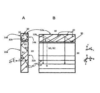
Referring now to the drawings, FIGS. 1A-35 illustrate various aspects of an
optical
aperture multiplier, constructed and operative according to certain
embodiments of the present
invention. In general terms, an optical aperture multiplier according to an
embodiment of the
present invention includes a first optical waveguide 10 having a direction of
elongation
illustrated arbitrarily herein as corresponding to the "x-axis". First optical
waveguide 10 has first
and second pairs of parallel faces 12a, 12b, 14a, 14h forming a rectangular
cross-section.
According to certain particularly preferred embodiments of the present
invention, a plurality of
internal partially reflecting surfaces 40, referred to herein as "facets", at
least partially traverse
first optical waveguide 10 at an oblique angle (i.e., neither parallel nor
perpendicular) to the
direction of elongation.
The optical aperture multiplier preferably also includes a second optical
waveguide 20,
optically coupled with first optical waveguide 10, having a third pair of
parallel faces 22a, 22h
forming a slab-type waveguide, i.e., where the other two dimensions of
waveguide 20 are at least
an order of magnitude greater than the distance between third pair of parallel
faces 22a, 22b.
Here too, a plurality of partially reflecting surfaces 45 preferably at least
partially traverse
second optical waveguide 20 at an oblique angle to the third pair of parallel
faces.
The optical coupling between the waveguides, and the deployment and
configuration of
partially reflecting surfaces 40, 45 are such that, when an image is coupled
into first optical
waveguide 10 with an initial direction 30 of propagation at a coupling angle
oblique to both the
first and second pairs of parallel faces 12a, 12b, 14a, 14b, the image
advances by four-fold
internal reflection (images al, a2, a3 and a4) along first optical waveguide
10, with a proportion
of intensity of the image reflected at partially reflecting surfaces 40 so as
to be coupled into
second optical waveguide 20, and then propagates through two-fold reflection
(images hi, b2)
within second optical waveguide 20, with a proportion of intensity of the
image reflected at
9
CA 2992213 2018-02-20
partially reflecting surfaces 45 so as to be directed outwards from one of the
parallel faces as a
visible image c, seen by the eye of a user 47.
Turning now more specifically to FIGS. IA and 1B, this shows a first
illustration of an
implementation of the above description. First waveguide 10 is referred to
herein as a 2D
waveguide in the sense that it guides the injected image in two dimensions by
reflection between
two sets of parallel faces, while second waveguide 20 is referred to as a ID
waveguide, guiding
the injected image in only one dimension between one pair of parallel faces.
Light beam 30 from
an optical image generator (not depicted) is injected into first waveguide 10
at an angle.
Consequently, the light propagates along waveguide 10 while being reflected
from all four
external faces of the waveguide as shown in the side view of FIG. IA. In this
process, four
conjugate beam vectors are generated at, a2, a3 and a4 which represent the
same image as it is
reflected internally by the faces.
The angle of beam 30 that is injected into waveguide 10 is set to reflect from
all four
external faces of this waveguide. The light beam should reflect from the
bottom face 12h of first
waveguide 10, i.e., the face adjacent to second waveguide 20, at shallow
(grazing) angles and
should transmit from 10 into 20 at steep angles. This property can be achieved
by total internal
reflection (TIR) or by optical ,:,oating. A diffractive pattern can also
perform this optical property
by combining diffraction with transmission on the same surface. Reflection
from the other three
faces 12a, 14a and 14b of first waveguide 10 can be generated the same way or
by use 01 a
reflecting coating.
Part of the guided light-beams (for example al and a2) within first waveguide
10 are
reflected by the internal parallel partial reflectors (facets) 40 downward
onto an input coupling
surface of second waveguide 20. In second waveguide 20, these beams are
defined as bl and b2.
Beams bl and b2 are reflected by the external faces and become conjugate,
i.e., beam bl
is reflected to be b2 and vice versa (as depicted in FIG. IA). The external
front and back faces
14a, 14h of first waveguide 10 should be parallel to each other and, in this
implementation, to
the corresponding external faces 22a, 22b of second waveguide 20. Any
deviation from
parallelism will cause the coupled images bl and b2 not to be precise
conjugate images, and
image quality will degrade.
The internal facets 45 within second waveguide 20 reflect beam b2 outside the
wavegu ides and into the eye of the observer 47.
The reflection process by the internal facets in waveguides 10 and 20 is
further explained
in FIGS. 2A and 28. Two basic configurations are depicted, and differ by the
relative angles of
the light beams and the facets. In this schematic illustration, the beams al,
a2 and bl are
CA 2992213 2018-02-20
depicted as same vector (reference will be only to 14) since the same
geometrical considerations
apply to each as observed from a side view of the corresponding waveguide.
Beams a3, a4 and
b2 are also depicted as same vector (reference will be only to b2).
Light beams b2 are actually a bundle of rays propagating in same direction as
depicted by
two vectors in FIG. 2A. In this case, one vector is reflected by the external
face to become bl
and onto the internal facet 40 (or 45) where part of it is reflected as cl.
The other b2 vector is
reflected directly by facet as vector c2. The vectors cl and c2 represent the
normal image and
ghost image not necessarily in this order. In this configuration, bl and b2
impinge on facet 45
from the same side.
Parenthetically, wherever an image is represented herein by a light beam, it
should be
noted that the beam is a sample beam of the image, which typically is formed
by multiple beams
at slightly differing angles each corresponding to a point or pixel of the
image. Except where
specifically referred to as an extremity of the image, the beams illustrated
are typically a centroid
of the image.
FIG. 2B describes essentially the same process but where the geometry is such
that bl
and b2 impinge on facet 40 (or 45) from opposite sides.
In both case:., the magnitude of reflection for images el and c2 in S and P
polarizations is
determined by the coating on these facets. Preferably one reflection is the
image and the other is
suppressed since it corresponds to an unwanted "ghost" image. Suitable
coatings for controlling
which ranges of incident beam angles are reflected and which ranges of
incident beam angles are
transmitted are known in the art, and can be found described in detail in US
Patents Nos.
7391573 and 7457040, coassigned with the present invention.
It is particularly preferred to design the system so that "ghost" images do
not overlap the
main or the conjugate images (el overlapping c2). The process of designing the
appropriate
angle of the beams while maintaining T1R conditions for propagation of the
images within the
waveguides, and at the same time avoiding ghost-overlap, is described in FIG.
3. This drawings
introduces a schematic representation which will be used further below to
present additional
embodiments of this invention.
Thus FIG. 3 shows a projection of the geometry of waveguides 10 and 20 in
which
rotations are depicted as distance along the rectilinear axes ("angular
space"). The diagram thus
represents spherical coordinates in Cartesian coordinates. This representation
introduces various
distortions, and displacements along the different axes are non-commutative
(as is the nature of
rotations about different axes). Nevertheless, this form of diagram has been
found to simplify the
11
CA 2992213 2018-02-20
description and provide a useful tool for system design. For clarification,
the directions along X,
Y and Z axes are marked, according to one sequence of rotations.
The large circles represent the critical angle (boundary of Total Internal
Reflection - TIR)
of various external faces of the waveguides. Thus, a point outside a circle
represents an angular
direction of a beam that will be reflected by T1R, while a point inside a
circle represents a beam
that will pass the face and transmit out of the waveguide. The circles 57 and
59 represent the
critical angle of front and back external faces 14a and 14b of waveguide 10
and 220 and 226 of
waveguide 20. The "distance" between the circles of opposite facets is 180
degrees. The circles
61 and 63 represent the critical angle of the top and bottom external faces
12a and 12b of
waveguide 10. The dotted-dashed lines 65 and 67 represent the orientation of
these external faces
of the waveguides.
As previously described, the image is injected into the 2D waveguide 10 while
experiencing internal reflection. In the following example, all reflections
are TIR based,
therefore the injected image al is shown in FIG. 3 to be outside any circle. A
square image in the
angular space has a square shape.
As the image ails reflected from the external faces 12a, 12b, 14a and 14b of
waveguide
10 (rep: esented by orientations 65 and 67), it is multiplied to a2, a3, a4
and back to al
(represented schematically by four curved solid arrows). The reflection of
every image has the
same angular "distance" from each of faces (lines 65 and 67) as the image
itself, but on the other
side, according to the optical principle that the angle of reflection equals
the angle of incidence.
The orientation of internal facets 40 (in FIG. 1B) is depicted here as a line
70 that is
located according to the facets' angular inclination. As images al or a2
encounter the facet 70
(40) they are reflected to an equal opposite angular distance from 70 as
depicted by the dashed
arrow lines onto images bl and b2, respectively.
Since bl and b2 are within the critical angle boundary 61 of the bottom
external face of
First waveguide 10, they will be coupled out of this waveguide and into second
waveguide 20.
As images bl and b2 propagate within waveguide 20 they are mutually exchanged
by
reflection from front and back external faces 22a and 22b which have angular
orientation 67 (the
reflection being depicted as a curved solid double headed arrow).
Finally, image bl encounters internal facets 45 (FIG. 1A) at orientation 72
and are
reflected into image c. Since image c is within the critical angle circle 57,
it is coupled out of the
second waveguide 20 and onto the eye (47 in FIG. IA).
12
CA 2992213 2018-02-20
In all this configuration, the angle of the internal facets (70 and 72) must
not cross the
angular shape (square) of any of the images, since crossing like this will
cause "ghost" image to
overlap a normal image.
Image e can be designed to emerge at an arbitrary angle relative to waveguide
20 (not
necessarily perpendicular), as exemplified in FIG. 3, where c is not centered
on direction Z.
Facets 40 and 45 preferably are provided with coatings, as mentioned above,
which
reduce or substantially eliminate reflection of the low-angle images a3, a4
and b2, respectively.
The calculation process described in FIG. 3 was shown schematically in 2D
Cartesian
coordinates for ease and clarity of representation. Final accurate design of
the system is
performed in spherical coordinates, as illustrated in FIGS. 4A-4D. FIG. 4A
represents the
coupling between images al-a4. FIG. 4B shows the coupling al to bl and a2 to
b2 by reflection
on facets 40. FIG. 4C represents the coupling between bl and b2 in second
waveguide 20. FIG.
4D represents the coupling from bl to c by reflection on facets 45.
During the internal reflections within waveguide 10, there can be any number
of
reflections in every dimension (y or z) per roundtrip as shown in FIGS. 5A-5D.
FIG. 5A depicts
one reflection per external face. In this condition bl is originated by al.
However, since the
various light beams of different image field have different angles, eventually
the orientation of
reflection can change as the beams propagate along the x axis of waveguide 10.
FIG. 5B depicts
a different orientation that can evolve resulting in b2 being generated by a2.
Therefore, in every
design the generation of both bl and b2 should be assumed. The aspect ratio of
the waveguide 10
can be designed to have more than one reflection per external facet as
depicted in FIG. 5C. For
different field angle the orientation of the reflections can change as shown
in FIG. 5D. In fact,
certain particularly preferred implementations of the present invention ensure
that waveguide 10
is volumetrically filled with all four conjugate images al -a4, such that both
images al and a2
will always be out-coupled to produce bl and b2, except where special
precautions are taken to
suppress one of the paths, as discussed further below.
The combined reflections by the external faces and internal facets of
waveguides 10 and
20 expand the original injected aperture in both x and y dimensions. Waveguide
10 expands the
aperture in the x dimension and waveguide 20 in the y dimension (axes being
labeled as in FIG.
1B). The aperture expansion of first waveguide 10 is preferably achieved by
filling the
waveguide with the image and then coupling the image out of the waveguide via
the facets in a
continuous manner along the length of the waveguide, all as detailed further
below.
13
CA 2992213 2018-02-20
Coupling-In Arrangements
In order to obtain uniform intensity across the expanded aperture, the
injected initial
aperture of the beam should be uniform and should "fill" the waveguide. The
term "fill" is used
in this context to indicate that rays corresponding to each point (pixel) in
the image are present
across the entire cross-section of the waveguide. Conceptually, this property
implies that, if
waveguide 10 were to be cut transversely at any point, and if an opaque sheet
with a pinhole was
then placed over the cut end, the pinhole could be placed anywhere across the
cross-section and
would result in a complete projected image. In fact, for the 2D waveguide 10,
this would result
in projection of four complete images al, a2, a3 and a4, of which a2 and a4
are inverted.
In order to ensure filling of the waveguide with the input image, a slightly
oversize input
image should be trimmed to size on entry into the waveguide. This ensures that
the multiplied
adjacent apertures will not overlap on one hand and will not have gaps on the
other. The
trimming is performed as the light beam is injected into the waveguide.
A number of configurations for achieving effective coupling-in of an image to
first
waveguide 10 are illustrated in FIGS. 6-I3B. Turning first to FIGS. 6 and 7,
these illustrate
schematically a free-space mirror-implementation of a coupling-in arrangement
for trimming an
input image so as to uniformly fill first waveguide 10. In this case, face 12a
terminates at a first
proximal edge 16a and face 14a terminates at a second proximal edge 16h. In
order to fill the
waveguide fully, it is a particularly preferred feature of certain embodiments
of the present
invention that the optical aperture multiplier includes a coupling reflector
arrangement integrally
formed, or optically coupled, with first waveguide 10. The coupling reflector
arrangement
includes a first reflector 18a, deployed as a proximal extension of face 12b
(FIG. 6), or as a
reflector parallel and external to face 12b (FIG. 7), having a width
perpendicular to the direction
of elongation that is greater than a width of surface 12b. The coupling
reflector arrangement also
includes a second reflector 18b deployed as a proximal extension of face 14b
(FIG. 6), or as a
reflector parallel and external to face 14b, having a width perpendicular to
the direction of
elongation that is greater than a width of surface 14b. As a result of this
coupling reflector
arrangement, when viewed along an optical input axis (the viewpoint of FIGS. 6
and 7) along
which an image is to be introduced, first and second proximal edges 16a and
16b present an
apparent waveguide aperture bounded by the first and second proximal edges and
images of the
first and second proximal edges reflected in the coupling reflector
arrangement, corresponding
overall to an apparent aperture which is four times (2x2) the physical
aperture. Where the
coupling reflectors lie externally to the faces of the waveguide, the apparent
aperture is made up
of three images of the physical aperture slightly spaced apart from the
physical aperture itself,
14
CA 2992213 2018-02-20
where each aperture is framed by all four edges of the physical aperture. This
results in slight
inefficiency due to image intensity falling on the "spaces" between the
apertures being lost, but
filling of the aperture is still achieved.
In one preferred geometry as illustrated here, the optical input axis is
oblique to both the
first and second reflectors 18a and 18b. As clearly seen in these drawings,
the requirement for
the reflectors to have dimensions greater than those of the waveguide is here
required in order to
ensure that no clipping of the image and incomplete filling of the waveguide
occurs. In this
manner, the waveguide is reliably filled with all four images across its
entire cross-section.
While the use of free-space mirrors may in some cases be feasible, it is
typically
advantageous to implement the coupling reflector arrangement as a coupling
prism integrally
formed, or optically coupled, with waveguide 10, where first and second
reflectors 18a and 18b
are provided by faces of the coupling prism 91. A further face of the coupling
prism preferably
presents a coupling surface generally perpendicular to the optical input axis,
through which the
image is introduced. Examples of such an arrangement are illustrated in FIGS.
8A-8B and 9A-
9B, where FIGS. 8A-8B are geometrically equivalent to FIG. 6 and FIGS. 9A-9B
are
geometrically equivalent to FIG. 7. In these cases, the proximal "edges" of
waveguide 10 are
edges defined by the intersection of coupling prism surfaces with the
waveguide surfaces. In this
case, the other adjacent surfaces are preferably outwardly angled such that
light falling outside
those proximal edges will be reflected (or transmitted) in directions that do
not enter the
waveguide. Optionally, absorbent material may be applied to those surfaces to
further prevent
stray radiation from reaching undesired locations.
A further example of a coupling-in geometry is illustrated in FIGS. 10A-10C,
and
explains in more detail the progression of a sample wavefront during coupling-
in of an image to
the waveguide. In this case, beam 30 is injected having arbitrary initial
aperture lateral dimension
81 as measured along the x-axis, as shown in FIG. 10B. The front end of this
aperture is trimmed
by first proximal edge 16a as the beam enters the waveguide. The beam aperture
that was
trimmed on one side during entrance is reflected by the opposite coupling
reflector 18a and/or its
continuation face 12b back to the front face 12a where its back side is
trimmed once more by the
same first proximal edge 16a. As the beam propagates along the waveguide, its
apertures (84 and
88) are now adjacent without overlapping or gaps, thereby filling the
waveguide.
According to a particularly preferred implementation of the present invention,
a second
dimension of the beam's aperture is trimmed simultaneously by second proximal
edge 16b. The
relative orientations of proximal edges 16a and 16b are not critical. For
example, while in FIGS.
10A-10C edge 16a is shown inclined to the longitudinal x-axis, an alternative
geometry shown in
CA 2992213 2018-02-20
FIG. 11 where proximal edges 16a and 16h are both perpendicular to the
longitudinal x-axis may
in some cases simplify manufacture. The two proximal edges 16a and 16b
preferably intersect at
a corner, but this is not necessary as long as the optics is sufficiently wide
that the trimming is
performed only by proximal edges 16a and 16b and their reflections. A non-
intersecting example
is illustrated in FIG. 12.
The trimming in the second dimension occurs in a manner equivalent to that
described
for the first dimension with reference to FIG. 10B. Thus in FIG. IOC, the
initial untrimmed
projected image aperture has an initial aperture vertical dimension 92 as
measured along the x-
axis. As it enters at an angle from section 91 into waveguide 10, its front is
trimmed by second
proximal edge 16b. After the beam 92 is reflected from the opposite external
face 14a and/or its
continuation, its back side is also trimmed by second proximal edge 166 to be
at appropriate size
94. Consequently, all reflected apertures along this dimension are now also
adjacent. The overall
result of this trimming in two dimensions is that waveguide 10 is essentially
filled with all four
images/conjugate images al-a4, thereby facilitating subsequent uninterrupted
expansion of the
aperture along two dimensions.
Stops 16a and 16b can be produced using an absorbing material or as refractive
material
(such a prism or coating). For example, in FIGS. 10-13, they were depicted as
a step shape at the
entrance to the waveguide that acts to disperse the access light.
Coupling prism 91 can be manufactured either integrally with waveguide 10 or
by
attaching two components by known techniques. Certain particularly
advantageous approaches
to attachment of these components will be described further below.
As pointed out above, the optical axis of the image coupled into waveguide 10
is inclined
obliquely to both sets of parallel faces. However, this does not necessarily
require oblique
orientation of an image projector, since the required angle of image
propagation may be achieved
by other optical components, such as for example, an additional reflection at
an oblique
reflecting surface 91a of coupling prism 91 deployed to reflect light input
along an optical axis
perpendicular to the x-axis so as to impinge on the apparent waveguide
aperture.
Such an option is illustrated in FIGS. 13A and I3B, where oblique reflecting
surface 91a
provides a back mirror. As depicted in FIG. 13B, the arbitrary (oversized)
aperture 81 enters the
waveguide to be reflected by reflecting surface 91a while being trimmed by
16a. After one
reflection 82, the back side of the aperture is trimmed 84 by the same edge
16a.
The extra light of 81 is trimmed by edge 16a using two mechanisms: at
entrance, the
extra light continue propagation and transmitted outside over the edge (to the
left of) edge 16a,
16
CA 2992213 2018-02-20
while after reflection 82 to 84, the back side of the wave front is to the
right of edge 16a
therefore being reflected once more by 91a to angles outside TIR or outside
the relevant Image.
Edge 16h continues to trim the perpendicular axis as before in the other
dimension.
Optionally, mirror 91a may be inclined about two axes so as to generate a
desired direction of
propagation of the image when the input image 30 is perpendicular to one face
of the waveguide.
Thus, in summary, coupling of the image/beam into waveguide 10 at a desired
angle can
be achieved using a prism, a mirror placed in front, behind or within the
waveguide, or other
known methods. All of these methods are practical as long as the double-stop
configuration
described is present.
In order to achieve uniform intensity across the extended aperture, it is
preferable that
trimming edges 16a and 16h should be clean edges with minimal deviations and
scattering.
Residues of glue or other perturbing elements can cause degradation in
uniformity. FIGS. I 4A-
14C illustrate an additional aspect of the present invention, applicable also
in other contexts
where optical elements are to be joined, which facilitates formation of a
clean trimming edge (or
in other applications, continuous outer surface). The relevant external faces
(12a and 14b) of
waveguide 10 are first coated by a reflective or protective coating 1610. The
edge of the
waveguide 10 is then polished according to the required trimming edge 1630
(16a and 16h) and
finally prism 1640 is attached. In this attachment, the other two faces (on
the rear side of the
view as illustrated) must be an accurate continuation of the external surfaces
of waveguide 10 to
provide the coupling reflectors as continuations of those faces. If these
faces are not continuous
(as in FIG. 9b), then the reflective coating 1610 should preferably cover the
opposite faces (12b
and 14a) as well. This approach is relevant also to systems with ID
waveguides. The angle of the
coupling surfaces may be any orientation.
It should be noted that the above technique, namely providing a protective
dielectric or
reflective coating prior to finishing of a surface for coupling two optical
components, addresses a
widespread problem beyond the specific application described herein.
Specifically, whenever
two components are to be joined so as to provide an optical path from one to
the other, the
components must be joined by suitable optical adhesive, typically index-
matched to the
components. In order to ensure optimal optical coupling, the entire interface
surface should be
fully covered with the adhesive. On the other hand, precisely because of the
desired optical
properties of the adhesive, any overspill of adhesive from the interface to an
external surface of
the component will typically compromise the optical properties of the
component. By
preemptively coating the adjacent surfaces with a protective coating,
preferably prior to
polishing of the interface surface, the impact of any overspill of adhesive
onto the external
17
CA 2992213 2018-02-20
surfaces can be reduced or eliminated. Where two components are to be coupled
so that certain
surfaces will be flush after coupling, such coating may advantageously be
provided on both
components prior to coupling. In certain applications, coating on only one
side, or a subset of the
faces, may be sufficient, for example, where any excess glue on certain
surfaces could be readily
removed after bonding by a further polishing step.
The above implementations of coupling-in arrangements are preferably used
together
with an image projector deployed to project an image collimated to infinity
along the optical
input axis so as to fully overlap the apparent waveguide aperture. Any
suitable type and
technology of image projector may be used, including various free-space image
projectors. In
certain cases, in order to provide a particularly compact and rugged
implementation, the image
projector may be mechanically integrated (i.e., integrally formed or rigidly
interconnected) with
a coupling prism. Various implementations of this type will now be described
with reference to
FIGS. 15-18.
Referring first to FIG. 15, this illustrates an adaptation of the compact
image projector of
PCT Patent Publication No. WO 2015/162611 for use in the context of a 2D
waveguide, here
numbered 503. It includes Illumination Polarizing Beam Splitter (PBS) 500, a
collimating PBS
501, a coupling prism 502 (equivalent to 91 in FIGS. 10A-10C) coupling into
waveguide 503.
In the following description, the polarization management components
(including wave
plates and polarizers) are omitted for clarity. The illumination light 505
enters the illumination
prism 500 and is reflected by internal surface 507 onto the image generator
509, such as a liquid
crystal on silicon (LCOS) display. Light 511 reflected from the display passes
into collimating
prism 501 where surface 513 reflects the light onto a surface 515 with optical
power to achieve
collimation of the light to form a projected image at infinity. The collimated
light passes in
through coupling prism 502 to waveguide 503.
Surface 515 has a width 517 that is chosen to be sufficient to provide all of
the input
image angles required to "fill" waveguide 10 with the entire field of view
(FOV) of the image,
from a highest angle image angle 518a to a lowest image angle 5186, and
including a lowest
light ray in the FOV designated 519. The required size of surface 515, in
turn, determines the
required size of prisms 501 and 500. More specifically, as described above
with reference to
FIGS. 6-10C, it is desired for the waveguide 10 to be filled with the image
and its conjugate
images, meaning that the entire range of beam angles encompassed by the image
should be
incident on the entire width of the physical aperture of the waveguide as well
as the image of that
aperture in the coupling reflectors. By tracing these rays backwards from the
waveguide aperture
through the collimating PBS 501, it is possible to determine the minimum
required width 517 of
18
CA 2992213 2018-02-20
the collimating PBS, and hence also of the illumination/image-generating PBS
500. Proximal
edge 523 (corresponding to edge 16a above) then performs trimming of the image
wavefront as
described above.
FIG. 15 illustrates only one dimension, but the axes of the waveguide are
tilted relative to
those of the PBS such that this same image trimming occurs in both dimensions,
as described
above.
According to a further aspect of the present invention, which may be used to
advantage
also for coupling in an image to an otherwise conventional ID waveguide, it is
possible to
incorporate part or all of coupling prism 502 into collimating prism 501,
thereby reducing the
size of the system. Put in alternative terms, part of collimating PBS 501
lying below/beyond
surface 513 may be cut away to provide the required coupling reflector
surfaces.
One example of this approach is illustrated here in FIG. 16. In this figure,
the light
propagates as in FIG. 15, and the same numbering is used. Here, the
collimating prism 526
differs from prism 501 in that it abuts proximal edge 523 and has a modified
bottom face 528
forming a continuation of the bottom surface of waveguide 503 to provide the
coupling reflector.
In this configuration, the distance between the optical face 515 and the
trimming edge 523 is
substantially siiorter than in the implementation of FIG. 15. By tracing rays
backwards from the
optical aperture and the apparent optical aperture across the entire desired
angular field of view,
it may be seen that the required dimensions of the face 515 (and consequently
of prism 526) are
reduced. This in turn enables reduction of the dimensions of image generating
PBS 500.
The examples of FIGS. 15-17 illustrate cross-sectional geometry suitable for
implementation with either a ID waveguide or a 2D waveguide. When coupling
into a 2D
waveguide, the prism 526 (and 500 adjacent thereto) are at a two dimensional
tilt angle relative
to waveguide 503 (as shown for the coupling-in face of coupling prism 91 in
FIGS. 10A-10C).
Therefore, the geometry shown in FIG. 16 is reproduced in the other axis (with
different angles).
A second face of prism 526 perpendicular to face 528 will also be a
continuation of a second
surface of waveguide 503 (waveguide 10 in the previous figures). A three-
dimensional
representation of such an assembly is illustrated in FIG. 18. In this case,
the orientations of the
image-generating element, the prisms and the waveguide may be at arbitrary
rotations relative to
each other, all according to the requirements of each specific design.
The configurations of prism 526 according to this compact implementation
preferably
satisfy the following conditions:
1) The light from the optical face 515 is reflected directly onto the
waveguide and not being
reflected by surface 513 (equivalent to the above description of FIG. 15).
19
CA 2992213 2018-02-20
2) The image of the trimming edge 523 (represented for the shallowest-angle
part of the
image by beam 521) must not be truncated, not by reflecting surface 513 and
not by
external faces of prism 526.
3) Surface 528 must be continuation of the waveguide surface.
4) For a two-dimensional waveguide, the above conditions should be satisfied
in both
dimensions of the waveguide.
FIG. 17 illustrates how these limitations may dictate the degree to which it
is possible to
incorporate coupling prism 502 into a collimating prism 531. In this example,
the coupling angle
into the waveguide is very shallow. As a result, the coupling prism (before
being incorporated)
would have been very large and so would be the collimating and illumination
prisms. In this
embodiment the coupling prism was incorporated into collimating prism 531 only
to the point
where the image of the trimming edge for the shallowest angle portion of the
image (represented
as 521) is not compromised by the external face of the prism 531. This point
533 becomes the
edge of the coupling prism. The dimension 517 of optical element 515 is then
dictated by the
steepest angle portion of the image which must reach edge 523 unobstructed.
Since collimating
prism 531 of this dimension would fall short of direct abutment with edge 523,
a small coupling
prism 535 is provided at the entrance to waveguide 503.
In each of the above options for coupling-in of images into waveguide 10, the
solutions
presented are considered to be advantageous for any out-coupling applications
such as the
partially-reflective facet coupling-out approach discussed above, slanted-face
coupling out (such
as disclosed in PCT patent publication no. WO 2017/141242 A2) or for
applications using
diffractive elements for coupling-out. Slanted-face and diffractive elements
used for coupling-
out a proportion of the radiation impinging internally on a surface of a
waveguide are known in
the art, and will not be described here in detail.
Coupling Between First and Second Waveguides
The coupling from first waveguide 10 into second waveguide 20 according to the
configuration of FIGS. IA and 1B requires precise alignment of the waveguides
in order to
maintain image quality without creating double images. Specifically, as best
illustrated in FIGS.
IA, 3 and 5D, two output images al and a2 of the images in first waveguide 10
are coupled into
second waveguide 20, and continue to interchange with each other as conjugate
images bl and
b2 propagating along waveguide 20. In order to achieve good quality, the
external faces of
waveguides 10 and 20 should be precisely parallel or perpendicular to each
other. According to
the embodiment of FIGS. IA and I B, waveguide 10 is placed on top of waveguide
20.
Parenthetically, wherever reference is made herein to directions such as up,
down, top, bottom
CA 2992213 2018-02-20
etc., these terms are used only for ease of presentation and refer to the
arbitrary orientations as
illustrated in the drawings. The final device may be deployed in any required
orientation.
Furthermore, there is no limitation on the relative orientation of the
coupling-in arrangement for
introducing an image to the first waveguide and the coupling-out arrangement
for coupling an
image from the first waveguide to the second.
FIGS. 19A-19C illustrate a different configuration according to an embodiment
of the
present invention for coupling the waveguides by placing first waveguide 10
adjacent to one of
the parallel faces of second waveguide 20, as best seen in FIG. 19A. The light
propagates in first
waveguide 10 from right to left as shown, as described above with reference to
FIG. 1A, and
encounters the internal facets of waveguide 10 (visible in the top view of
FIG. 19C) which are
here oriented to deflect the deflected image so as to couple the image into
the face of second
waveguide 20 through an intermediate refractive layer 99 (discussed further
below). The
coupling is at an angle chosen so that the light beam continues to reflect
within second
waveguide 20, preferably through TIP. (solid arrows in FIG. 19B). The
conjugate beam that
couples into second waveguide 20 in the conjugate direction (dashed arrow in
FIG. 1913)
propagates to the adjacent end of second waveguide 20 and is lost by outward
scattering.
In this implementation, filling of second waveguide 20 with the coupled-in
image from
first waveguide 10 is preferably achieved by choosing a width of first
waveguide 10 sufficient
such that a light beam 101 emerging at an angle from the far end (top as shown
in FIG. I 9B) of
waveguide 10 for the most shallow-angle region of the image will not overshoot
the other end
102 of first waveguide 10.
In order to implement the configuration of FIGS. 19A-19C, a number of
conditions must
be met. Firstly, in order to support propagation along first waveguide 10, the
light beam
introduced into waveguide 10 must be reflected by the interface with
refractive layer 99. After
reflection by the internal facets of waveguide 10, the light beams should be
coupled out through
refractive layer 99 into second waveguide 20, but should not escape from the
opposite external
face of waveguide 20. FIG. 20 depicts in spherical coordinates an approach for
implementing
this configuration so as to satisfy the above conditions.
Thus, in FIG. 20, the images 106LU, 106RU, 106LD and 106RD are equivalent to
al,
a2, a3 and a4 of FIG. 1A. The critical angle between the waveguide and air is
represented by
circles 107 and 108, which are equivalent to 61 and 63, respectively, in FIG.
3. The circle 109
represents the critical angle between waveguide 10 and intermediate refractive
layer 99 of FIGS.
19B and 19C. Since the ratio of refractive indices of the waveguide and
refractive layer 99 is
smaller than to air, the TIR circle is larger than at the air boundary. The
four conjugate images
21
CA 2992213 2018-02-20
propagating along first waveguide 10 are all outside both circles 107 and 109,
so that the images
propagate through TIR along the waveguide. As 106LU encounters the internal
facet of
waveguide 10 (process described as image c2 in FIG 2A), it is coupled onto
110LU (equivalent
to bl in FIG. IA) while 106RU is coupled to 110RU. The beams 110LU and 110RU
are within
the critical angle 109 but outside the critical angle 107. As a result, they
will effectively couple
out of waveguide 10 through layer 99 and into waveguide 20, but will not
couple out to the air
from the external faces of waveguide 20.
As 110LU and 110RU are reflected within second waveguide 20, they generate
their
corresponding conjugate images HOLD and HORD, respectively. These reflections
are
equivalent to b2 in FIG. 1A.
As mentioned above, in this implementation, 110RU and HORD are scattered out
as
described by the dashed arrows in FIG. 19B. Images HOLD are coupled-out to the
eye by the
internal facets of second waveguide 20 (as was illustrated above at 45 in FIG.
IA).
Variant implementations of this embodiment are illustrated in FIGS. 21A and
21B. In
FIG. 21A, beams 110RU and HORD (depicted as dashed arrows) are reflected to
overlap and
reinforce 110LU and HOLD (solid arrows). This combination is achieved by
introducing a
reflector 112 perpendicularly and at the end of second waveguide 20 as shown
in FIG. 21A. This
reflector may cause some part of images 110RU and 11ORD to be reflected back
and reenter first
waveguide 10 in the opposite direction. It may be desirable to provide
reflective coatings on the
two opposite external facets 114R and 114L of first waveguide 10 to contain
these beams after
being reflected by the internal facets.
FIG. 21B illustrates a configuration which combines first waveguide reflector
114R with
second waveguide reflector 112 as a single reflector 116 while maintaining
same functionality as
the configuration of FIG. 21A.
In 21C, waveguide 10 is also adjacent to waveguide 20, spaced by an
intermediate
dielectric or air-gap. The light coupled-out from waveguide 10 (solid arrows)
is reflected by a
back mirror 117 on waveguide 20 in a process similar to the process described
above with
reference to FIGS. 13A and 13B. The angle of mirror 117 is chosen to match the
transmitted
light from waveguide 10 to the required guided light angle in waveguide 20
(dotted line). In
some cases, mirror 117 extends beyond the edge of waveguide 10 (as shown in
FIG 21C),
depending on the coupling-out angles generated by the implementation of
waveguide 10 and the
image propagation angles used.
22
CA 2992213 2018-02-20
Different geometries of image coupling-out by internal facets (or diffractive
optical
elements) can be applied to the implementations of FIGS. 19A-21C such as, for
example, the
various geometries and appropriate coatings described above with reference to
FIGS. 2A and 213.
The implementations of FIGS. 19A-21 B (NOT 21C) are somewhat limited in the
available field of view by the geometrical requirements described with
reference to FIG. 20.
Nevertheless, for a range of applications, this option may be particularly
advantageous due to
considerations of simplicity of the design and ease of manufacture.
A further set of implementations of coupling between first waveguide 10 and
second
waveguide 20 is illustrated in FIGS. 22A-22E. In these implementations, the 2D
waveguide 10 is
inclined relative to the second waveguide 20 so that only one of the images
coupled-out from
waveguide 10 is contained and guided within waveguide 20, as shown in FIG.
22B. First
waveguide 10 may be mounted at a required inclination relative to ID waveguide
20 by use of an
intermediate transparent wedge 730. This inclination is chosen so as to couple
one image from
waveguide 10 (solid arrow, analogous to the solid arrow of FIG. 19B) and not
to couple the other
image from waveguide 10 (dashed arrow, analogous to the dashed arrow of FIG.
19B). The
uncoupled image is absorbed by external absorber, for example 736 or directed
in a direction
where it will not be visible to the observer. Alternatively, 736 can 1:µ,: a
1D retro-reflector that
reflects the light (dot-dash arrow) back into waveguide 10 in the opposite
direction and couples
into waveguide 20, equivalent to dashed arrow in FIGS. 21A-21B. According to
this option, a
reflecting coating 737 may be provided on at least one of the external facets
of 2D waveguide 10,
as shown in FIG. 22B. For clarity of presentation, the internal facets of the
waveguides have
been omitted from these drawings.
The inclination of waveguide 10 relative to waveguide 20 can be chosen
according to the
required angles of the waveguides and the images propagating between them, and
may employ a
transparent wedge coupling prism 730 to either decrease the inclination
relative to an inclined
coupling surface of second waveguide 20, as shown in FIG. 22C, to increase the
angle as shown
in FIG. 22D. In one particularly preferred implementation as illustrated in
FIG. 22E, the required
inclination angle of first waveguide 10 relative to second waveguide 20
matches the angle of the
second waveguide coupling surface, so that no intermediate coupling prism is
needed. In order to
implement this option, the output angle of the image coupled into second
waveguide 20 must be
matched to the required propagation angle within waveguide 20, and the extent
of the wedge
formed by inclined end surface 734 and the dimensions of waveguide 10 must be
such that
filling of second waveguide 20 with the image and its conjugate are achieved,
in a manner
analogous to that described above with reference to FIGS. 6-12 above.
23
CA 2992213 2018-02-20
In each case, an interface discontinuity is required on the output face of
first waveguide
to ensure that the waveguide properties are not compromised. In the
implementations
illustrated in FIGS. 22A-22E, the intermediate medium providing an optical
discontinuity
between waveguide 10 and waveguide 20 is air, but any other refractive
material or coating 'pay
5 also be used. Options include a diffractive grating which may also
perform the output coupling,
as an alternative to the internal partially-reflecting facets described above.
Thus FIGS. 22A-22E illustrate an inclination of waveguide 10 according to
which first
waveguide 10 is optically coupled to an end surface 734 of second optical
waveguide 20 that
extends between, and is obliquely angled relative to, third pair of parallel
faces 22a, 22b. This
10 type of inclination may be combined with all other variant
configurations presented herein such
as, for example, the various different types of internal facet inclination
described below with
reference to FIGS. 26-29.
Turning now to FIGS. 23 and 24, these relate to an implementation that is
essentially
similar to that of FIGS. 1A-1B described above, but illustrates a number of
variable features.
Thus, FIG. 23 shows an implementation in which an intermediate refractive
layer 120 is
interposed between waveguides 10 and 20. This layer should preferably be thin,
and can be made
of various materials or multilayer coatings. The presence of layer 120
functions to enlarge the
critical angle circle 61 of FIG. 3, illustrated here as critical angle circle
121 in the angular space
diagram of FIG. 24. By suitable choice of refractive indices, it is possible
to select the size of this
critical circle, thereby providing an additional degree of freedom in the
optical design, and in
some cases facilitating implementations with a larger FOV than could be
achieved with an air
gap.
In an independent aspect, FIG. 24 also depicts an implementation in which a3
and a4 are
on the same side of the angle 122 of the facets in waveguide 10 relative to al
and a2. This is
equivalent to the scenario of CI in FIG. 2A.
As a further independent aspect, FIG. 24 also depicts a configuration where
waveguides
10 and 20 are formed from materials with different refractive indices. To
represent the different
resulting properties, the geometrical properties of second waveguide 20 are
plotted separately in
FIG. 24 on the left side of the drawing, and angular sizes of the images and
of the critical angle
circles are different in the two plots.
All of the above variants may be used in combination with any of the
embodiments
described herein to provide additional degrees of freedom in the system
design, as will be clear
to a person having ordinary skill in the art.
24
CA 2992213 2018-02-20
In various embodiments of the present invention, precise alignment and
structural
stability in the relative positioning of the components, and particularly the
two waveguides, can
be critical to ensuring high image quality. FIGS. 25A-25D a number of
different options for
assembly of a device according to the present invention, and which provide
various additional
advantages.
FIG. 25A illustrates a first option for implementing waveguide 10 on top of
waveguide
20 while maintaining external face surface quality, parallelism and
perpendicularity so as to
preserve image quality. According to this option, a continuous common external
cover 132 is
provided for waveguides 10 and 20. According to one preferred option, External
cover 132 is
optically matched with the material of the waveguides so that the actual
waveguide is in fact
defined by the external faces of cover 132, while the internal facets are only
provided between
the inward-facing interfaces 134 of the cover. In this case, external cover
132 should be as thin
as possible to minimize the optical leakage 136. The gap depicted between
waveguides 10 and
may be an air gap or a refracting gap for critical angle management.
15 FIG. 25B shows
an implementation similar to that of FIG. 25A, but with the addition of
optical covers 142 also along the top and bottom of waveguide 10. Use of such
covers may
facilitate obtaining high optical quality (smoothi,ess) along these faces as
well.
FIG. 25C shows an implementation in which waveguide 10 is slightly wider than
waveguide 20 in order to ensure complete coverage (filling) of the entrance to
waveguide 20
20 despite any gap
or deviation in attachment between the waveguides. In this case, a layer of
intermediate refractive material 149 preferably covers the entire bottom
surface of waveguide 10.
FIG. 25D relates to an implementation with geometry similar to FIGS. 22A-22E,
implemented with an air-gap between the two waveguides. In order to fix the
relative positions
of the waveguides and seal the air-gap between them with minimal perturbation
of the internal
reflections in the waveguides, a reflective coating 1149 is preferably applied
on external faces of
the waveguides, at least in the region when joining is to be performed. A
joining attachment
1150 then attaches to each of those coatings to interconnect the waveguides
mechanically, and
preferably also generate a seal. The coating can be localized close to the
gap, or can extend to
cover the entire lateral faces of the 2D waveguide.
Coating 1149 may be a metallic reflective coating, or may be a dielectric
coating chosen
so that grazing angle of image light is reflected while steeper light rays
from scattering or any
undesired images will be transmitted out.
Turning now to FIG. 26, in this implementation, the extensional direction of
waveguide
10 is inclined (non-parallel) relative to the extensional direction of the
facets within second
CA 2992213 2018-02-20
waveguide 20. In other words, the partially reflective surfaces (facets 45) of
second waveguide
20 intersect face 22a at a set of parallel lines 150, and the coupling-in end
surface of second
waveguide 20 meets face 22a at an edge 151, the edge being non-parallel to the
set of parallel
lines. This inclination changes the out-coupling angle of the image and may be
used in order to
meet requirements for ergonomic design in certain applications, or may
simplify certain angular
design limitations. These angular limitations include the restriction not to
exceed the critical
angle (image rectangle not crossing a circle) or the requirement not to have
ghost image
overlapping a normal image (image rectangle not crossing a facet line such as
122 in FIG. 24).
In the implementation of FIG. 26, the angles of the facets within first
waveguide 10 are
chosen so that the linked-out images supplied to second waveguide 20 propagate
perpendicular
to the second waveguide facets.
The inclination of waveguide 10 relative to 20 can alternatively be in the
opposite sense
from that illustrated here, depending on the facet configuration (options of
FIGS. 2A and 2B),
the coupling method (FIGS. I9A-23), the required image FOV, and/or the
critical angle to air
and between the waveguides (FIG. 24).
FIG. 27 illustrates a further variant implementation of the present invention
in which the
partially reflecting surfaces of first -,aveguide 10, here designated 155, are
at an oblique angle to
both faces 12a and 14a. (The dashed lines are intended to facilitate
visualizing the inclination of
the facets, by showing a plane perpendicular to both external faces, and
another inclined relative
to only one face.) A description of this implementation in angular space is
shown in FIG. 28. The
initial image in waveguide 10 is presented as al -a4 having a "landscape"
(wide) aspect ratio. The
images are injected into the waveguide as image al at a twisted angle in order
to obtain a final
horizontal image. The plane of the 2D tilted internal facet 155 is presented
as 157. This facet
couples al into bl that is out-coupled from waveguide 10 into waveguide 20. On
the other hand,
a2 is coupled to b2 that is not in the critical angle margin 159 and is
therefore not coupled to
waveguide 20, instead being lost. The image bl generates its own conjugate
image b3 within
waveguide 20 and eventually is coupled out to the eye as image c (as described
above). In this
configuration, the requirement for precision of alignment between waveguides
10 and 20 is
relaxed.
According to a further variant of FIG. 27 implementation represented in
angular space in
FIG. 29A and 29B, an orientation of facets 40 can be chosen with 2D tilt
represented as 110, and
with suitable coatings, so as to selectively reflect a significant proportion
of only one of the four
images propagating within first waveguide 10. Thus, in the geometry
illustrated in FIG. 29A,
image a2 is selectively coupled into bl, which is coupled out for propagation
and expansion in
26
CA 2992213 2018-02-20
waveguide 20. The remaining images al, a3 and a4 are at sufficiently small
angles that, by
suitable selection of coatings, it is possible to substantially eliminate
reflections of these images
in facets 40. Angular differentiation of the images (al, a3 and a4 being
closer to the facet plane
than a2) is best seen in the 3D representation of FIG 29B. Thus, in one
particularly preferred
example, facets 40 are coated so as to render them substantially transparent
(i.e., generating
reflection of less than 5% of incident radiation in the relevant range of
wavelengths) for rays
incident at between 55 and 85 to the normal to the surface, and to be
partially reflecting
(typically reflecting at least 10% of incident radiation intensity, and
significantly more, typically
with at least twice the intensity of reflection, than the "substantially
transparent" angular range)
for rays incident at inclinations of less than 450 to the normal. The
injection angle of the spread
of angular directions of the images and the facet inclination angle can then
be chosen such that
the entire spread of angles for three images (here al, a3 and a4) fall within
the substantially
transparent range of angles, while all image angles for one image (here a2)
fall within the
partially reflecting range. This results in selective coupling-out of only one
image, thereby
simplifying various aspects of system design. It will be noted that the
coupled-out image need
not be the same image as was originally generated, and may instead be an
inverted conjugate
thereof. Where necessaly, the original image generating element may generate
an inverted
conjugate image for injection so that a right image is out-coupled from the
waveguides.
Uniformity Enhancement
Non-uniformity in the final enlarged aperture illumination can sometimes
result from
non-uniform light of the original projected image aperture, or from non-
optimal trimming of this
aperture. According to a further aspect of the present invention, any such non-
uniformity can be
smoothed-out by implementing a multi-path configuration of the waveguide.
Referring specifically to FIG. 30, this shows a waveguide 170 (which may be a
side view
of waveguide 10 or 20) to which is juxtaposed an adjacent parallel waveguide
172. The
intermediate interface between these waveguides generates coupling of light,
so that part of the
light is transmitted between the waveguides and the rest is reflected
internally. The intermediate
face (between waveguides 170 and 172) and the external faces (top and bottom
as shown) are
parallel. The partial reflection at the intermediate interface can be based on
a coating or a
refractive index discontinuity between the waveguides. The reflected aperture
174 propagating
within waveguide 170 is coupled into waveguide 172 as 176 (marked as dash
line). This image
of the aperture is also coupled back into waveguide 170 and out to output
aperture 178 along
with the "original" aperture 179 by the internal facets 40 or 45 (not shown in
this figure). Output
27
CA 2992213 2018-02-20
apertures 178 and 179 are parallel, but are offset in position, resulting in
averaging of any the
non-uniformity across the aperture.
Another source of perceived non-uniformity relates to angular overlap of
internal facets
in different fields of view as illustrated in FIG. 31A. In the region of
waveguide (10 or 20)
illustrated here, the waveguide contains internal facets (two are depicted as
2515 and 2517, that
are equivalent to 40 or 45). Most of the out-coupled light is reflected from a
single internal facet.
However, at the edge of the facets, there is non-uniformity at off-axis
angles. For a region of the
FOV pointing to the left (marked as solid arrows), an area marked as 2520 will
not reflect any
light, since at this angle there is an effective gap between the light
reflected by facet 2515 and
facet 2517, resulting in a dark strip in the perceived. On the other hand,
light out-coupled to the
right (marked as dashed arrows) has an area 2525 within which there is overlap
of the light
reflected from 2515 and 2517 so that it will reflect almost twice the amount
of light. Therefore,
the non-uniformity in FIG. 31A will vary between roughly 200% and 0% of the
median image
intensity across the extended aperture in different regions of the FOV and eye
positions.
According to a further aspect of the present invention, significant overlap is
introduced
between the facets, as illustrated in FIG. 31B. In this case, the spacing
between adjacent facets is
halved, resulting in most parts of the FOV at most eye positions receiving
illumination from the
image via overlaid reflections from two facets. Near the angular extremities
of the image and the
extremities of the facets, there will still be changes in the number of
overlapping facets which
contribute to certain regions of the image, as illustrated by beam 2540 which
originates from
only one facet and beam 2545 which is contributed to by three adjacent facets.
Nevertheless, the
non-uniformity is greatly reduced, typically corresponding to roughly 50%.
Additionally, the
variation happened at more closely spaced locations across the aperture,
thereby tending to be
averaged out in the observer's pupil and reducing noticeability of the
variations.
A further improvement to reducing non-uniformity may result from the
introduction of
"multipath" images that are generated by the overlapping internal facets, as
depicted in FIG.
31C. The light propagating within waveguide 10 (marked as solid arrows and
designated 'a') is
coupled out (designated `b'), but some of the light from b is back-coupled to
'a' (marked as
dashed arrows) before being coupled out as 'b'. This back-and-forth coupling
between 'a' and 'b'
causes averaging of the intensity across the aperture while maintaining light
parallelism, thereby
further improving light uniformity.
Another method of cross-coupling according to certain implementations of the
present
invention is illustrated in FIGS. 32A and 32B. In FIG. 32A, the internal
facets 2670 (equivalent
to 40) are at a "reverse" orientation so as to reflect part of the image
illumination propagating
28
CA 2992213 2018-02-20
through TIR from right to left (depicted as solid arrows) at the internal
facets upward onto the
upper external face 2675. This face is coated so as to render it a total
reflector, thereby reflecting
light downwards (rays 2672) into waveguide 20.
Some of the light reflected from upper external face 2675 is reflected again
by the
internal facets (depicted as dashed arrows) and propagates backward along
waveguide 10 until
being reflected by another internal facet downward as rays 2680. It is
apparent that light beams
2672 and 2680 are parallel and offset from each other, thus achieving cross-
coupling and
smoothing of non-uniformities in the image intensity.
In FIG. 32B, the internal facets are depicted to couple the light downward (up
coupling is
also included in this embodiment), the bottom external face 2705 is
implemented as a partial
reflector and the top external face 2710 is implemented as a full (e.g.,
metalized) reflector. As a
result of this configuration, part of the light that is reflected downwards by
internal facets 40 and
would normally be coupled-out will instead be back-reflected into first
waveguide 10. The
upward rays (shown as dashed lines) then split into multiple paths, with part
passing through the
internal facets and reflecting from the upper face 2710, as well as part being
reflected back in
reverse along an incoming ray path to be reflected upwards at a subsequent
internal facet. Rays
r Alected from the upper face 2710 similarly may pass straight through the
internal facets for
coupling out, or may undergo further pairs of reflections on internal facets
to be coupled-out at a
different location. This multi-path mixing and cross-coupling between images
further serves to
reduce non-uniformity.
It will be noted that the aforementioned multiple internal reflections that
occur at high
angle to the coupling-out face will also impinge on the front and rear faces
of waveguide 10.
Depending upon the angles of the beams, it may be preferably to additionally
coat the front and
rear surfaces of waveguide 10 with a reflective coating.
Turning now to FIGS. 33A-33C, it will be noted that in the schemes described
above
with reference to FIGS. 3, 24, 28 and 29, selective partial reflection at the
internal facets is
designed to occur for the incident images al and a2 that are at relatively
high inclination to the
facet, while the low inclination angle images a3 and a4 are transmitted. As
mentioned above,
facet coatings suitable for achieving these selective properties are known in
the art, and may be
found described in the assignee's prior US Patents Nos. 7391573 and 7457040.
As an alternative to this approach, FIGS. 33A-33C illustrate an implementation
in which
the low-inclination image is the image which is coupled out, while the high
inclination image is
= transmitted through the facet. Thus, in the angular plot of FIG. 33B, it
is the images a3 and a4
which are coupled out to provide bl and b2, while images al and a2 pass
through the internal
29
CA 2992213 2018-02-20
facet 40 with minimal reflection. This ray geometry is illustrated in FIG.
33A, and is
geometrically equivalent to the coupling out of ray c2 in FIG. 2A.
FIG. 33C illustrates an example of the angular reflectivity of the internal
facets which
may be used to achieve this selectivity. In this graph, the angle relative a
normal to the facet is
displayed along x-axis, while the reflectivity of each polarization is
displayed on the y-axis. The
solid square represents the angular range of a3 or a4. It is apparent that S-
polarization will be
partially reflected while P- polarization is mostly transmitted (as described
in previous
embodiments). The dashed square represents the conjugate images al or a2. The
reflectance in
both polarizations is minimal therefore they will not be reflected out of
waveguide 10.
The coatings required for achieving these reflectivity profiles can be
implemented using
coatings disclosed in the context of ID waveguides, such as in the
aforementioned US 7391573
and US 7457040.
Polarization Scheme
The reflection properties of the facet coatings are polarization dependent.
This strong
dependency can generate non uniform intensity output of the image projected to
the observer if
the polarization does not remain constant. Therefore, conventional practice
when working with
ID waveguides is to illuminate them using a single polarization (preferably S)
with an
orientation orthogonal to the waveguide surfaces. This polarization
orientation then remains
unchanged as the light propagates along the ID waveguide.
In the context of the 2D waveguide 10 according to the teachings of an aspect
of the
present invention, the use of a single polarization for an input image does
not provide an optimal
solution, since the light impinges on the faces at various angles, causing
modification of the
polarization orientation through these reflections. Consequently, if a single
polarization is
injected onto the waveguide, its orientation will change along the waveguide
and image
uniformity will be compromised.
Instead, according to certain particularly preferred implementations of the
present
invention, the images introduced into first waveguide 10 are coupled in as
unpolarized light (or
pseudo-unpolarized light, as described below) into the 2D waveguide. By using
an unpolarized
input, rotation of the polarization does not have any impact on image
uniformity. Furthermore,
although the out-coupling reflections from the internal facets 40 generates a
largely polarized
output, the partially polarized transmitted images have their polarization
continually scrambled
through subsequent reflection at the waveguide faces, thereby contributing to
uniformity of the
image coupled-out at subsequent internal facets.
CA 2992213 2018-02-20
The optical image can be generated by a scanning laser, LCD, LCOS, DLP, OLED
or
other device that emits light. If the projected light is polarized, or if
polarization is introduced by
a polarized beam splitter, then the light is preferably transmitted through a
depolarizer before
entering the aperture of first waveguide 10. The depolarizer can be a passive
depolarizer (such as
a "Lyot" depolarizer, a "Cornu" depolarizer, or a "Wedge" depolarizer) based
on varying the
polarization of the different spectral components of light. For example, the
spectral width of a
red, green or blue LED can be in the order of 50 nanometers, and a 1 mm thick
Crystal Quartz
can achieve good depolarization. Such a depolarizer can be introduced at any
optical interface
along the image propagation path which is after the last polarizing element in
the image
projection arrangement. For example, it could be introduced immediately below
polarized beam
splitter 513 of FIG. 16, or at an intermediate interface between any elements
that arc joined
during manufacture of the waveguide.
Alternatively, a single cell LCD can be used for rapid switching of
polarization to
achieve pseudo-depolarization as perceived by the time-averaging effects of
human visual
perception. If the LCD changes the injected light polarization between two
orthogonal states
within the time of a single frame of a projected image, then the light can be
considered as
unpolarized for this application. More states may in some cases be preferred
(for example,
generated by actuating an LCD cell with a reduced voltage to generate an
intermediate state), but
two orthogonal states will typically produce satisfactory results. For
example, if the projected
image frame rate is 100 FPS than the LCD should change polarization at rate of
200Hz and will
dwell in each polarization for few milliseconds.
After the unpolarized light is injected into waveguide 10, it encounters the
first internal
facet 40. Part of the light is reflected by this facet. Since the reflection
is partly polarized, the rest
of the light that continues to propagate is also partially polarized. Thus,
for example, if it is the S
polarization that is partially reflected for coupling out to the second
waveguide 20, the
transmitted light is partially P polarized.
This transmitted light continues to undergo T1R or reflection before impinging
on the
subsequent internal facets 40. This TIR randomly rotates the polarization of
the light and to some
degree also depolarizes it. This polarization scrambling (rotation and
depolarization) is
beneficial, contributing to uniformity of the output coupling along waveguide
10. The
polarization scrambling is enhanced (as expressed by Fresnel's equations) by
employing a high
refractive index difference between waveguide 10 and its environment, for
example, where the
medium above the top external facet of waveguide 10 is air.
31
CA 2992213 2018-02-20
According to one preferred option, a birefringent material or coating is
introduced within
waveguide 10 in order to enhance polarization scrambling. According to another
preferred
option, a coating is introduced outside external faces of waveguide 10 in
order to enhance
polarization scrambling. The above process of partial polarization at the
internal facet followed
by polarization scrambling repeats itself at each successive internal facet.
Regarding the light reflected at internal facets 40 for coupling out of
waveguide 10 and
into waveguide 20, this light is typically partly polarized, typically with S
polarization, but may
undergo further polarization modification at any further reflections occurring
at lateral faces of
waveguide 10 prior to exiting the first waveguide, and on exiting waveguide 10
into the gap
between the waveguides. The resulting polarization properties of the coupled-
out light and the
orientation of any polarization relative to the second waveguide are thus
dependent upon various
features of the specific coupling geometry employed. A number of options may
be adopted
regarding management of the polarization in second waveguide 20.
Optionally, the accumulated deviation from s polarization can be reduced by
placing a
wave plate at the gap between the waveguides 10 and 20. The actual parameters
of the waveplate
(or waveplates) are to be determined according the specific output coupled
light polarization
from waveguide 10 relative to required polarization in waveguide 20.
Optionally, a polarizer
may be deployed between waveguides 10 and 20 in order to reduce undesired
polarization,
scattering and ghost images.
Where the extensional directions of facets 45 is orthogonal to facets 40, S-
polarization
reflected by facets 40 is oriented as P-polarization for facets 45. If S-
polarization is optimal for
facets 45, then a k/2 wave plate may be deployed between the waveguides to
match the
polarization to what is desired for facets 45. This V2 can be placed before or
after the previously
described polarizer.
In an alternative implementation, the system has been found in some cases to
provide
acceptable results without implementing polarization management between
waveguides 10 and
20. In this case, the polarization of the reflected light from the facets (bl
and b2) will rotate as it
propagates down waveguide 20, generating polarization averaging across the
facets 45 of
waveguide 20. Further optimization of this configuration is achieved by having
coatings that
reflect both polarizations, such as shown in FIG. 33C in the 50 -75 range.
(In this example,
reflection of the two polarizations is not equal, but both are significantly
reflected.)
It is also possible to introduce a depolarizer in the gap between the two
waveguides (in
addition to the depolarizer at image injection into the first waveguide).
Additionally, or
32
CA 2992213 2018-02-20
alternatively, birefringent materials (e.g., certain plastics) may be used for
the waveguides,
further enhancing the polarization scrambling properties of the system.
Manufacturing Processes
Techniques suitable for manufacture of second waveguide 20 are generally
known, and
may be found, for example, in the assignee's prior patent US 6,829,095, as
described there with
reference to FIGS. 32-36.
FIG. 34A illustrates a non-limiting but preferred process which may be used to
produce
first waveguide 10. For clarity, in the drawings, the internal facets are
depicted not in scale or
density.
A set of coated transparent parallel plates are attached together as stack
400. The stack is
cut diagonally (402) in order to generate a slice 404. If required, a cover
transparent plate 405
can be attached on top and/or bottom (not depicted) of slice 404. The slice is
than cut
perpendicular to the edges of the facets (dashed line) if a 1 D facet
inclination is needed, or
diagonally (dot-dashed line) if a 2D facet inclination is needed, to generate
the 2D waveguide
406.
For many of the above-described embodiments, a coupling prism is then attached
to
waveguide 10. An exemplary procedure for attachment of a coupling prism is
illustrated in
FIGS. 34B-34E. The sliced 2D waveguide 406 is shown in FIG. 348 with
overlapping facets
(two facets reflecting per line of sight). This is a non-limiting example
only, and non-
overlapping facets are also possible.
As illustrated in FIG. 34B, the 2D waveguide 406 (depicted not transparent for
clarity) is
cut, for example, along the dotted line as illustrated. This cut can be at any
orientation, but a
perpendicular cut alleviates tight index matching requirements. Preferably, as
seen in FIG. 34C,
the cut is performed where the overlapping facets exist (see cut end in FIG.
34C) in order to
maintain uniformity of illumination. Otherwise, the first facet will reflect
without overlapping
resulting with reduced illumination. A transparent extension 413 can be added
if required and
prism 414 (equivalent to 91 above, depicted transparent) is attached to 406,
generating a 2D
waveguide 416 with an extension and coupling prism. In cases where the
extension is not
needed, the coupling prism 414 may be directly attached to the waveguide to
generate the
assembled waveguide 417. The distal end of the waveguide may be left, to allow
any remnant
light to be scattered therefrom, and may optionally be painted with light
absorbent material (e.g.
black paint) to minimize stray reflections.
33
CA 2992213 2018-02-20
Turning now to FIGS. 35A-35D, the observer sees the world through the ID
waveguide
20. Therefore, variations in transparency of the internal facets 45 (in FIG.
1) may be observable
and inconvenient. However, in order to maintain uniform illumination of from
the waveguide
(virtual image) the reflectivity of the internal facets must be higher farther
from the waveguide
illumination point.
In figure 35A-35D, the illumination of the ID waveguide is depicted as a thick
arrow and
the higher reflectivity of the facets is depicted as darker transparency in
the front views of FIGS.
35A and 35C, and as thicker lines in the side views of FIGS. 35B and 35D.
The section 450 of FIGS. 35A and 35B shows transparent glass at the end of the
waveguide. This section doesn't guide light internally and is used only for
continuity of the
waveguide window to the observer, beyond the region of the projected image.
This typically
results in an apparent discontinuity between section 450 and the last facet.
According to a further
aspect of this invention illustrated in FIGS. 35C and 35D, also applicable in
a system which is
otherwise conventional, the last section 454 is made deliberately to be less
transparent, thereby
reducing any apparent discontinuity in transmission of the view of the real
world between the
last facet and section 454. This makes this portion of the image much less
disturbing to the
observer. The reduced transmission desired for section 454 can also be
achieved using a coating
on top of section 450.
According to a still further aspect of the invention, an additional graded
transparency
window 457 can be introduced adjacent (in front or behind) to the waveguide.
The graded
transparency varies in an opposite direction to the graded transparency that
results from the
arrangement of successively thicker internal facets, thereby compensating for
variations in the
appearance of the real worlds viewed through the display and generating an
approximately
uniform overall combined transparency.
To the extent that the appended claims have been drafted without multiple
dependencies,
this has been done only to accommodate formal requirements in jurisdictions
which do not allow
such multiple dependencies. It should be noted that all possible combinations
of features which
would be implied by rendering the claims multiply dependent are explicitly
envisaged and
should be considered part of the invention.
It will be appreciated that the above descriptions are intended only to serve
as examples,
and that many other embodiments are possible within the scope of the present
invention as
defined in the appended claims.
34
CA 2992213 2018-02-20