Note: Descriptions are shown in the official language in which they were submitted.
CA 02992681 2018-01-16
WO 2017/009854 PCT/IL2016/050776
1
SYSTEM FOR OPTICAL WIRELESS POWER SUPPLY
FIELD OF THE INVENTION
The present invention relates to the field of wireless power beaming,
especially as applied
to use of a laser based transmission system to beam optical power in a
domestic
environment to a mobile electronic device.
BACKGROUND
There exists a long felt need for the transmission of power to a remote
location without the
need for a physical wire connection. This need has become important in the
last few
decades, with the popularization of portable electronic devices operated by
batteries, which
need recharging periodically. Such mobile applications include mobile phones,
laptops,
cars, toys, wearable devices and hearing aids. Presently, the capacity of
state of the art
batteries and the typical battery use of a smart phone intensively used may be
such that the
battery may need charging more than once a day, such that the need for remote
wireless
battery recharging is important.
Battery technology has a long history, and is still developing. In 1748
Benjamin Franklin
described the first battery made of Leyden jars, the first electrical power
source, which
resembled a cannon battery (hence the name battery). Later in 1800, Volta
invented the
copper zinc battery, which was significantly more portable. The first
rechargeable battery,
the lead acid battery, was invented in 1859 by Gaston Plante. Since then the
energy density
of rechargeable batteries has increased less than 8 times, as observed in Fig.
1, which
shows the energy density, both in weight and volume parameters, of various
rechargeable
battery chemistries, from the original lead acid chemistry to the present day
lithium based
chemistries and the zinc-air chemistry. At the same time the power consumed by
portable
electronic/electrical devices has reached a point where several full battery
charges may
need to be replenished each day.
Almost a century after the invention of the battery, in the period between
1870 and 1910,
Tesla attempted the transmission of power over distance using electromagnetic
waves.
CA 02992681 2018-01-16
WO 2017/009854 2 PCT/1L2016/050776
Since then, many attempts have been made to transmit power safely to remote
locations,
which can be characterized as over a distance significantly larger than the
transmitting or
receiving device. This ranges from NASA, who conducted the SHARP (Stationary
High
Altitude Relay Platform) project in the 1980s to Mann Soljacic, who
experimented with
Tesla-like systems in 2007.
Yet, to date, only three commercially available technologies allow transfer of
power to
mobile devices safely without wires namely
Magnetic induction ¨ which is typically limited in range to just a few mm
Photovoltaic cells ¨ which cannot produce more than 0.1 Watt for the size
relevant to
mobile phones when illuminated by either solar light or by available levels of
artificial
lighting in a normally (safe) lit room.
Energy harvesting techniques ¨ which convert RF waves into usable energy, but
cannot
operate with more than 0.01W in any currently practical situation, since RF
signal
transmission is limited due to health and FCC regulations.
At the same time, the typical battery of a portable electronic device has a
capacity of
between 1 and 100 Watt*hour, and typically requires a daily charge, hence a
much higher
power transfer at a much longer range is needed.
There is therefore an unmet need to transfer electrical power, over a range
larger than a
few meters, safely, to portable electronic devices, which are typically
equipped with a
rechargeable battery.
A few attempts to transfer power in residential environments, using collimated
or
essentially collimated, electromagnetic waves, have been attempted. However,
commercial
availability of such products to the mass market is limited at the current
time. A few
problems need to be solved before such a commercial system can be launched:
A system should be developed which is safe.
A system should be developed which is cost effective.
A system should be developed which is capable of enduring the hazards of a
common household environment, including contamination such as dust and
fingerprints or
liquid spills, vibrations, blocking of the beam, unprofessional installation,
and periodic
dropping onto the floor.
CA 02992681 2018-01-16
WO 2017/009854 3 PCT/1L2016/050776
Currently allowed public exposure to transmitted laser power levels are
insufficient for
providing useful amount of power without a complex safety system. For example,
in the
US, the Code of Federal Regulations, title 21, volume 8, (21 CFR 8), revised
on April
2014, Chapter I, Subchapter J part 1040 deals with performance standards for
light
emitting products, including laser products. For wavelengths outside of the
visible range,
there exist, class I, class III-b and class IV lasers (class II, Ha, and IIIa
are for lasers
between 400nm and 710nm, e.g. visible lasers). Of the lasers outside the
visible range,
class 1 is considered safe for general public use and classes Mb and IV are
considered
unsafe.
Reference is now made to Fig. 2 which is a graph showing the MPE (maximal
permissible
exposure value) for a 7mm. pupil diameter, for class I lasers, according to
the above
referenced 21 CFR 8, for 0.1-60 seconds exposure. It can be seen from the
above graph
that:
(i) The maximum permissible exposure levels generally (but not always)
increase with
wavelength, and
(ii) Even if the laser is turned off some 0.1 second after a person enters the
beam, in order
to meet the requirement specified in 21 CFR 8, no more than 1.25W of light
can be
transmitted, and that at wavelengths longer than 2.5p , with the limit orders
of magnitude
less at shorter wavelengths.
Thus, without some kind of safety system, only a few milliwatts of laser power
are allowed
to be transmitted, which even if completely converted back to electricity,
would supply
significantly less power than the power needed to charge most portable
electronic devices.
A cellular phone, for example, requires from 1 to 12W for charging, depending
on the
model.
To transmit power higher than that of class 1 laser MPE, a safety system is
needed. None,
to the best of the applicants' knowledge, has yet been commercialized for
transmitting
significant power levels in residential environment accessible to untrained
people.
Building of a robust safety system is difficult. It is well known in the art
that fingerprints
and dust scatter laser light and that transparent surfaces reflect or scatter
it. If high power is
to be transferred, then a class IV (or Mb) laser would be needed, which would
require a
reliable safety system. For Class IV lasers, even scattered radiation from the
main beam is
CA 02992681 2018-01-16
WO 2017/009854 4 PCT/1L2016/050776
dangerous. According to the 21 CFR 8, as revised on April 2014, Chapter I,
Subchapter J
part 1040, lasers emitting between 400nm and 1400nm, having more than 0.5W
beam
output, are usually considered class IV lasers for exposures above 0.5 sec,
and even
scattered radiation from such lasers may be dangerous. Such lasers are
required to have a
lock key and a warning label similar to that shown in Fig. 3, where it is
noted that the
warning relates to "scattered radiation" also, and the user of the laser is
usually required to
wear safety googles and is typically a trained professional, all of these
aspects being very
different from the acceptable conditions of use of a domestically available
laser power
transmission system for charging mobile electronic devices.
The prior art typically uses anti-reflective coatings on surfaces to prevent
such reflections,
in combination with elaborate beam blocking structures to block such
reflections, should
they nevertheless occur. However, the AR-coating solution used in the prior
art is prone to
failure from dust or spilled liquid deposited on its surface, or from coating
wear and tear,
such as from improper cleaning. Additionally, the beam block solution
typically limits the
field of view of the system severely, and is bulky compared to the dimensions
of modern
portable electronic devices.
The prior art therefore lacks a reliable and "small footprint" mechanism to
prevent
scattering and reflections from the power beam in unwanted directions. Such
scattering and
reflections may be caused either by a transparent surface inadvertently placed
between the
transmitter and the receiver, and the optical characteristics of that
transparent surface may
arise from a vast number of different transparent materials, or from liquid
spills and
fingerprints which may be deposited on the external surfaces of the system,
typically on
the front surface of the receiver.
A third problem with the solutions suggested in the prior art, is that such
safety systems
generally require a mechanism to guarantee good alignment of the power beam
system and
the safety system such that both systems are boresighted on the same axis
until the power
beam diverges enough or is attenuated enough (or a combination of these
factors and any
other factors) so that it no longer exceeds safety limits. This is extremely
difficult to
achieve with a collimated class IV or IIIb laser beam, which typically expands
very little
with distance and thus exceeds the safety limit for a very long distance.
84153462
One prior art principle of operation used to build such a safety system is the
optical detection of
transparent surfaces that may be positioned in the beam's path. However
transparent surfaces that may
enter the beam path may be made from a vast number of different transparent
materials, may be
antireflection AR coated or may be placed in an angle close to Brewster's
angle so they are almost
invisible to an optical system unless they absorb the beam. However, since
light absorption levels for
each material are different, and may even be negligible, and since building an
optical system that relies
on optical absorption will be highly material specific, and since the number
of available materials is
extremely large, such a system is likely to be complex, large and expensive,
and unless properly
designed, is likely to be unreliable, especially when considering that it is
meant to be a critical safety
system. Relying on the reflections to provide detectable attenuation of the
beam is also problematic,
as the surfaces may be coated by an anti-reflective coating or positioned in a
near Brewster angle to
the beam, such that the reflection may be minimal for that particular position
of the surface.
There therefore exists a need for a laser power transmission system with built-
in safety features, which
overcomes at least some of the disadvantages of prior art systems and methods.
SUMMARY
Since many of the reflective materials in domestic use are plastic, the
present disclosure attempts to
provide a system in which the light beam used to power the remote device is
absorbed by the vast
majority of transparent organic materials, such that it would be simple to
detect when a plastic or
other organic material is inserted into the beam. This should be applicable
even for a plastic material
essentially transparent at some wavelengths. Achievement of this aim would
result in a laser power
transmitting system that would provide good protection from inadvertent
reflections from
supposedly transparent plastic objects inserted into the beam.
Date Recue/Date Received 2023-01-26
CA 02992681 2018-01-16
WO 2017/009854 6 PCT/1L2016/050776
It is not feasible to measure the absorption/transmission spectrum of all
transparent
materials to determine their optical properties, as there are too many such
materials, many
of which do not have readily available absorption spectra in the literature,
which could be
used for evaluation. A more theoretical, systematic approach is therefore
needed.
Opaque or even partially opaque materials can be easily detected when placed
in the beam,
by measuring the beam's attenuation. However some materials are transparent or
nearly
transparent and it is such transparent materials that are significantly harder
to detect. There
are two major groups of solid transparent materials, organic and inorganic
materials. The
number of inorganic transparent solid materials available to the general
public is fairly
limited, consisting mostly of glasses, a few semiconductor materials in common
use,
quartz, and some naturally occurring minerals such as diamonds, ruby and
calcite. It is
therefore possible to build a detection system for reflections from inorganic
transparent
materials, covering all likely scenarios.
On the other hand, the availability of different organic, transparent
materials to the general
public is enormous, and new transparent materials are being added to the list
all the time.
This is a significant problem as characterizing this group optically is thus
virtually
impossible.
Polymers are a significant group of transparent organic materials, and they
will be used as
a sample group to assist in explaining the way in which the current invention
is intended to
operate. Polymers typically consist of long chains of monomers, with the
backbone of such
polymers being typically made of either carbon or silicon. Figs. 4 to 9 show
the chemical
structure of some commonly used transparent polymers. Fig. 4 shows a Poly-
methyl
methacrylate ( PMMA) chain; Fig. 5 shows the structure of a polycarbonate;
Fig. 6 shows
the polystyrene structure; Fig. 7 shows nylon 6,6; Fig. 8 shows a
polypropylene chain; and
Fig. 9 shows the polyethylene chain structure.
As is observed, the chemical structure of the sample polymers shown is very
different, and
the absorption spectra of these polymers depend on many factors including the
density of
the material, trace amounts of reagent, and the chain length. Yet it is
observed that all the
above transparent polymers have some chemical bonds in common, especially C-C
and C-
H bonds. This is especially true for commercially available polymers, which
are almost
CA 02992681 2018-01-16
WO 2017/009854 PCT/1L2016/050776
7
entirely based on organic materials, which would be detected by the systems of
the present
disclosure, or semi-organic silicon based polymers such as silicones,
polysilanes,
polygermanes and polystannanes, or polyphospahazenes, which would also be
detected by
systems of the present disclosure.
Apart from that, the number of transparent materials available to the general
public which
is not based on carbon chemistry is fairly limited, consisting mostly of
various glasses,
most of which have readily available data on their transmission spectra.
If a system were designed so that the laser excites either a vibrational C-H,
or also possibly
a C-C bond in polymers, then it would be easy to detect when one such polymer
were
positioned within the beam, by monitoring the power drop caused by the
polymer. This
assumes that the absorption of the C-H or C-C bond is always present and is
always
wavelength aligned to the laser wavelength. Rotational peaks could also be
used for this
purpose, but they may be unreliable in polymers, such that the vibrational C-H
(or C-C)
absorptions are better suited for this purpose.
Reference is now made to Fig. 10, which shows a chart of typical absorption
regions of
different polymer bonds. It is observed that the C-H stretch vibration around
2900-3200
cm 1, appears in almost all of the polymers shown. This could therefore be
used as the
absorption mechanism trigger for a safety system, using the change in
transmitted power
resulting from the absorption bands. However, there are two problems with
these
absorption bands, which make them less useful for this purpose.
(i) The C-H vibrational absorption lines are typically very sharp, and their
exact frequency
varies much from one polymer to another, so a laser may excite one polymer,
but not
another. Thus, unless the laser is tuned exactly to the specific C-H vibration
line of that
polymer, it would not be absorbed.
(ii) Such C-H vibration peaks are generally medium absorption peaks, meaning
that the
attenuation of a beam due to a material section a few mm thick would be 20-50%
(i.e. it
allows detection of even trace amounts of material in a small container), and
while medium
(20-70% attenuation per cm material) and strong (>70% attenuation per cm)
absorption
peaks are generally much easier to detect, they cannot be used to construct a
robust system.
CA 02992681 2018-01-16
WO 2017/009854 8 PCT/1L2016/050776
In a commercial system, designed for the consumer environment, fingerprints
are a
common problem. In normal operation the system should not fail simply when a
fingerprint is deposited upon it; instead the system should shut down
transmission when
there is a risk of exceeding safety limits. To do this, the system should
detect blocking of
the beam but should not cease transmission due to any fingerprint deposited on
the
receiver. If a strong or medium absorption peak is used, then should a
fingerprint or some
other contamination be deposited on the external optical surface of the
receiver or
transmitter, it would absorb the beam significantly, causing power
transmission to fail.
This arises since fingerprints also contain organic compounds that would
absorb the beam,
resulting in uncontrolled system failure. In order to allow the system to
operate in an
environment where organic materials such as fingerprints may be deposited on
the surface
of its typically external optical components, it would be necessary to build a
system where
the laser beam successfully traverses the finger print, while the safety
system detects
dangerous transparent items that may be inserted into the beam. If, on the
other hand, a
safety system were to utilize a weak absorption band instead of a medium or
strong one,
then the system should continue to operate with the fingerprint, and shutoff
may be done
based on an electronic decision and not in an uncontrolled manner.
Turning to the C-C absorption band, stretching from 800 cm-I to 1300 cm-1,
this is such a
wide band that a narrowband laser is almost certain to miss a narrowband
absorption peak
in this regionõ since while the peak may be positioned in the 800 cm-1 to 1300
cm-I range,
its typical width is very small, and may be easily missed by a narrowband
laser.
Additionally, as will be seen in Fig 11 hereinbelow, this band vanishes for
some polymers,
where no absorption peak is visible between 800 and 1300 cm-1 and some
polymers may
exist where C-C bonds are not present, and are replaced by aromatic carbon-
carbon bonds
or by C=C bonds and C-O-C bonds
An additional problem arises from the absorption strength of the C-C line. In
symmetrical
compounds such as polyethylene, it may be nearly impossible to detect, while
in other
compounds it may be so strong that even a weak fingerprint on the surface of
the receiver
will make the system inoperable, as a significant portion of the power may be
absorbed by
the fingerprint, making the device unusable. To enable operation of a system
in which
fingerprints may be deposited on its optical surfaces, a weak, but not too
weak absorption
line is required that will not change much between different polymers and
which would be
84153462
9
found in most organic polymers, and a laser tuned to that peak should be used,
in conjunction with a
system that operates around that peak. As can be seen from Figure 10, there is
no such peak in the
commonly used polymers and in the absorption bands shown.
There is thus provided in accordance with an exemplary implementation of the
systems described in
this disclosure, a system for optical wireless power transmission to a power
receiving apparatus
comprising:
(a) an optical resonator having end reflectors and adapted to emit an optical
beam,
(b) a gain medium positioned inside the optical resonator and having a first
bandgap energy, the gain
medium being thermally attached to a cooling system and configured to amplify
light passing through
it,
(c) a driver supplying power to the gain medium, and controlling the small
signal gain of the gain
medi urn,
(d) a beam steering apparatus configured to direct the optical beam in at
least one of a plurality of
directions,
(e) an optical-to-electrical power converter configured to convert the optical
beam into electrical
power having a voltage, the optical-to-electrical power converter having a
second bandgap energy,
(f) an electrical voltage converter, adapted to convert the voltage of the
electrical power generated by
the optical-to-electrical power converter into a different voltage, the
electrical power converter
comprising an inductor, an energy storage device and a switch,
(g) at least one surface associated with the optical-to-electrical power
converter and optically disposed
between the gain medium and the optical-to-electrical power converter,
(h) a detector configured to provide a signal indicative of the optical beam
impinging on the optical-
to-electrical power converter, and
(i) a controller adapted to control at least one of the status of the beam
steering apparatus and the
driver, the controller receiving a control input signal from at least the
detector,
wherein:
(j) the at least one surface has properties such that it reflects a small part
of light incident on it, either
(i) diffusively, or (ii) such that the reflected light has a virtual focus
positioned remotely from the
Date Recue/Date Received 2023-01-26
84153462
optical resonator relative to the surface, or (iii) such that the reflected
light has a real focus positioned
at least lcm. in the direction of the optical resonator relative to the
surface,
(k) the controller is configured to respond to the control input signal
received from the detector by at
least one of (i) causing the driver to change the small signal gain of the
gain medium, (ii) changing
the radiance of the optical beam, (iii) changing the power supplied by the
driver, (iv) changing the
scan speed of the beam steering apparatus, (v) changing the scan position of
the beam steering
apparatus, and (vi) recording a scan position defining the position of the
optical-to-electrical power
converter,
(1) the gain medium is a semiconductor device or a solid host doped with Nd
ions, and includes a filter
attenuating radiation for at least one frequency having a wave number in the
range 8,300 cm-1 to
12,500 cm-1,
(m) the second bandgap energy is smaller than the first bandgap energy,
(n) the first bandgap energy is between 0.8eV and 1.1 eV,
(o) the switch has a closed serial resistance smaller than R, given by the
equation
Eyain 2
R < ___________________
¨ 2* 10-40 *Plaser driver
where R is measured in Ohms, Egain is the first bandgap energy measured in
Joules, and
Plaser driver is the power supplied by the laser driver to the gain medium,
measured in Watts, and
(p) the optical beam has a radiance of at least 8kW/m2/Steradian, and a
frequency between a first
overtone of a C-H absorption situated at approximately 6940 cm1 and a second
overtone of the C-H
absorption situated at approximately 8130cm-1.
In any such a system, the different voltage may be a higher voltage than the
voltage generated
by the optical-to-electrical converter. Furthermore, the status of the beam
steering apparatus may be
either or both of the aiming direction and the scan speed of the beam steering
apparatus.
Furthermore, in any of the above-described systems the optical beam may have a
radiance of
at least 800kW/m2/Steradi an.
Another example implementation can involve any of the above described systems
in which
each one of the end reflectors of the resonator are either (i) dielectric
mirrors, (ii) Bragg mirrors, (iii)
Fresnel reflectors or (iv) mirrors composed of alternating layers of
dielectric or semiconductor
material having different refractive indexes. Additionally, the gain medium
can be either a transparent
Date Recue/Date Received 2023-01-26
84153462
11
solid host material doped with Nd ions or a semiconductor. In such a case, the
system may further
comprise a filter for extracting radiation having a wave-number greater than
8300cm-1. In the event
that the gain medium is a semiconductor, it may advantageously be a quantum
dot gain medium.
In further exemplary implementations of the above described systems, the
cooling system may
be at least one of a heatsink, a Peltier diode, and a liquid cooled plate. It
may also be equipped with a
fan. Additionally, the gain medium may be attached to the cooling system using
a layer of solder
having less than 200 Kelvin/Watt thermal resistance. In any event, the
cooling system may be such
that the thermal resistance between the gain medium and the surrounding air is
less than 200
Kelvin/Watt.
In alternative implementations of any of the above-described systems, the
optical-to-electrical
power converter may be a photovoltaic cell. In such a case, the photovoltaic
cell may be a III-V device.
In any event, the serial resistance of the optical-to-electrical power
converter may be less than 1 Ohm.
According to further implementations of the above described systems, the
inductor should
have a serial resistance measured in Ohms of less than the square of the first
bandgap energy measured
in Joules divided by 2*10-4 times the driver power measured in Watts.
In other implementations, the energy storage device may be either a capacitor
or a rechargeable
battery.
Additionally, any of the above described systems may further comprise a retro
reflector. Also,
the gain medium may be pumped electrically or optically by the driver.
Furthermore, the second
bandgap energy may be more than 50% of the first bandgap energy.
Yet other implementations perform a method for transmitting power from a
transmitter to a
receiver, comprising:
(a) converting a first electrical power to an electromagnetic wave having a
frequency between a first
overtone of a C-H absorption situated at approximately 6940 cm-1 and a second
overtone of the C-H
absorption situated at approximately 8130cm-1, the electromagnetic wave having
a radiance of at least
8kW/m2/Steradi an, the converting being performed by using an optical
resonator having end reflectors
and a gain medium connected to a laser driver receiving the first electrical
power, the gain medium
having a first bandgap energy between 0.8eV and 1.1 eV, being positioned
inside the optical resonator,
Date Recue/Date Received 2023-01-26
84153462
12
being thermally attached to a cooling system, and configured to amplify the
electromagnetic wave
passing through it,
(b) directing the electromagnetic wave into at least one of a plurality of
directions using a beam
steering apparatus controlled by a controlling unit,
(c) detecting the impingement of the beam on a target having an associated
partially transparent
surface, such that an indication relating to the impingement may be utilized
by the controlling unit to
perform at least one of (i) causing a change in the small signal gain of the
gain medium, (ii) causing
a change in the radiance of the electromagnetic beam, (iii) causing a change
in the first electrical
power, (iv) changing the scan speed of the beam steering apparatus, (v)
changing the scan position of
the beam steering apparatus, and (vi) recording a scan position defining the
position of the target,
(d) converting the electromagnetic wave into a second electrical power having
a voltage, by using an
optical-to-electrical power converter having a second bandgap energy smaller
than the first bandgap
energy,
(e) converting the voltage into a different voltage using an electrical
voltage converter, comprising an
inductor, an energy storage device and a switch having a closed serial
resistance smaller than R, given
by the equation
' 2
R< E gain
2* 10-40 *P laser driver'
where R is measured in Ohms, Egain is the first bandgap energy measured in
Joules, and P
- laser driver 1S
the first electrical power, measured in Watts,
wherein
(f) the surface is designed such that it reflects a small part of the
electromagnetic wave incident on it
either (i) diffusively, or (ii) such that the reflected light has a virtual
focus positioned remotely from
the optical resonator relative to the surface, or (iii) such that the
reflected light has a real focus
positioned at least lcm. in the direction of the optical resonator relative to
the surface, and
(g) the gain medium is either a semiconductor device, or a solid host doped
with Nd ions that includes
a filter attenuating radiation for at least one frequency having a wave number
in the range 8,300 cm-
' to 12,500 cm-1,
In such a method, the switch may be switched at a frequency determined by the
equations
Date Regue/Date Received 2023-01-26
CA 02992681 2018-01-16
WO 2017/009854 PCT/1L2016/050776
13
1 Egain
1 5 2 * 10-19 * V
output
f < ___________________________
1.28 * 10 * Egain *
-4 * L Plaser driver
(1 Egain
1 4* 10-20 * 17output
f > ___________________________ Egain 2 *
3 * 10-38 * L Plaser_driver
where f is the switching frequency measured in Hz., Egair, is the bandgap of
the gain
medium, measured in Joules, Voutput is the output voltage from the voltage
converter,
measured in Volts, and Plaser driver is the power pumped by the laser driver
onto the gain
medium, measured in Watts.
Additionally, the detection of impingement of the beam on the target may be
done
using either detection in the transmitter of retro reflected illumination from
the target, or
detection of illumination of the target using a receiver sensor.
Furthermore, in any of the above described methods, the second bandgap energy
may be more than 50% of the first bandgap energy.
BRIEF DESCRIPTION OF THE DRAWINGS
The present invention will be understood and appreciated more fully from the
following
detailed description, taken in conjunction with the drawings in which:
Fig. 1 shows the energy density of various battery chemistries;
Fig. 2 shows the maximal permissible exposure value for lasers for various
exposure times,
according to the US Code of Federal Regulations, title 21, volume 8, (21 CFR
8), revised
on April 2014, Chapter I, Subchapter J part 1040;
Fig. 3 shows an example of a warning sign for a class IV laser product;
Figs. 4-9 show examples of the chemical composition of various commonly used
transparent polymers;
Fig. 4 shows a Poly-methyl methacrylate ( PMMA) chain;
Fig. 5 shows the structure of a polycarbonate;
Fig. 6 shows the polystyrene structure;
Fig. 7 shows the structure of nylon 6,6;
Fig. 8 shows a polypropylene chain structure;
CA 02992681 2018-01-16
WO 2017/009854 14 PCT/1L2016/050776
Fig. 9 shows the polyethylene chain structure;
Fig. 10 shows the IR absorption bands for common organic chemical bonds;
Fig. 11 shows the IR absorption spectrum of polyethylene;
Fig. 12 shows the overtone absorption bands for some common organic chemical
bonds;
Fig. 13a and 13b show different electronic configurations for converting the
output voltage
of a photovoltaic cell to a different voltage;
Fig. 14 shows the power reflected per square meter by a mirror, when a beam of
radiance
8kW/m2/steradian is focused upon it, as a function of numerical aperture;
Figs. 15A to 15C show schematic drawings of exemplary apparatus according to
the
present disclosure, for avoiding unsafe reflections from the front surface of
a receiver
being illuminated by a transmitter of the present disclosure;
Fig. 16 shows a schematic diagram showing a more detailed description of the
complete
optical wireless power supply system of the present disclosure;
Fig. 17 is a graph showing the change in power transmission of the system of
Fig. 16, as a
function of the angle of tilt of the beam steering mirror; and
Fig. 18 shows a schematic representation of a cooling system for the gain
medium of the
system of Fig. 16.
DETAILED DESCRIPTION
In view of the above described considerations, one exemplary implementation of
the
optical wireless power supply systems of the present disclosure could be a
system tuned to
work in between the first overtone of the C-H absorption at 6940 cm-1 and the
second
overtone of the C-H absorption at 8130cm-1. Such overtone bands are less known
bands,
containing much less chemical information, and arise from essentially
forbidden quantum
mechanical transitions, and are only allowed due to complex mechanisms.
Consequently,
they provide wide, weak absorption bands, exactly as preferred for this
application, but
have found significantly less use in analytical chemistry. The broad nature of
the bands
allows for detecting various different polymer compositions, while the weak
absorption
allows the system to continue operation even in the vicinity of organic dirt
and
fingerprints. This makes these lines significantly less useful for typical
uses of absorption
measurements, but ideal for the present task. Another advantage of these lines
is that there
are no commonplace absorption lines directly positioned at the same
frequencies, so that
CA 02992681 2018-01-16
WO 2017/009854 15 PCT/1L2016/050776
changing chemical composition of the materials will not alter the measurement
results
strongly. Many such overtone bands are illustrated in the chart of Fig. 12.
Electro-optical components that operate in that band are scarce and hard to
source,
probably since both diode lasers and diode-pumped, solid state (DPSS) lasers
are
significantly less efficient at those frequencies, and only lower power lasers
are currently
commercially available. Since lasers at the preferred frequencies, with the
desired
parameters, are, not currently available, a laser suitable for this use has to
be designed from
the ground up. The resonator and gain medium have to be designed. A laser with
the
selected frequency and a radiance value sufficient to facilitate a roughly
collimated or
nearly collimated beam must be constructed. To achieve good collimation of the
beam, a
radiance of at least 8kW/m2/Steradian is needed, and even 800kW/m2/Steradian
may be
needed for higher power systems for efficient power transmission. For small
systems
working at long distances, much higher radiance (up to 10GW/m2/Steradian) may
be
designed in the future, according to similar principles. Receivers for use
with radiance of
less than that level need to be too large, which would make the system
cumbersome.
Different mirror setups for the resonator have been used, specifically good
quality metallic
mirrors made of Gold, Silver or Aluminium. These are found to reduce the
lasing
efficiency significantly. Much better results are achieved with dielectric
material mirrors.
Alternatively, Fresnel mirrors have one advantage in that they are low cost.
Other mirrors
that may be used are Bragg mirrors (which may be dielectric). The mirrors need
to be
positioned so as to form a stable, or a nearly stable resonator, or a
resonator where photons
are confined in space by a barrier inside the laser (such as in a fiber or
diode laser) and a
gain medium should be placed in the resonator between the mirrors in a
position allowing
the gain medium to amplify the beam resonating inside the resonator, such that
it has a
radiance of at least 8kW/m2/Steradian.
If the gain medium is capable of lasing at more than one wavelength, the
dielectric mirrors
can be selected to limit that wavelength to a specific value. Alternatively, a
filter can be
used to fix the lasing frequency.
CA 02992681 2018-01-16
WO 2017/009854 16 PCT/1L2016/050776
Specifically, it is better if the mirrors have high reflectivity for at least
one wavelength
between the first overtone of the C-H absorption at 6940 cm-1 and the second
overtone of
the C-H absorption at 8130cm-1.
Three different approaches may be used for the gain medium.
1. DPSS design
In the DPSS design, the gain medium may be a Nd-doped YAG crystal, though YVO4
crystals, GGG crystals and Glasses are also options for a clear host.
Neodymium is most
suitable for operation between the first overtone of the C-H band and the
second overtone
of the C-H band since Nd has a transition near ¨7450 cm-1. The Nd ions need to
be excited
by absorbing radiation, typically from 808nm laser diodes, although other
wavelengths
may be used. A Nd-based gain medium tends to lase at a much higher frequency
unless a
filter blocking the transition around 9400 cm4 is added inside the resonator,
or unless the
unwanted radiation from the resonator is otherwise extracted. When such a
filter is added,
lasing commences at 7440-7480cm-1. Such filter action can be achieved using a
prism or a
grating, instead of a filter or by proper chromatic design of the laser
resonator.
2. Semiconductor laser
As an alternative, a semiconductor-based design may be proposed. It is
possible to tune the
wavelength of semiconductor lasers by altering the lasing bandgap of the
semiconductor
used. Semiconductors, especially those of the III-V type and more especially,
though not
exclusively, quantum dot types, having bandgaps of the order of leV, emit
light at the
desired frequencies between 6900 cm-1 and 8200 cm-1. Specifically bandgaps
between
0.8eV and 1.1 eV yield good results and are absorbed, at least partially, by
essentially all
commonly used polymers.
3. Various alternative designs may also be used in the systems described in
this disclosure,
such as Nd doped fiber lasers, that may include Bragg mirrors and/or fiber
loop mirrors.
Alternatively Raman shifted fiber lasers may also be used.
During operation the gain medium heats up, and should be cooled to prevent
wavelength
shift and efficiency degradation. If the gain medium is properly cooled, then
it is possible
to increase the pump power or current until a beam having radiance of at least
8kW/m2/Steradian is emitted, having a frequency between 6900 cm-1 and 8200 cm-
1. Such
a beam can be nearly collimated and will be attenuated by most organic
materials,
CA 02992681 2018-01-16
WO 2017/009854 17 PCT/1L2016/050776
including polymers, allowing detection. However, it will not be strongly
absorbed by
contaminations such as fingerprints.
The laser gain medium is typically configured to work at a temperature below
150 degrees
centigrade. If its temperature exceeds a level, typically around 250
centigrade, a number of
problems arise.
Firstly, the efficiency of light emission may drop significantly, due to
population of lower
level excited states, especially in 3- and 4-level lasers, and also due to
thermal
recombination of charge carriers in semiconductors.
Secondly, the soldering of the gain medium, if such a thermal attachment
method is used,
may be damaged.
Thirdly, thermal aberrations may occur which may cause beam degradation
Fourthly, the thermal expansion of the laser gain medium may be different from
that of its
surroundings, which may cause mechanical stress or even warping and fracture
of the gain
medium.
For those reasons, inter alia, the gain medium has to be thermally attached to
a cooling
system. Typically the gain medium emits between 0.1 and 100W of heat from a
surface
that is between 1mm2 and 40mm2. In order for the temperature of the gain
medium to be
maintained at less than 150 degrees, the cooling system of the gain medium
needs to have
a thermal resistance of less than 200 Kelvin per Watt, and for systems
transmitting higher
powers, typically arising from more than lOW of electrical power input, the
thermal
resistance should be significantly lower, and in many cases thermal resistance
lower than
0.05 Kelvin/Watt is needed.
The surface of the cooling system is attached to the gain medium, typically
using a third
material such as solder or adhesive, which must have an expansion coefficient
that is
compatible to both the expansion coefficient of the gain medium itself and to
the expansion
coefficient of the front surface of the cooling system.
Typically such cooling systems may be either a passive heat sink, a heat sink
with a fan, a
Peltier element connected to a heat sink with or without a fan, or a liquid
cooled cooling
system. Alternatively, use may be made of a stand-alone liquid circulating
cooling system
CA 02992681 2018-01-16
WO 2017/009854 18 PCT/1L2016/050776
with active circulation based on a circulating pump, or with passive
circulation, based on
heat pipes.
If the cooling system consists of a heat sink with a fan, its thermal
resistance should be less
than 0.1 Kelvin per Watt
If the cooling system is a passive heat sink, its thermal resistance should be
less than 0.3
Kelvin per Watt
If the cooling system is a Peltier element, it needs to generate at least 5
degrees
temperature difference AT.
If he cooling system is an active liquid cooled cooling system, it should be
able to cover
the entire span of thermal resistances mentioned here.
A passive heat sink is preferred in systems designed for low cost and quiet
operation, while
a liquid cooled system is preferred for high power systems. A heat sink with a
fan or a
fluid pump is used for systems typically having more than 1W electrical output
and a
transmitter having a small volume, such as less than approximately 1 liter.
The gain medium is typically driven by a driver, supplying it with power,
which may be
provided as electrical power as in the case of some semiconductor gain media,
or optical as
in the case of other semiconductor gain media or DPSS systems, or chemical or
other
forms of energy. The amount of power supplied by the driver determines the
small signal
gain achieved, which determines the working conditions and emission of the
laser, while
the saturated gain of the gain medium is generally a function of the material
selected for
the gain medium, though not always in a simple linear fashion, and ultimately,
the radiance
emitted from the laser. Such a laser driver might have two or more operational
states, one
used for power transmission, and the others used for other functions of the
system, such as
target seeking, setup, and information transmission. It is important that the
laser driver
produces stable emission (with regards to power and beam parameters) in both
working
conditions, although stable operation during power transmission is more
important.
To convert the optical beam into electricity again, so that useful power is
delivered, an
optical-to-electric power converter, typically a photovoltaic cell, should be
used. As with
the lasers, suitable photovoltaic cells tailored to the frequency of the beam
used, are not
commonly available as off-the-shelf components, and a custom cell is required.
The
CA 02992681 2018-01-16
WO 2017/009854 19 PCT/1L2016/050776
bandgap of the photovoltaic semiconductor should be slightly smaller than the
bandgap of
the gain medium used, so that the beam frequency is absorbed efficiently by
the
semiconductor. If not, the conversion efficiency will be very poor. On the
other hand, if the
bandgap used is too small, then a poor efficiency system is achieved. Also the
conductors
on the photovoltaic cell need to be tailored to the radiance of the beam used -
the higher the
radiance, the thicker the conductors needed.
Since the bandgap of the laser gain medium should be in the range 0.8-1.1 eV,
and the
bandgap of the photovoltaic cell used must be lower, and since a single
junction
photovoltaic cell typically produces a voltage that is about 60-80% of the
bandgap energy
divided by the electron charge, a single junction cell tailored to the laser
frequency yields a
very low voltage, typically 0.3-0.8V, and typically a high current, assuming
an output
power of a few watts, as required by a practical system. The conductors on the
semiconductor need to be thick enough to carry the generated current without
significant
(e.g. >5%) losses. Typically the series resistance of the conductors needs to
be below 1
Ohm, or even better, below 0.1 Ohm, and the heat generated should be
efficiently extracted
from the photovoltaic cell as its efficiency generally decreases with
temperature.
This combination of low voltage combined with high power cannot be easily
converted to
the higher voltages required to charge portable devices, typically 3.3 or 5V.
Furthermore,
some systems, such as communication systems, may require voltages such as -
48V, 12V or
3.8V. The system needs to supply a stable voltage, and at higher levels than
the output
voltage expected from the photovoltaic cells. A typical method to increase the
voltage of
photovoltaic cells is to connect them in series, such as is described in US
Patent No.
3,370,986 to M.F. Amsterdam et al, for "Photovoltaic Series Array comprising
P/N and
N/P Cells", which shows a typical configuration for yielding a higher voltage,
while
utilizing almost the same amounts of semiconductor and no additional
components, and is
therefore the typically chosen solution.
However this solution is not suitable for systems such as those described in
the present
application, in which a laser having a radiance as high as 8kW/m2/Steradian is
used,
especially since such a laser typically does not have a uniform shaped beam.
Furthermore,
its beam shape may be variable in time and the pointing accuracy may be less
than
optimally desired. In such a situation it is virtually impossible to design a
compact and
CA 02992681 2018-01-16
WO 2017/009854 20 PCT/1L2016/050776
efficient system that will illuminate all the cells uniformly. If the
photovoltaic cells
connected in series are not uniformly illuminated, they do not produce the
same current. In
such a case the voltage will indeed be increased to the desired level but the
current would
drop to the current generated by the cell producing the least current, usually
the cell least
illuminated. In such a situation efficiency will be very poor. There is thus a
need for an
improved alternative method to increase the voltage.
One method of increasing the voltage of a single cell may be by charging
capacitors in
parallel, and then discharging them in series. This method yields good results
for low
currents, but when current is increased beyond a certain level, the switching
time becomes
a dominant factor, influencing efficiency, which degrades with increasing
switching time.
If the energy is converted to AC using a fast, low resistance, switching
mechanism, that
AC current can be amplified using coupled inductances and then converted to AC
again.
The increased voltage AC can be converted to DC using a diode bridge and an
energy
storage device, such as a capacitor or a battery. Such systems have advantages
when the
voltage needs to be increased beyond twenty times that of the photocell
voltage. Another
advantage of such a system is that the switching can be done from the
transmitter using the
laser, thus saving receiver cost and complexity. Such systems have
disadvantages when the
voltage needs to be increased by a factor of less than 10 or when size and
volume
limitations are critical to the application.
Reference is now made to Fig. 13A, which shows a method of voltage conversion
that is
efficient and simple. In the configuration of Fig. 13A, a single inductor may
be used with a
low resistance switching mechanism and an energy storage device to increase
the voltage
of the photovoltaic cell. In Fig. 13A, the square on the left is the
photovoltaic cell, the
switch S, is a low resistance switch, such as a MOSFET, JFET, BJT, IGBT or
pHEMT, the
inductance L is connected to the output of the photovoltaic cell and the
capacitor C acts as
an energy storage device.
The following description assumes for simplicity the use of components with
zero
resistance. Taking resistance losses into account complicates the
calculations, and is
explained in a later section of this disclosure. The switching mechanism
cycles the inductor
between two primary operating phases: charging phase and discharging phase. In
the
CA 02992681 2018-01-16
WO 2017/009854 PCT/1L2016/050776
21
charging phase the inductor is connected in parallel with the photovoltaic
cell, by the
closing of switch S. During this phase the inductor is being charged with the
energy
converted by the photovoltaic cell. The inductor energy increase is given by:
AEL cH = VPV*IL*TCH
where
Vpv is the output voltage of the photovoltaic cell,
IL is the average inductor current and
TcH is the duration of the charging phase.
In the discharging phase, the inductor is connected between the photovoltaic
cell and the
load by the opening of switch S. During this phase, the energy delivered from
the inductor
to the output energy storage device is given by the inductor energy decrease:
AE = Vo*IL*TDis, where
Vo is the voltage of the energy storage device, which is typically very close
to the desired
output voltage of the device, and can therefore be approximated as the output
voltage of
the system.
IL is the average inductor current and
TDB is the duration of the discharging phase.
The energy delivered from the photovoltaic cell to the inductor during that
phase is given
by AEL pis = Vpv*IL*TDis=
The change in the inductor energy during that phase is the difference between
the incoming
and outgoing energy:
Vpv*IL*TDIS -
AEL_Dis Vo*I-L* T
- DIS=
In steady state operation, the energy of the inductor at the end of the cycle
returns to the
same value it was at the beginning of the cycle yielding
AFL CH = -AEL DIS,
which after substitution yields:
Vo = Vpv*(1 + Tcnirrnis)=
The voltage at the energy storage device is thus defined by the photovoltaic
cell voltage
and the ratio of the charging and discharging phase durations.
CA 02992681 2018-01-16
WO 2017/009854 22 PCT/1L2016/050776
In the present system, however, the parasitic characteristics and other
aspects of the
components might have a significant impact on conversion operation and
efficiency and
care should be taken into account in selecting and using the right components,
in order to
allow the system to operate efficiently. These elements are now considered,
one by one:
Inductor
1. The inductance of the inductor defines the rate of change of the
inductor current
due to applied voltage, which is given by dl/dt = V/L, where dl/dt is the rate
of current
change, V is the voltage applied across the inductor and L is the inductance.
In the context
of the current system, V is determined by the gain medium in the transmitter.
Selection of a
different gain medium causes change in the photon energy, which mandates
consequent
changes in the photovoltaic bandgap, and hence a change in the photovoltaic
voltage. This
then calls for selection of a different inductor and/or switching frequency.
The switching
rate must be =fast enough to allow the inductor current to respond to changes
in the
incoming power from the transmitter through the optical-to-electrical power
converter, and
slow enough to avoid high-magnitude current ripple which contributes to power
loss, input
voltage ripple and output voltage ripple. The optimal value of the inductor
should yield
ripple current which is between 20% and 40% of the maximum expected input
current, but
systems may be operable between 10% and 60%. Rigorous analysis of the circuit
parameters shows that in order to achieve this objective, the value L, of the
inductor
measured in Henries, must be within the limits:
1 Egain
1 5 * 10-1-9*
L < ___________________________ * E 2 Voutput
1.28 * 10-4 * f gain
piaser_driver
Egain
(1
1 4 * 10-2 *
L > ________________________ * E 2 I7 output)
3 * 10-38 *f gain
Piaser_driver
where
f is the switching frequency measured in Hz.,
Egain is the bandgap of the gain medium, measured in Joules,
V0 is is the output voltage from the voltage converter, measured in Volts,
and
CA 02992681 2018-01-16
WO 2017/009854 23 PCT/1L2016/050776
Piaser driver is the power pumped by the laser driver into the gain medium,
measured in
Watts.
In order to successfully integrate the inductor into a mobile client, the
inductance should
typically be smaller than 10mH, as inductors that are suitable for the current
required by
mobile client charging and having volume limitations suitable for a portable
application are
typically well below this value. Also inductors having inductances too small,
such as
10nH, will require such a high switching frequency that it will severely limit
the
availability of other components in the system such as the switch, and the
switching loss
caused by such a high frequency may be higher than the amount of power
delivered by the
photovoltaic cell.
2. The serial resistance of the inductor, Rparasitic, should be as low as
possible to
minimize the conduction power loss: Typically, a value which yields less than
10%
efficiency drop is chosen: the serial resistance of the inductor, measured in
Ohms should
be less than
1 E gain 2
'parasitic <
2*10-40 P laser _driver
where
Egain is the bandgap of the gain medium, measured in Joules,
Plasõ_drivõ is the power pumped by the laser driver onto the gain medium,
measured in
Watts.
3. In a typical system the inductor serial resistance would be less than
100. The
saturation current of the inductor is usually chosen to be higher than the
expected inductor
peak current, given by:
'SAT> 'PEAK = IM Vpv*(1 - Vpv/Vo)/(2*L*f).
For extracting more than 10mW of power from a single junction photovoltaic
cell, the
saturation current must be higher than 10mW/0.8v = 12.5mA.
4. For reliable operation the inductor shall be rated at a higher current
than the
expected maximum input current. For extracting more than 10mW of power from a
single
junction photovoltaic cell, the inductor rated current must be higher than
10mW/0.8v =
12.5mA.
Switching mechanism
CA 02992681 2018-01-16
WO 2017/009854 24 PCT/1L2016/050776
1. The switching mechanism is usually made of two or more devices. The
first device,
a main switch, when conducting, sets the inductor into the charging phase. The
second
device can be either a diode (as in Fig 13A) or a switch whose function is to
connect the
inductor to the load or output energy storage device, during the discharging
phase, and to
disconnect it from the load during the charging phase.
2. The switching mechanism should have low switch node capacitance to
minimize
switching losses:
PSW2 = 0.5*CSW*V02*f.
For extracting more than 50% of the laser power, the switch node capacitance
should be
P laser driver
less than CSW
3. In a typical system switch node capacitance would be less than 100nF and
more
than 10pF.
4. The serial resistance of the main switch in the switch node, that switch
being either
that connecting the inductor to the ground or that connecting the optical-to-
electrical power
converter to the inductor, should be less than
Egain2
R < __________________________
2* 10-40
*,D
laser driver
In a typical system the switch serial resistance would be less than 1012.
Energy Storage Device
1. The energy storage device can be either a capacitor or a battery or
both.
2. The energy storage device is required to maintain the output voltage
during the
charging phase, when the inductor is disconnected from the output. The
capacitance of the
storage device is chosen based of the switching frequency, laser power and the
desired
output ripple voltage:
Cour > PLASER DRIVER/(fVO*AVo)
where AVo is the desired output ripple voltage.
3. The energy storage device can also supply power to the load during
temporary
interruption of the optical path. For uninterrupted power supply, the energy
storage device
should be able to store at least the amount energy equal to minimal
operational output
power (POUT MIN) multiplied by the interruption time interval (TINT) :
EoUT MIN ? POUT MIN* TINT.
CA 02992681 2018-01-16
WO 2017/009854 25 PCT/1L2016/050776
If a capacitor is used as the energy storage device, the capacitance should be
larger than:
COUT > 2* EOUT NOUT2.
For uninterrupted operation at minimal operational output power larger than
10mW and
interruption time interval longer than 100ms the stored energy has to be
larger than lmJ
and the capacitance larger than 80 F (assuming VouT=5V).
In some cases, the capacitor may serve as the energy storage device for the
client
application. In such cases, the client application may be designed without any
secondary
energy storage device (the conventionally used battery installed in the mobile
device), and
the energy storage device of the presently described systems would have to
store enough
energy to supply the power needs of the client device until the next charging
event. In such
cases, super capacitors having a capacitance at least 0.5F, and even above
10F, may be
used. In other cases, where the power requirement of the client device is low,
or when it
has an independent energy storage device such as the battery internally
installed in the
device, or if the device does not need to operate when no power is supplied,
the capacitor
used would typically be well beyond 1F. If a rechargeable battery is used as
the energy
storage device, then, similar to the capacitor logic above, if the battery is
used only as
means of regulating the voltage, but not as the means for maintaining power
supply to the
client device between charging events, then the energy capacity of the battery
may
advantageously be up to 100 times the energy supplied during 100 cycles of the
switch
(typically below 0.1Wh), this level being determined according to the volume
budget and
cost effectiveness of the battery. On the other hand, if the battery is also
used to power the
client device between charging events, its capacity should be at least large
enough to store
the energy needed by the client device between charging events ¨ typically
above 0.1Wh in
the case of a cellular phone. Batteries also have a volume limitation
depending on the
product in which they are intended to be used. Thus, the battery of a product
that has some
volume V, if incorporated externally to the device, would typically be limited
to up to
times the volume of the device, i.e. 3V. As an example of this rule of thumb,
a battery used
to power a cellular phone of 100cc. volume would typically be limited to less
than 300 cc.
in volume. Such a battery would typically have a capacity of below 300 Wh.
because of the
above mentioned limitation.
The circuit in Fig 13A is not the only possible topology. Fig 13B shows a
different design
that can achieve similar performance characteristics. The components roles,
constraints and
CA 02992681 2018-01-16
WO 2017/009854 26 PCT/1L2016/050776
expected values for Fig 13B are the same as those listed for the circuit in
Fig 13A. The
primary difference is that the positive and negative terminals of the output
voltage are
reversed.
In some applications the energy storage device may be preferably located
inside the device
which is intended to use the power received. In other applications,
specifically those
applications where short tciin operation is anticipated, and which does not
require a
regulated voltage, the energy storage device may even be eliminated.
Point of Regulation
The power output of the photovoltaic cell depends on the incoming optical
power and load
applied to it. The optimal loading condition will yield the maximal output
power from the
photovoltaic cell, therefore, the control mechanism of the voltage converter
must regulate
the loading point. The control mechanism can be either designed to maintain
constant
voltage between the cell terminals, which is known to be maximum power
operating point
for most conditions, or it can track the maximum power operating point by
measuring the
cell output power and seeking the optimal cell voltage under any operating
condition. The
first approach is simpler; the second is more power efficient.
The generated laser beam needs to be directed towards the receiver. In order
to direct the
beam towards the receiver, a beam steering apparatus should be used. Some beam
steering
sub-systems that could be used include a moving mirror, a moving lens, an
electro-optical
modulator, a magneto-optical modulator, a set of motors moving the whole
transmitter
system in one or more directions, or any other suitable beam deflection
device.
The beam steering apparatus should be controlled by a controller, most
conveniently the
same controller used to control the laser driver.
The beam steering apparatus is configured to direct the >8kW/m2/Steradian beam
in any of
a number of directions.
The damage threshold of the beam steering apparatus needs to be able to
withstand the
beam's radiance.
For example, if the beam is focused on a mirror using a focusing mechanism
having a
numerical aperture of 0.5, the mirror needs to withstand a power density of at
least 6.7
kW/m2 for a beam having 8kW/m2/steradian. If a beam having higher radiance is
used the
mirror should be chosen so that it would have a higher damage threshold
correspondingly.
CA 02992681 2018-01-16
WO 2017/009854 PCT/1L2016/050776
27
Fig 14 shows the power reflected per square meter by a mirror when a beam of
8kW/m2/steradian is focused upon it as a function of numerical aperture.
If a higher radiance beam is used, then the power reflected by the mirror
increases
correspondingly in a linear manner.
Since the beam may be far from uniform, "hotspots", sometimes having 10x
irradiance
compared to the beam average, may be generated.
Hence, mirrors should have a damage threshold which is at least as large and
preferably at
least 10X that shown in Fig 14, scaled to the actual beam irradiance and
numerical aperture
of the focusing mechanism on the mirror.
There is typically an optical front surface in the receiver, positioned near
the photovoltaic
cell and between the photovoltaic cell and the transmitter, through which the
beam enters
the receiver, and which is needed in order to protect the typically delicate
structure of the
photovoltaic cell, and in many cases, in order to match the exterior design of
the device
where the power receiver is integrated in. The front surface may have a
coating protecting
it from scratches, such as Corning Gorilla Glass , or similar, or may be
treated to make it
better withstand scratches. It may be also be treated to reduce the levels of
contaminants,
such as fingerprints and dust which may settle on it, or to reduce their
optical effect, or it
may be coated with an anti-reflection coating to reduce the level of light
reflected from it.
The front surface of the photovoltaic cell may also be coated. In some cases
the front
surface would be part of the structure of the photovoltaic cell itself or
coated on the
photovoltaic cell.
While in some situations, it may be possible to reduce the amount of
reflection from the
surface to below the safety threshold, by choosing a very low reflection anti-
reflective
coating, should the coating be contaminated or covered by either a liquid
spilled on it, or a
fingerprint, such anti-reflective coating would be ineffective in reducing the
amount of
reflection, and typically, 3-4% of the incident light will be reflected in an
uncontrolled
direction. If such a reflection is reflected in a diverging manner, its power
density would
soon drop to safe levels. However, should the reflection be focused, the power
density may
increase to unsafe levels. For this reason, it is important that the ROC
(radius of curvature)
of such a surface, at any point on it, should not be less than a predetermined
value. In
general, the reflection from the surface is intended to be only a small part
of the incident
CA 02992681 2018-01-16
WO 2017/009854 28 PCT/1L2016/050776
light, thereby reducing the danger of any significant beam reflections,
regardless of what
nature or of what form the surface curvature takes. The level of reflected
light may be
variable, since even the ¨4% reflection from an untreated glass surface may be
increased,
if a layer of extraneous contaminant material on the surface generates
increased
reflectivity. However, that reflection is expected not exceed 20%, and will
generally be
substantially less than the 4% of untreated glass, such as in the case of AR
coated glass,
where reflectivities of 0.1% or even less are common. Therefore, the surface
is described
in this disclosure, and is thuswise claimed, as having properties which
reflect a small part
of the incident light, this description being used to signify less than 20 %
of the incident
light, and generally less than the 4% of untreated glass.
Reference is now made to Figs. 15A to 15C, which illustrate schematically
methods of
avoiding the above-mentioned unsafe reflections, even for the small part of
the incident
light which may be reflected from the surface. Fig. 15A shows a situation
where the
surface is a concave surface, Fig. 15B shows a situation where the surface is
a convex
surface, and Fig. 15C shows the situation where the surface is a diffusive
surface. In Fig.
15A, an incident beam 110, having at least 8kW/m2/Steradian radiance, is
directed towards
photovoltaic cell 112, passing through a front surface 111, which may be the
front surface
of the photovoltaic cell. The front surface 111 reflects some of beam 110
creating a
focused beam 113 with a focal point 114 some distance from the surface. In
order to ensure
that focal point 114 does not present any danger to an eye or skin, or other
objects, the
Radius of Curvature (ROC) of the surface 111 must be such that the beam is
focused with
low numerical aperture, as in Fig. 15A, or that it be defocused, as in Fig.
15B, or that it be
diffused, as in Fig. 15C. To achieve these limitations, if the surface is
concave looking
from the transmitter towards the photovoltaic cell, as in Fig. 15A, its ROC
must be larger
than 1 cm, and if higher power systems are used, typically above 0.5W of
light, it should
be greater than 5 cm. Alternatively, the surface ROC can be negative, as in
Fig. 15B, but
the ROC cannot be in the range 0-1 cm. These limitations will ensure that the
reflected
beam of light has a focal point which is either virtual, i.e. associated with
a diverging
reflected beam, or at least lcm in front of the surface, such that the risk
generated by the
focus is significantly reduced. The surface may also have numerous regions
with smaller
curvatures, creating a diffusive surface, as in Fig. 15C, which significantly
helps reducing
the risk of a dangerous focal point. In such a case, the radius of curvature
of each sub
CA 02992681 2018-01-16
WO 2017/009854 29 PCT/1L2016/050776
section of the surface may be smaller than lcm without creating a focal point.
Furthermore,
if the surface is split into multiple zones, each zone may have smaller
curvature.
In order to operate safely, the system also needs to be able to direct the
power beam to the
photovoltaic cell so that it is blocked by it, and not be directed at some
unsafe region. In
order to accomplish that, a detector should be positioned to provide
indication of the
impingement of the beam on the receiver. Such a detector should typically be
positioned in
the receiver, but configurations where such a detector is located in the
transmitter are also
possible, in which case the detector should be responsive to a phenomenon
occurring due
to the impact of the beam on the receiver. Such a transmitter-associated
system may
include image acquisition and processing of optical infoiniation received from
the receiver,
such as the reflection of the beam from a barcode printed on the receiver, so
that the
transmitter may detect the barcode's illumination pattern. Reflections from a
retro reflector
or retro reflectors or arrays or patterns thereof may be positioned on the
receiver and such
reflection may be detected in the transmitter, either by way of image
processing, by
measuring back reflection or by measuring coherence effects of the reflection.
The detector
may be a current or voltage sensor positioned in the receiver, a photodiode in
the receiver
or in the transmitter, or an imaging device which may be either in the
transmitter or the
receiver. A retro-reflector in the vicinity of the photovoltaic cell may also
be used, in
combination with an additional detector in the transmitter, detecting light
reflected from
the retroreflector.
The detector, upon detecting the beam of light impinging on the photovoltaic
cell, sends a
signal accordingly to the system controller. If the detector is in the
receiver, such signalling
may be done wirelessly, using a communication channel which may be RF, IR,
visible
light, UV, modulation of the beam, TCP/IP, or sound. The system controller is
usually
located in the transmitter, but may also be located in a main control unit,
which may even
be on a computer network from the transmitter. On receipt of the signal, the
controller
responds by performing at least one of:
(a) Changing the state of the laser driver.
(b) Changing the operational properties of the beam steering apparatus, such
as the
direction to which it directs the beam, or the speed in which such direction
is changed.
CA 02992681 2018-01-16
WO 2017/009854 30 PCT/1L2016/050776
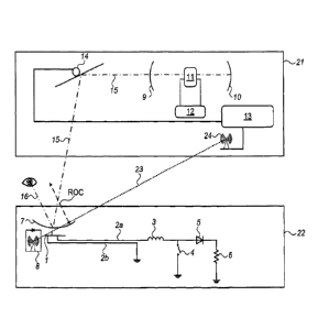
Reference is now made to Fig. 16, which is a schematic diagram showing a
detailed
description of the complete system. The system comprises transmitter 21 and
receiver 22.
In general, the transmitter and receiver will be located remotely from each
other, but are
shown in Fig. 16, for convenience, to be close to each other. Beam 15
transfers power from
transmitter 21 to receiver 22.
On the receiver 22, the front surface 7 reflects a small part of incident beam
15 as a
reflected beam 16, while either diffusing it or creating a virtual focal point
behind front
surface 7, or a real focal point at least lcm in front of surface 7. After
transmission through
the at least partially transparent surface 7, beam 15 impinges on the optical-
to-electrical
power converter 1.
The optical-to-electrical power converter 1 may be enclosed in a package that
may have a
front window, which may be surface 7 or a separate window. It may also be
coated to have
an external surface adapted to function as an interface with the air, or the
adhesive or the
glass surrounding it. In a typical configuration, the optical-to-electrical
power converter 1
could be a junction of semiconductor layers, which typically have conductors
deposited on
them. In many embodiments surface 7 would be coated on, or be the external
surface of
one of these semiconductor layers.
Signalling detector 8 indicates that beam 15 is impinging on photovoltaic cell
1 and
transmits that information to the controller 13, in this example system,
located in the
transmitter 21. The control signal is transmitted by a link 23 to a detector
24 on the
transmitter.
Electrical power converter 1, has a bandgap E8 and typically yields a voltage
between 0.35
and 1.1V, though the use of multi-junction photovoltaic cells may yield higher
voltages.
Power flows from the photovoltaic cell 1 through conductors 2a and 2b, which
have low
resistance, into inductor 3 which stores some of the energy flowing through it
in a
magnetic field.
Automatic switch 4, typically a MOSFET transistor connected to a control
circuit (not
shown in Fig. 16), switches between alternating states, allowing the current
to flow through
the inductor 3 to the ground for a first portion of the time, and for a second
portion of the
CA 02992681 2018-01-16
WO 2017/009854 PCT/1L2016/050776
31
time, allowing the inductor to emit its stored magnetic energy as a current at
a higher
voltage than that of the photovoltaic cell, through diode 5 and into load 6,
which can then
use the power.
Automatic switch 4 may be operating at a fixed frequency or at variable
frequency and/or
duty cycle and/or wave shape which may either be controlled from the
transmitter, or be
controlled from the client load, or be based on the current, voltage, or
temperature at the
load, or be based on the current, voltage or temperature at automatic switch
4, or be based
on the current, voltage or temperature emitted by the optical-to-electrical
power converter
1, or be based on some other indicator as to the state of the system.
The receiver may be connected to the load 6 directly, as shown in Fig. 16, or
the load 6 can
be external to the receiver, or it may even be a separate device such as a
cellphone or other
power consuming device, and it may be connected using a socket such as
USB/Micro
USB/Lightning/ USB type C.
In most cases there would also be an energy storage device, such as a
capacitor or a battery
connected in parallel to load 6, or load 6 may include an energy storage
device such as a
capacitor or a battery.
Transmitter 21 generates and directs beam 15 to the receiver 22. In a first
mode of
operation, transmitter 21 seeks the presence of receivers 22 either using a
scanning beam,
or by detecting the receiver using communication means, such as RF, Light, IR
light, UV
light, or sound, or by using a camera to detect a visual indicator of the
receivers, such as a
retro-reflector, or retro-reflective structure, bar-code, high contrast
pattern or other visual
indicator. When a coarse location is found, the beam 15, typically at low
power, scans the
approximate area around receiver 22. During such a scan, the beam 15 impinges
on
photovoltaic cell 1. When beam 15 impinges on photovoltaic cell 1, detector 8
detects it
and signals controller 13 accordingly.
Controller 13 responds to such a signal by either or both of instructing laser
driver 12 to
change the power P it inputs into gain medium 11 and or instructing mirror 14
to alter
either its scan speed or direction it directs the beam to or to hold its
position, changing the
scan step speed. When gain medium 11 receives a different power P from the
laser power
CA 02992681 2018-01-16
WO 2017/009854 32 PCT/1L2016/050776
supply 12, its small signal gain - the gain a single photon experiences when
it transverses
the gain medium, and no other photons traverse the gain medium at the same
time, -
changes. When a photon, directed in a direction between back mirror 10 and
output coupler
9 passes through gain medium 11, more photons are emitted in the same
direction ¨ that of
beam 15 - and generate optical resonance between back mirror 10 and output
coupler 9.
Output coupler 9 is a partially transmitting mirror, having reflectance R,
operating at least
on part of the spectrum between the first overtone of the C-H absorption at
6940 cm-1 and
the second overtone of the C-H absorption at 8130cm-1, and is typically a
multilayer
dielectric or semiconductor coating, in which alternating layers of different
refractive index
materials are deposited on a substrate, which is typically glass, plastic or
the surface of
gain medium 11. Alternatively Fresnel reflection can be used if the gain
medium is capable
of providing sufficient small signal gain or has a high enough refractive
index, or regular
metallic mirrors can be used. A Bragg reflector may also be used, should the
gain medium
be either a semiconductor or a fibre amplifier. Output coupler 9 may also be
composed of a
high reflectance mirror combined with a beam extractor, such as a semi-
transparent optical
component that transmits a part of the light and extracts another part of the
light from the
forward traveling wave inside the resonator, but typically also a third
portion extracted
from the backwards propagating wave inside the resonator.
Back reflector 10 should be a high reflectance mirror, although a small amount
of light
may back-leak from it and may be used for monitoring or other purposes,
working at least
on part of the spectrum between the first overtone of the C-H absorption at
6940 cm-1 and
the second overtone of the C-H absorption at 8130cm1. It may typically be
constructed of
alternating layers of different refractive index materials deposited on a
substrate, usually
glass, metal or plastic. Alternatively Fresnel reflection can be used if the
gain medium is
capable of providing sufficient small signal gain, or regular metallic mirrors
can be used. A
Bragg reflector may also be used should the gain medium be either a
semiconductor or a
fibre amplifier.
Gain medium 11 amplifies radiation between the first overtone of the C-H
absorption at
6940 cm-1 and the second overtone of the C-H absorption at 8130cm-1, although
not
necessarily over the whole of this spectral range. It is capable of delivering
small signal
gain larger than the loss caused by output coupler 9 when pumped with power P
by laser
CA 02992681 2018-01-16
WO 2017/009854 33 PCT/1L2016/050776
driver 12. Its area, field of view, and damage thresholds should be large
enough to
maintain a beam of at least 8kW/m2/Steradian/(1-R), where R is the reflectance
of output
coupler 9. It may be constructed of either a semiconductor material having a
bandgap
between 0.8-1.1eV or of a transparent host material doped with Nd ions, or of
another
structure capable of stimulated emission in that spectral range. Gain medium
11 is
positioned in the optical line of sight from the back reflector 10 to output
coupler 9, thus
allowing radiation reflected by the back reflector 10 to resonate between the
back reflector
and the output coupler 9 through gain medium 11.
For the exemplary implementation where the gain medium 11 is a semiconductor
having a
bandgap between 0.8-1.1eV, it should be preferably attached to a heat
extracting device,
and may be pumped either electrically or optically by laser driver 12.
In the exemplary implementation where the gain medium 11 is a transparent
host, such as
YAG, YV04, GGG, or glass or ceramics, doped with Nd ions, then gain medium 11
should
preferably also be in optical communication with a filter for extracting
radiation around
9400 cm-1 from that resonating between back mirror 10 and output coupler 9.
The beam steering apparatus 14 is shown controlled by controller 13. It can
deflect beam
into a plurality of directions. Its area should be large enough so that it
would contain
essentially most of beam 15 even when tilted to its maximal operational tilt
angle. Taking a
simplistic 2D example, if beam 15 were to be a collimated 5mm diameter (1/e2
diameter)
Gaussian beam, and the beam steering apparatus were to be a single round
gimballed
mirror centred on the beam centre, and if the maximal tilt required of the
mirror is 30
degrees, and assuming that beam steering apparatus 14 has no other apertures,
then if the
mirror has a 5mm diameter like that of the beam, it would have an
approximately 13% loss
at normal incidence to the beam, but approximately 60% loss at 60 degrees tilt
angle. This
would severely damage the system's performance. This power loss is illustrated
in the
graph of Fig. 17.
At the beginning of operation, controller 13 commands laser driver 12 and
mirror 14 to
perform a seek operation. This may be done by aiming beam 15, with the laser
driver 12
operating in a first state, towards the general directions where a receiver 22
is likely to be
found. For example, in the case of a transmitter mounted in a ceiling corner
of a room, the
CA 02992681 2018-01-16
WO 2017/009854 34 PCT/1L2016/050776
scan would be performed downwards and between the two adjacent walls of the
room.
Should beam 15 hit a receiver 22 containing an optical-to-electric power
converter 1, then
detector 8 would signal as such to controller 13. So long as no such signal is
received,
controller 13 commands beam steering 14 to continue directing beam 15 in other
directions, searching for a receiver. If such a signal is received from
detector 8, then
controller 13 may command beam steering 14 to stop or slow down its scan to
lock onto
the receiver, and to instruct laser driver 12 to increase its power emission.
Alternatively
controller 13 may note the position of receiver 22 and return to it at a later
stage.
When laser driver 12 increases its power emission, the small signal gain of
gain medium
11 increases, and as a result beam 15 carries more power and power
transmission begins.
Should detector 8 detect a power loss greater than a threshold, which may be
pre-
determined or dynamically set, and which is typically at a level representing
a significant
portion of the maximal permissible exposure level, and which is also typically
greater than
the system noise figure, these conditions implying either that beam 15 is no
longer aimed
correctly at the optical-to-electrical power converter 1, or that some object
has entered the
beam's path, or that a malfunction has happened, controller 13 should normally
command
laser driver 12 to change its state, by reducing power to maintain the
required safety level.
If another indication of safe operation is present, such as an indication from
the user as to
the safety of transmission, which may be indicated by a user interface or an
API, or an
indication of safe operation from a second safety system, the controller may
command the
laser to increase power to compensate for the power loss. The controller 13
may also
command the beam steering assembly 14 to perform a seeking operation again.
There may be two different stages in the seek operation. Firstly, a coarse
search can be
performed using a camera, which may search for visual patterns, for a retro
reflector, for
high contrast images, for a response signal from receivers or for other
indicators, or by
using the scanning feature of beam steering 14. A list of potential positions
where receivers
may be found can thus be generated. The second stage is a fine seek, in which
the beam
steering mirror 14 directs beam 15 in a smaller area until detector 8 signals
that beam 15 is
impinging on an optical-to-electrical power converter 1.
Reference is now made to Fig. 18, shows an example cooling system for the gain
medium
11 of the system of Fig. 16. Although the reflectors 9, 10 are shown as
separate optical
CA 02992681 2018-01-16
WO 2017/009854 35 PCT/1L2016/050776
elements, it is to be understood that one or both of them may be coated
directly on the gain
medium end faces for simplifying the system. Gain medium 11 converts the power
it
receives from the laser driver 12 into both heat and photons, and would
typically degrade
the system performance if the gain medium were to be heated above a certain
temperature.
For that reason, gain medium 11 is attached to heatsink 34 using a bonding
agent 33 which
is preferably a heat conducting solder having low thermal resistance. Bonding
agent 33
may also be a conductive adhesive. Bonding agent 33 may have a thermal
expansion
coefficient which is between that of gain medium 11 and heat sink 34. Heat
sink 34 may
typically be a low thermal resistance heatsink made out of metal, which may be
equipped
with fins for increasing its surface area or an external fluid pumping system
such as a fan
or a liquid pump 35.
It is appreciated by persons skilled in the art that the present invention is
not limited by
what has been particularly shown and described hereinabove. Rather the scope
of the
present invention includes both combinations and subcombinations of various
features
described hereinabove as well as variations and modifications thereto which
would occur
to a person of skill in the art upon reading the above description and which
are not in the
prior art.