Note: Descriptions are shown in the official language in which they were submitted.
CA 02993732 2018-01-25
=
1
METHOD FOR CONTROLLING AN ACTIVE PIXEL IMAGE SENSOR
TECHNICAL FIELD
The invention relates to electronic image sensors the operation of
which employs active pixels in MOS technology. More precisely, the invention
relates to a method for controlling the various transistors which make up the
active
pixel.
PRIOR ART
Active pixels most often comprise a photodiode that converts received
photons into electric charge, and a plurality of MOS transistors allowing the
read-
out of this charge and its conversion to electrical voltage to be controlled.
In a
matrix-array sensor, the rows of pixels are addressed individually and the
voltages
output by the pixels are applied to column conductors common to the pixels of
a
given column. Read-out circuits at the bottom of the column allow the voltages
present on the columns to be read out and converted to digital form. For
example,
for each addressed row of pixels, the voltages present on the columns are
sampled. The samples are stored in capacitors of the read-out circuit. The
samples are then converted into digital form by an analogue-to-digital
converter
(for example one converter for each column of pixels).
Active pixels using a photodiode generally comprise at least four
transistors: a transfer transistor serves to transfer the charge from the
photodiode
to what is called a read-out node, which is a capacitive charge-storage node;
a
read-out transistor, which is connected in a voltage follower configuration
and the
gate of which is connected to the read-out node in order to bring its source
to a
voltage representing the voltage of this node; a row-selection transistor
controlled
by a row conductor, for selecting an entire row of pixels and connecting the
output
of the follower transistor of each pixel to the column conductor corresponding
to
this pixel and, thereby, to the read-out circuit at the bottom of the column;
and a
reset transistor allowing the potential of the read-out node to be reset to a
reference value.
The amount of charge generated by the photodiode is measured by
calculating the difference between the potential level of the read-out node
obtained after the transfer, and the reference potential level obtained after
the
read-out node is reset.
CA 02993732 2018-01-25
2
Active-pixel structures may be controlled in various ways. In particular,
images may be captured using what is called the global shutter technique, in
which all the pixels integrate charge generated by light during an integration
period that is the same for all the pixels. Next, the pixels are read out row
by row.
In the technique called the rolling shutter technique, the integration period
is
shifted in time from one row of pixels to the next.
The global shutter technique especially makes it possible to avoid
distortion effects when images of moving objects are captured.
In an active-pixel structure comprising four or five transistors, the
sequence of the phase of integration common to all the pixels is the
following:
- for the time of an initialization control pulse, charge is forced out of all
the photodiodes. The end of this pulse sets the start of the integration
duration of
the photodiodes: they may once more accumulate the charge generated under
the effect of the light to which they are exposed. Charge may be removed by
simultaneously turning on, for the time of the initialization pulse, the
transfer
transistor and reset transistor of the read-out node. The charge is then
removed to
the drain of the reset transistor. However, it is generally preferred to use a
specific
fifth transistor, the source of which is connected to the photodiode of the
pixel, the
charge being removed to the drain of this transistor.
- all the transfer transistors are turned on simultaneously, for the time of
a control pulse applied to their gates: the charge generated and accumulated
by
each photodiode from the start of the current integration duration is
transferred to
the associated read-out node. It is the end of this transfer control pulse
that sets
the end of the integration duration for all the pixels.
After each integration duration, the read-out phase of the pixels may
start. The read-out is carried out sequentially, row by row. For each of the
pixels of
a row, the selection transistor of the pixel is turned on, for the time of a
selection
control pulse, and during this time:
- the signal level applied to the column conductor is sampled by the
read-out circuit located at the bottom of the column of the pixel; then
- the reset transistor of the read-out node is turned on, for the time of a
reset control pulse, and the reference level applied to the column conductor
is
sampled by the read-out circuit.
CA 02993732 2018-01-25
3
The read-out circuit may then deliver as output a measurement of the
difference between the signal level and the reference level. However, this
level is
not a precise measurement of the amount of charge generated in the photodiode
because the random noise called kTC noise is not removed. Indeed, this noise
is
generated by the reset of the read-out node by the reset transistor, and means
that the potential applied to the read-out node is not absolutely certain.
If this uncertainty is to be removable, with the aim of increasing the
dynamic range of the sensors to encompass low light levels, it is necessary
for the
signal level to be applied to the read-out node after it has been reset, so
that this
signal level takes into account this uncertainty. In other words, it is
necessary to
initialize the read-out node first, sample the corresponding reference
potential
level, then apply the signal level (transfer) and next sample the signal
level. A
correlated double sampling (CDS) read-out is spoken of. With a four- or five-
transistor structure such as described, a CDS read-out is only possible in a
rolling-
shutter integration mode. A CDS read-out is not possible in global-shutter
integration mode.
Thus, in the prior art, structures including a memory node between the
photodiode and the read-out node have been proposed. The memory node makes
it possible to store the charge generated by the photodiode after each of the
durations of integration common to all the pixels, for the time it takes, in
each row
of pixels, to initialize the read-out node of each of the pixels, and to
sample the
corresponding reference level with the read-out circuit of each of the pixels
of the
row, then to transfer the charge from the memory node to the read-out node and
to sample the signal level with the read-out circuit. These structures
comprising an
intermediate memory stage thus make it possible to employ both the global-
shutter capture technique and correlated double sampling, allowing the amount
of
charge generated in the photodiode of each of the pixels, during the
integration
duration in question, to be precisely measured. In practice, provision is then
made
for two transfer transistors (or gates), a first between the photodiode and
the
memory node and a second between the memory node and the read-out node.
The first transfer transistor between the photodiode and the memory node is
then
the transistor that controls the end of each integration duration for all the
pixels at
the same time, this end coinciding with the end of the transfer control pulse
in the
memory node. The second transfer transistor is employed in the pixel-row read-
out phase.
CA 02993732 2018-01-25
4
Publication US 2014/0247378 proposes another use of the memory-
node pixel structure, to adjust the exposure duration of the photodiodes, for
example depending on the colour of the pixels and on the intensity of the
light. It is
a question of controlling one or more sub-periods of exposure of the
photodiodes
during the duration of each acquisition cycle. The duration of each sub-period
is a
fraction of the duration of the cycle, and the actual exposure duration,
during
which the pixel accumulates charge, is equal to the sum of the durations of
the
sub-periods of the pixel and shorter than the duration of the cycle.
In the present invention, it is these active-pixel structures including a
memory node between the photodiode and the read-out node, which structures
are suitable for providing a correlated double sampling read-out function,
that are
addressed. These structures, examples of which may be found in publications
FR2961631 and JP20063115150, allow both an image to be captured by all the
pixels simultaneously in the same integration duration (global shutter
function) and
a CDS read-out of the pixels, row by row.
These structures have a dynamic range that is optimized at the low
end, since they are low read-out noise structures (CDS read-out).
In the presence of bright light there is however a risk of saturation of
the photodiode, this limiting dynamic range at the high end. Now, the maximum
storage capacity of photodiodes depends on the area occupied by the
photodiode,
which for its part determines the size of the pixel. It is certainly not
desired to
increase this size; the tendency is even rather to decrease it, and to
compensate
for the loss of aperture by using microlenses to concentrate the light on the
photodiodes of the pixels.
SUMMARY OF THE INVENTION
According to the invention, to improve the high-end dynamic range of
these sensors, it is proposed to adopt the two following measures:
- on the one hand, provision is made for the charge-storage capacity of
the memory node to be at least N times higher than the charge-storage capacity
of the photodiode (N being an integer higher than or equal to 2); and
- on the other hand, provision is made to perform N transfers of charge
from the photodiode to the memory node, said transfers being regularly spaced
over the integration duration.
CA 02993732 2018-01-25
It is in general easy to provide a memory node having a storage
capacity a plurality of times higher than the storage capacity of the
photodiode
without this leading to too great a reduction in the optical aperture of the
pixel.
Specifically, the memory node may be formed by an insulated gate, the
5 capacitance per unit area of which is very much higher than the capacitance
per
unit area of the photodiode.
Thus, the invention relates to a method for taking images with an
active-pixel sensor comprising at least one row of active pixels in which
sensor the
active pixels each comprise a photosensitive element, a read-out node and a
memory node between the photosensitive element and the read-out node, and at
least one first charge-transfer transistor between the photosensitive element
and
the memory node, one second charge-transfer transistor between the memory
node and the read-out node, one transistor for resetting the read-out node,
one
follower transistor having its gate connected to the read-out node and one
pixel-
selection transistor that is connected between the source of the follower
transistor
and a column conductor, the displaying method being such that each integration
and read-out cycle comprises an integration duration common to all the pixels
allowing, in each pixel, the accumulation of photogenerated charge by the
photosensitive element of the pixel throughout the integration duration, then
a
correlated double sampling read-out phase in which the pixels of each row are
successively read out. For each integration and read-out cycle, the image-
taking
method commands a reset of all the photosensitive elements simultaneously by
applying an initialization control pulse, and the end of said pulse sets the
start of
the integration duration common to all the pixels, allowing, in each pixel,
the
accumulation of photogenerated charge by the photosensitive element of the
pixel
throughout said integration duration, and, during the common integration
duration,
the image-taking method commands, simultaneously in all the pixels, N
regularly
spaced transfers of charge from the photosensitive element to the memory node,
N being an integer higher than or equal to 2, the memory node being configured
to have a charge-storage capacity that is at least N times that of the
photosensitive element, the N transfers being obtained by applying, at regular
intervals during said common integration duration, N control pulses to the
gate of
the first transfer transistor, and the end of the Nth transfer setting the end
of the
common integration duration.
CA 02993732 2018-01-25
6
Preferably, the read-out node has at least N times the charge-storage
capacity of the photosensitive element
Preferably, N is chosen equal to 2 or 3.
Other features and advantages of the invention are presented in the
following description, with reference to the appended drawings, in which:
- Figure 1 illustrates a general active-pixel structure to which the
invention may be applied;
- Figure 2 is a timing diagram of the control signals of an active pixel
implementing an image-taking method according to the invention;
- Figures 3a to 3d show diagrams of the potentials in the structure of
the pixel corresponding to various steps a) to d) of the integration duration;
and
- Figures 4a to 4c show diagrams of the potentials in the structure of
the pixel corresponding to various steps a') to c') of the read-out phase.
DETAILED DESCRIPTION
Active pixels are produced in CMOS technology in a doped (for
example p-doped) active semiconductor layer and in addition comprise
photodiodes, which are in principle what are called pinned photodiodes,
capacitive
storage nodes and transistors. Embodiments thereof employ various CMOS
technologies well known to those skilled in the art.
In this description, a substrate with a p-doped active semiconductor
layer, which substrate is biased to a zero reference potential and the
circuits of
which are supplied with a positive supply voltage denoted Vdd, is described.
Those skilled in the art will know that it is necessary to invert the biases
if a
substrate with an n-doped active semiconductor layer is used.
Figure 1 is an equivalent circuit of a general structure of an active pixel
comprising a photosensitive element, memory node and read-out node, to which
structure the invention may be applied. In this example, the pixel PIX
comprises a
photodiode PHD, a first capacitive storage node called the memory node and
referenced MN, a second capacitive storage node called the read-out node and
referenced SN and at least 5 transistors that are:
- a first transfer transistor TRAi (in practice a simple transistor gate),
allowing charge to be transferred from the photodiode PHD to the memory node
MN.
CA 02993732 2018-01-25
7
- a second transfer transistor TRA2 (in practice a simple transistor
gate), allowing the memory node MN to be emptied into the read-out node.
- a transistor RST for resetting the read-out node SN, the source of
which is electrically connected to the read-out node and the drain of which is
connected to the positive supply voltage Vdd.
- a follower transistor SF, the gate of which is electrically connected to
the read-out node SF, and the drain of which is biased to the supply voltage
Vdd.
- a selection transistor SEL the gate of which receives a pixel-row
selection command, the drain of which is electrically connected to the source
of
the follower transistor and the source of which is connected to a column
conductor
(Col) of the matrix array (the pixels being arrayed in a matrix of rows of
pixels and
columns of pixels), each column conductor being connected, at the bottom of
the
column, to a read-out circuit CL common to all the pixels of the column.
It may comprise a sixth transistor AB, which allows the photodiode to
be initialized, by allowing charge to be removed via its drain. One advantage
of
this sixth transistor is that it enables what is called an anti-blooming
function, i.e.
by biasing its gate to a set voltage under the threshold voltage of the
transistor, it
is possible to adjust the potential of the barrier of the semiconductor region
under
the gate to a level that allows excess charge to be removed from the
photodiode
via the drain of the transistor. When it is not provided, the photodiodes are
initialized by activating, together in each pixel, the transistors TRAi, TRA2
and
RST.
It will be noted that certain transistors of the pixel may in practice be
shared between at least two pixels, this possibly being advantageous when it
is
sought to produce small pixels with a high fill factor. For example, the
follower
transistor and the row-selection transistor are shared between two or four
pixels of
a given column. The photodiode-initialization transistor may also be shared
between at least two pixels. The area of active layer required to control the
pixels
is thus decreased. The invention also applies to these shared-transistor pixel
structures.
The photodiode PHD is usually a pinned photodiode pinned to a
voltage denoted Vpin and defined by the technology, i.e. it includes, in the n-
type
diffusion region, a superficial p-type diffusion region and the superficial
region is
brought to the (zero) reference potential of the substrate.
CA 02993732 2018-01-25
8
The read-out node SN, which is the equivalent of a capacitor, in
practice consists of a floating n-doped semiconductor region. The charge-
storage
capacity of the read-out node at least corresponds to that of the photodiode.
This
capacity especially depends on the dopant concentration and the geometry of
the
memory node.
The memory node MN is the equivalent of a capacitor for storing the
charge generated and accumulated by the photodiode at the end of an
integration
period. In practice, this memory node is not a floating diffusion like the
read-out
node. Specifically, it must be possible to set its potential to a given level
that must
be higher than the photodiode voltage Vpin, at least in the phase of transfer
of
charge from the photodiode to the memory node; and which must be lower than
the supply voltage Vdd, at least in the phase of transfer of charge from the
memory node to the read-out node. Its potential may therefore change,
depending
on the phase in question, i.e. depending on whether the memory node is the
source or the destination of the transferred charge. But it may also be set.
In the
rest of the description, and in the drawings, it is this option (set
potential) that is
shown, for the sake of greater simplicity.
For example, the memory node is a semiconductor region surmounted
by a gate, and this gate is biased to a potential that allows a given
potential level
between the level Von of the photodiode and Vdd to be applied to the memory-
node semiconductor region under the gate. The charge-storage capacity under
this gate then depends on the gate capacitance (and therefore its geometry),
on
the dopant concentration, etc. Other exemplary embodiments of memory nodes
may be found in the prior art of what are called (at least) six-transistor
pixels ; for
example, patent publications W02006130443, U8598629 and FR2961631.
In an example in which the substrate is p-type, these various transistors
will be nMOS transistors, i.e. they will have source and drain regions that
are n-
type diffusions on either side of a p-type channel under the gate.
The term "transistor" is used to facilitate comprehension in terms of an
equivalent circuit diagram such as the diagram in Figure 1. However, in the
physical make-up of the pixel, these transistors are not necessarily all
formed in
the conventional way, independently of the other elements of the pixel, with a
source region, a drain region, a channel region separating the source from the
drain and an insulated gate on top of the channel. In the actual physical make-
up
CA 02993732 2018-01-25
9
of the pixel, certain transistors in fact essentially consist of an insulated
gate to
which a control potential may be applied. Thus, for example, the first
transfer
transistor TRA1 will consist of a simple transfer gate TRA1-g insulated from
the
substrate, surmounting a p-type channel region that is located between the n-
type
photodiode PHD region (source of TRA1) and the n-type region of the memory
node NM (drain of TRA1). Likewise: the source of the second transfer
transistor
TRA2 may be the n-type region of the memory node NM, and the drain of this
transistor TRA2 may be the n-type region of the read-out node SN. Furthermore,
the source of the initialization transistor AB may be the n-type region of the
photodiode that accumulates the charge generated by the light; and the source
of
the transistor RST may be the n-type region of the read-out node.
The invention does not relate to a particular active-pixel technology, but
indeed to the use of an active-pixel structure comprising a photodiode, a read-
out
node and a memory node between the photodiode and read-out node and, for
example, to a structure such as described above, with or without an anti-
blooming
transistor AB. Furthermore, the active-pixel structure may comprise one or
more
transistors shared with at least one other pixel.
In the invention, provision is made, as regards control of the active
pixel, for the following two measures:
- the charge-storage capacity of the memory node is at least N times
higher than the charge-storage capacity of the photodiode (N being an integer
higher than or equal to 2); and
- charge is transferred N times from the photodiode to the memory
node, these transfers being regularly spaced, during each integration duration
of a
periodic charge integration and read-out cycle.
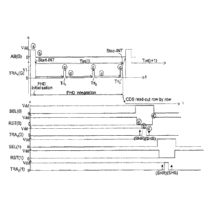
Thus, as illustrated by the timing diagram in Figure 2 for an example in
which N is equal to 3, after the start of the integration duration Tint(i) of
an ith
integration and read-out cycle, which start is set by the falling edge of the
gate
control pulse AB-g of the photodiode-initialization transistor AB, N=3 control
pulses
Trii, Tri2 and Tri3 are applied in succession, at regular intervals, to the
gate TRAi-
g of the first transfer transistor TRA1. The falling edge of the last (Nth)
pulse Tri3
marks the end of the current integration duration Tint(i).
In this way, in case of high light levels, as charge is transferred a
plurality of times during the integration period, the photodiode will be able
to
continue to accumulate charge throughout the integration duration; the charge
is
CA 02993732 2018-01-25
added in the memory node on each transfer. The transfers are carried out at
regular intervals that are equally distributed over the integration duration
Tint. In
other words, in this example in which N=3, the time interval between the start
of
integration and the 1st transfer, between the 1st and 2nd transfers, and
between
5 the 2nd and 3rd transfers, is substantially the same.
The two measures of the invention allow a method for controlling pixels
to be implemented that has the technical effect of multiplying by N the charge
accumulation capacity in each pixel over the duration of the integration
period for
a given photodiode capacity. However, this accumulation does not occur in the
10 photodiode. In the invention, this accumulation occurs in the memory node,
because charge is transferred at regular intervals from the photodiode to the
memory node throughout the integration duration. As indicated above, the
memory node is not subject to the same technological limitations as the
photodiode: therefore it is possible to produce a memory node with the desired
storage capacity, at least equal to N times the capacity of the photodiode,
without
adversely affecting the size of the pixel.
The read-out node also preferably has, for its part, a capacity at least
equal to N times that of the photodiode.
Preferably, N is equal to 2 or 3.
An active-pixel sensor having the general (electrical) structure in Figure
1 is especially suitable for an image-taking method employing an integration
duration that is common to all the pixels (global shutter) and a row-by-row
correlated double sampling (CDS) read-out of the pixels by the read-out
circuit at
the bottom of each column.
The control method according to the invention, which uses a memory
node the capacity of which is at least N times that of the photodiode, is
particularly
suitable and advantageous for such an image-taking method.
Such an image-taking method is now described with reference to the
timing diagram of the control signals of the transistors, which diagram is
shown in
Figure 2, and the diagrams of potentials in Figures 3 and 4. In Figures 3 and
4,
the value of the potential of the various gates, which are represented by
rectangles, is indicated by the fill colour of each rectangle: white=zero;
black=Vdd;
grey=intermediate potential. Furthermore, to facilitate comprehension, the
steps
and the Figures 3 or 4 that correspond to these steps are referenced by one
and
CA 02993732 2018-01-25
11
the same letter. Lastly, it will be noted that the timing diagrams and
potential-
barrier representation in Figures 2 to 4 correspond to a context in which the
sensor is produced in a p-type active layer. Those skilled in the art will be
able
make the conversion to a context in which the active layer is n-type.
An initial state (not shown in Figures 3 and 4) is started from, in which
state the transistors are all in the off state.
Each periodic integration and read-out cycle comprises an integration
duration Tint common to all the pixels, then a CDS read-out of the pixels, row
by
row.
As illustrated in Figure 2, each integration and read-out cycle starts with
a step a) of initializing all the photodiodes simultaneously. A corresponding
diagram of the potentials in the structure is illustrated in Figure 3a.
In this step, an initialization control pulse AB(G) is applied
simultaneously to the gates AB-g of all the initialization transistors AB:
these are
then fully turned on and empty the associated photodiode of all charge, via
the
drain DAB of the associated transistor. In a structure without an anti-
blooming
transistor AB, the photodiodes would be initialized by simultaneously turning
on,
for the time of the initialization pulse, the first and second transfer
transistors and
the reset transistor of the read-out node. The charge would then be evacuated
to
the drain of the reset transistor.
The end of the common initialization pulse AB(G) causes the
transistors AB to return to the off state and sets the start Start-INT of the
integration duration Tint(i) for all the photodiodes PHD simultaneously: the
photodiodes may, from this moment in time, once again accumulate the charge
generated under the effect of the light to which they are exposed. This is
step b)
illustrated in Figures 2 and 3b.
The following step c) (Figures 2 and 3c) consists in applying via the
control signal TRA1(G) applied to all the gates TRAi-g of the pixels, a first
control
pulse Trii: the first transfer transistors TRAi are at this moment fully
turned on,
and the charge generated and accumulated by each photodiode from the start
Start-INT of the current integration duration is transferred to the associated
memory node. In the example, the voltage level corresponding to the active
state
of the control pulse Trii is a level V1 intermediate between 0 and Vdd, in
order to
lower the potential barrier of the semiconductor region under the gate TRAi-g
to a
level that allows the charge to transfer from the photodiode to the memory
node.
CA 02993732 2018-01-25
12
At the end of the control pulse Trii, the photodiode again begins to
accumulate charge: this is step d) (Figures 2 and 3d), until the next control
pulse
Tri2.
Thus, steps c) and d) are applied to all the pixels simultaneously and
are repeated in succession until the Nth transfer pulse, which is the 3rd
pulse Tri3
in the example illustrated in Figure 2: the end of this Nth pulse marks the
end
Stop-INT of the current integration duration Tint(i).
A new integration duration Tint(i+1) of a new periodic cycle (of
integration then read-out) may then start, repeating the steps a, b, c and d
described above.
With the end Stop-INT of the current integration duration Tint(i), the
following phase of read-out of the pixels may start. It is a sequential row-by-
row
read-out. The pixels of a row are selected by applying a selection control
pulse to
the gate SEL-g of the selection transistor SEL of each pixel (Figure 2: signal
SEL(0) for the first row of rank 0), this causing, for each pixel of the
selected row,
the source of the follower transistor SF of the pixel to be electrically
connected to
the corresponding column conductor and therefore to the corresponding read-out
circuit CL, for the time of this selection pulse. The CDS read-out of the
pixels of
the selected row is carried out during this selection time, and comprises the
series
of following steps a') to d'):
- a') the gate RST-g of the reset transistor of the read-out node of each
of the pixels of the selected row is drawn to the zero potential (Figure 2:
control
signal RST(0) at zero for the row of rank 0), this gate being maintained at
Vdd
otherwise. The potential on the column conductor then reaches a reference
level
that is sampled by the read-out circuit at the bottom of the column. This
sampling
is represented in Figures 2 and 4a by the signal SHR.
- b') the second transfer transistor TRA2 of each pixel of the selected
row is turned on, for the time of a control pulse of level Vdd, which is
applied to
their gate TRA2-g (signal TRA2(0) for the selected row of rank 0 - Figure 2),
allowing charge to be transferred from the memory node to the read-out node
(Figures 2 and 4b).
- c') at the end of this transfer pulse, the potential of the column
conductor reaches a signal level representative of the amount of charge on the
read-out node, and this signal level is sampled by the read-out circuit at the
bottom of the column (SHS, Figures 2 and 4c).
CA 02993732 2018-01-25
13
- d') the gate RST-g of the transistor is returned to the potential Vdd
(RST(0)=Vdd) then the row is deselected (end of the selection pulse SEL(0) -
Figure 2).
Steps a' to d' are applied simultaneously to all the pixels of the selected
row.
The sequence of read-out steps a') to d') is repeated for each of the
rows of pixels in succession, as illustrated in Figure 2, for the following
row of rank
1, with the corresponding control signals SEL(1), RST(1) and TRA2(1).
At the same time as the following read-out phase, an integration
duration Tint(i) is ongoing, or after this read-out phase, a new integration
duration
(Tint(i+1)) of a following integration and read-out cycle may start.
However, the read-out of all the rows must be terminated before the
first transfer pulse Tri1 produced after a duration Tint(i+1)/N following the
start of
the following integration duration Tint(i+1).
The invention just described allows the dynamic range of an active
pixel comprising an intermediate memory node between the photosensitive
element and the read-out node to be improved by obviating technological
constraints without increasing the area of the photosensitive element. It may
even
be envisaged to decrease this photosensitive-element area while compensating
for the loss of fill factor by using a microlens on each pixel to concentrate
the light
toward the photosensitive area of the pixel.
The invention is particularly advantageous for miniaturized sensors if it
is furthermore envisaged to implement it with memory-node technologies that
provide a capacitance per unit area that is intrinsically higher than that
achieved
with the technologies of pinned photodiodes.