Note: Descriptions are shown in the official language in which they were submitted.
CA 02993873 2018-01-26
P1149-1CA
1
Method and Apparatus for Collecting Signals, and Method and Apparatus for
Tracking
Cells by Using Light Sensitive Chip
Technical Field
[0001] The invention relates to the technical field of information
acquisition, in particular to a
method and apparatus for collecting signals, and method and apparatus for
tracking cells by
using light sensitive chip.
Background
[0002] Western blotting is a hybrid technique that combines high-resolution
gel
electrophoresis with immunochemical analysis technique. With advantages of
high analysis
capacity, high sensitivity and strong specificity, the western blotting is a
most common
method for detecting the characteristics, expression and distribution of
protein, such as
qualitative and quantitative detection of tissue antigen, mass measurement of
peptides and
antibody or antigen detection of virus.
[0003] The existing apparatus and method for collecting signals by the western
blotting are as
follows:
[0004] Method 1: tightly attaching a light sensitive film to an NC membrane,
developing and
marking them after exposing for a certain period, and displaying the image on
the film. The
advantages are high sensitivity and high resolution. The disadvantages are as
follows:
CA 02993873 2018-01-26
P1149-1CA
2
[0005] 1. Large occupied space: specialized dark room (room), sink and
sewer line are
required.
[0006] 2. High cost: processing machine, cassette and consumables such as
lots of light
sensitive films, developing solution and fixative solution should be
purchased. Washing of
films may waste water.
[0007] 3. Pollution of environment: much developing solution and fixative
solution are
required for developing films, and films discarded due to substandard quality
are produced at
the same time, causing heavy metal pollution and aromatic compound pollution.
[0008] 4. Unstable image quality: researcher cannot monitor exposure extent
in real time
in the dark room, but can get better images only after a few attempts. Mostly,
the
disadvantages are either underexposure or overexposure, and waste of time and
energy.
[0009] 5. Waste of time: since the current data are stored, transmitted and
published in
digital manner, the film images will be converted into digital images by
scanning.
[0010] 6. Quantitative inaccuracy: mostly, the images which are determined
as good by
researchers through visual inspection have been supersaturated in gray scale
in fact. So the
subsequent gray scale scanning is hard to quantify accurately.
[0011] Method 2: directly photographing samples by use of light sensitive
devices such as
CCD. The advantage is that all disadvantages in Method 1 are overcome. The
disadvantage is
the loss of the advantages of film collection, that is, the sensitivity is
severely reduced. The
reason is as follows: for all such devices on current market, a CCD digital
camera is mounted
CA 02993873 2018-01-26
P1149-1CA
3
above the NC film at a certain distance for shooting images. For light energy
radiated by a
light source, only the ray of light within a small angle can be collected by a
camera. But more
than 90% energy is lost. Therefore, such devices are often photographed under
strong light.
Only individual brands claim that they can be used for photographing WB under
low light.
Compared with the film, the exposure time is greatly extended. Some brands
reduce
resolution by pixel binning to improve sensitivity so as to reach the
sensitivity matching the
film. However, mosaics appear when the image is slightly magnified, and it is
hard to meet
various needs.
[0012] Method 3: scanning and collecting low light signals by CCD light
sensitive units
which are linearly aligned. The advantage is that the collection rate of
optical signals is
increased to improve the sensitivity. The disadvantages are as follows: since
the optical signal
is collected by linear scanning and the whole image cannot be collected at the
same time,
time difference appears during scanning of different regions. The intensities
of signals
collected on different time points are not comparable because the light source
is constantly
attenuated over time. Many control tests are not comparable.
[0013] Therefore, the technical problem to be urgently solved by those skilled
in the art at
present is how to innovatively provide an effective measure to solve the
existing problem and
meet more demands in actual applications.
Summary of the Invention
[0014] The technical problem to be solved in the embodiments of the invention
is to provide
a method and apparatus for collecting signals, and method and apparatus for
tracking cells by
using light sensitive chip to convert the signals to be detected from optical
signals into digital
signals and rapidly perform quantitative analysis.
CA 02993873 2018-01-26
P1149-1CA
4
[0015] Correspondingly, the embodiments of the invention also provide a
apparatus for
collecting signals by using light sensitive chip and an apparatus for tracking
cells to ensure
implementation and application of above method.
[0016] In order to solve the problems above, the invention discloses a method
for collecting
signals by using light sensitive chip, comprising the following steps:
[0017] closely fitting a luminous surface of a membrane carrying optical
signals to be
collected on a light sensitive chip;
[0018] placing the light sensitive chip fitted with the membrane carrying
optical signals to be
collected in a dark room which is not affected by external light;
[0019] collecting optical signals by the light sensitive chip in the dark
room;
[0020] processing and outputting the collected optical signals.
[0021] Preferably, the method for collecting optical signals by the light
sensitive chip in the
dark room comprises the following steps:
[0022] collecting optical signals;
[0023] observing exposure extent by a computer screen in real time;
[0024] stopping exposure when signals are accumulated to a predetermined
intensity;
CA 02993873 2018-01-26
P1149-1CA
[0025] obtaining and saving the image produced by exposure.
[0026] Preferably, when the signal collected by the light sensitive chip is a
western blotting
signal, the membrane carrying optical signals to be collected is obtained by
the following
steps:
[0027] conducting electrophoresis for the protein to be tested;
[0028] transferring the protein from a gel after completion of
electrophoresis;
[0029] transferring the protein to be tested from the gel to a polyvinylidene
fluoride
membrane or a nitrocellulose membrane;
[0030] sealing the POLYVINYLIDENE FLUORIDE membrane or the nitrocellulose
membrane after transfer, adding primary antibody reaction resisting the
protein to be tested,
and adding secondary antibody HRP reaction;
[0031] treating the reacted polyvinylidene fluoride membrane or nitrocellulose
membrane
with chemiluminescent liquid.
[0032] Preferably, the membrane comprises nitrocellulose membrane and\or
polyvinylidene
fluoride membrane.
[0033] Preferably, the light sensitive chip comprises CMOS light sensitive
chip and CCD
light sensitive chip.
CA 02993873 2018-01-26
P1149-1CA
6
[0034] The invention also discloses an apparatus for collecting signals by
using light
sensitive chip, comprising:
[0035] a fitting module for closely fitting a luminous surface of a membrane
carrying optical
signals to be collected on a light sensitive chip;
[0036] a laying module for placing the light sensitive chip fitted with the
membrane carrying
optical signals to be collected in a dark room which is not affected by
external light;
[0037] a signal collecting module for collecting optical signals by the light
sensitive chip in
the dark room;
[0038] a signal processing module for processing and outputting the collected
optical signals.
[0039] The invention also discloses a method for tracking cells by using light
sensitive chip,
comprising the following steps:
[0040] implanting cells or animals carrying luciferase on the light sensitive
chip;
[0041] placing the light sensitive chip implanted with cells or animals
carrying luciferase in a
dark room which is not affected by external light;
[0042] collecting optical signals by the light sensitive chip in the dark
room;
[0043] processing and outputting the collected optical signals.
CA 02993873 2018-01-26
P1149-1CA
7
[0044] Preferably, the method further comprises the following steps before
implanting cells
or animals carrying luciferase on the light sensitive chip: adding a glass
layer on the light
sensitive chip; and implanting the cells or animals carrying luciferase on the
glass layer of the
light sensitive chip.
[0044] Preferably, the method for obtaining the cells and animals carrying
luciferase
comprises the following steps:
[0045] constructing a reporter gene plasmid for inserting a specific fragment
of target
promoter into the front part of the luciferase expression sequence;
[0046] co-transfecting regulatory sequence and luciferase gene plasmid into
cells or the
fertilized eggs of animals;
[0047] adding luciferin to the cell culture medium.
[0048] The invention also discloses an apparatus for tracking cells by using
light sensitive
chip, comprising:
[0049] an implanting module for implanting cells or animals carrying
luciferase on the light
sensitive chip;
[0050] a laying module for placing the light sensitive chip implanted with
cells or animals
carrying luciferase in a dark room which is not affected by external light;
CA 02993873 2018-01-26
P1149-1CA
8
[0051] a signal collecting module for collecting optical signals by the light
sensitive chip in
the dark room;
[0052] a signal processing module for processing and outputting the collected
optical signals.
[0053] Compared with the prior art, the embodiments of the invention comprise
the following
advantages:
[0054] The scheme of the invention is to closely fit the luminous surface of
the membrane
carrying optical signals to be collected on the light sensitive chip, place
the light sensitive
chip fitted with the membrane carrying optical signals to be collected in the
dark room,
collect optical signals by the light sensitive chip in the dark room, and
process and output the
collected optical signals. Collection of signals by directly contacting the
light sensitive chip
can collect the whole image at the same time and greatly avoid the loss of
optical signals, so
as to improve the sensitivity without reducing the resolution.
[0055] It keeps all advantages of three methods in the background and avoids
respective
disadvantages.
Brief Description of the Drawings
[0056] In order to clearly describe the embodiments of the invention or the
technical scheme
in the prior art, the embodiments or drawings used in technical description
will be simply
introduced as follows. Apparently, the drawings described below are some
embodiments of
the invention. Those skilled in the art can obtain other drawings based on
these drawings
without creative work.
CA 02993873 2018-01-26
P1149-1CA
9
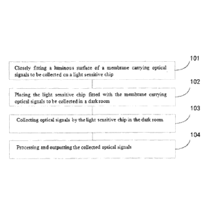
[0057] Fig. 1 is a process diagram of a method for collecting signals by using
light sensitive
chip;
[0058] Fig. 2 is a structural diagram of an apparatus for collecting signals
by using light
sensitive chip;
[0059] Fig. 3 is a process diagram of a method for tracking cells by using
light sensitive chip;
[0060] Fig. 4 is a structural diagram of an apparatus for tracking cells by
using light sensitive
chip;
Detailed Description of the Preferred Embodiments
[0061] In order to make objectives, technical scheme and advantages of the
embodiments of
the invention clearer, the technical scheme in the embodiments of the
invention will be
described clearly and completely in combination with the figures of the
embodiments as
follows. Apparently, the embodiments described are some but not all
embodiments of the
invention. Based on the embodiments of the invention, all other embodiments
obtained
without creative work by those skilled in the art shall fall within the
protection scope of the
invention.
[0062] Example 1
[0063] A method for collecting signals by using light sensitive chip of the
embodiments of
the invention is described in detail.
CA 02993873 2018-01-26
P1149-1CA
[0064] Referring to Fig. 1, a process diagram of the embodiments of a method
for collecting
signals by using light sensitive chip in the invention is shown, specifically
comprising
following steps:
[0065] Step 101, closely fitting a luminous surface of a membrane carrying
optical signals to
be collected on a light sensitive chip;
[0066] In actual application, when a western blotting signal is collected by
the light sensitive
chip, the membrane carrying optical signals to be collected is obtained by the
following steps:
[0067] conducting electrophoresis for the protein to be tested;
[0068] transferring the protein from a gel after completion of
electrophoresis;
[0069] transferring the protein to be tested from the gel to a polyvinylidene
fluoride
membrane or a nitrocellulose membrane;
[0070] sealing the polyvinylidene fluoride membrane or the nitrocellulose
membrane after
transfer, adding primary antibody reaction resisting the protein to be tested,
and adding
secondary antibody IIRP reaction;
[0071] treating the reacted polyvinylidene fluoride membrane or nitrocellulose
membrane
with chemiluminescent liquid.
[0072] In the application, the used membrane mainly comprises nitrocellulose
membrane
(NC membrane) and\or polyvinylidene fluoride membrane (PVDF membrane). The
used
CA 02993873 2018-01-26
P1149-1CA
11
light sensitive chip comprises CMOS light sensitive chip and CCD light
sensitive chip.
Considering that the light sensitive chip with large size has high
manufacturing cost, the array
of CMOS light sensitive chip and CCD light sensitive chip may be adopted to
greatly reduce
the cost if the chip splicing technique can achieve better effect in practice.
[0073] Step 102, placing the light sensitive chip fitted with the membrane
carrying optical
signals to be collected in a dark room which is not affected by external
light;
[0074] In order to avoid the influence of external light, the light sensitive
chip fitted with the
membrane carrying optical signals to be collected is placed in the dark room.
The
implementation method can be easily selected based on specific environment.
The chip can
be covered by a light blocking lid.
[0075] Step 103, collecting optical signals by the light sensitive chip in the
dark room;
[0076] In actual application, the method for collecting optical signals by the
light sensitive
chip in the dark room comprises the following steps:
[0077] collecting optical signals;
[0078] observing exposure extent by a computer screen in real time;
[0079] stopping exposure when signals are accumulated to a predetermined
intensity;
[0080] obtaining and saving the image produced by exposure.
CA 02993873 2018-01-26
P1149-1CA
12
[0081] Step 104, processing and outputting the collected optical signals.
[0082] Processors such as single chip, FPGA and CPU can be used for processing
and
outputting the collected optical signals. Due to the mature signal processing
method, the
signal processing in the scheme can be easily completed, which will not be
repeated herein.
[0083] =The western blotting signal (WB signal) collected by the light
sensitive chip is
described in detail in combination with actual application as follows:
[0084] Operating principles of the western blotting:
[0085] 1. Vertically separating cells or tissue extracts from the
polypropylene gel
using electric field;
[0086] 2. Horizontally transferring the protein band to the NC membrane
using
electric field, this band is called Blot if its relative position does not
change;
[0087] 3. Sealing. Soaking the blotted membrane in BSA solution. Filling
BSA
solution in the areas not occupied by the protein band. Avoiding the
subsequent antibodies
being adsorbed in these areas, and combining the antibody with its antigen
only.
[0088] 4. Incubation of antibody. Hinging the antibody with HRP in advance.
Soaking
the antibody with the NC membrane for incubation. Specifically combining the
antibody and
its antigen.
CA 02993873 2018-01-26
P1149-1CA
13
[0089] 5. Collection
of signals. Soaking the NC membrane in the solution containing
HRP substrate. Releasing fluoresce when its substrate is catalyzed with HRP.
Collecting
fluorescence signals by use of light sensitive film or electro-photographic
system.
[0090] Steps before collection of WB optical signals are as follows:
[0091] (1) Obtaining protein sample: after bacterial-induced expression,
directly splitting
cells by loading buffer via electrophoresis, adding homogenized buffer to
eukaryocyte, and
homogenizing them for 0.5-1min by machine or in ultrasonic room. Then
centrifuging
13,000g mixture for 15min at 4 C. Taking supernatant as a sample.
[0092] (2) Electrophoresis: preparing electrophoresis gel for SDS-PAGE.
[0093] (3) Transferring: 0 After electrophoresis, cutting the adhesive strips
into
appropriate size, balancing the strips with transfer buffer for 5min three
times. 0 Membrane
treatment: pre-cutting the filter paper and NC membrane the same as the
adhesive strips in
size, and soaking them in the membrane buffer for 10min. 0 Membrane transfer:
placing the
membrane transfer devices including anode carbon plate, 24-layered filter
paper, NC
membrane, gel, 24-layered filter paper and cathode carbon plate from the
bottom up,
accurately aligning the filter paper, gel and NC membrane, removing bubbles in
every step,
and pressing by a 500g weight to absorb excess liquid on the carbon plate.
Switching on with
constant current 1mA/cm2 and transferring for 1.5hr. After transfer,
disconnecting the power
supply to take out the membrane, cutting the membrane band strip to be tested
for western
blotting. Dying the standard protein band, putting it in membrane staining
liquid for 50s,
decoloring it in 50% methanol for several times until the background is clear,
washing it with
double distilled water, air-drying and clamping it between two-layered filter
paper for storage,
and leaving it for comparison with coloration result.
CA 02993873 2018-01-26
P1149-1CA
14
[0094] (4) Immunoreaction: washing the membrane three times with 0.01M PBST
for 5min
each.
[0095] Adding confining liquid, stably shaking it at the room temperature for
lhr.
[0096] Removing the coating buffer, washing the membrane with 0.01M PBST for
5min
three times.
[0097] Adding primary antibody (diluting it with 0.01M PBS according to proper
dilution
ratio and covering the whole membrane with liquid) and placing it for more
than 12hr at 4 C.
In negative control, replacing primary antibody with 1%BSA and carrying out
the other steps
which are the same as those in the experimental group.
[0098] Removing primary antibody and 1%BSA, and washing the membrane four
times with
0.01M PBS for 5min each.
[0099] Adding secondary antibody coupled with HRP (diluting it with 0.01M PBS
according
to proper dilution ratio), stably shaking it at the room temperature for 2hr.
[0100] Removing secondary antibody, washing the membrane four times with 0.01M
PBST
for 5min each.
[0101] Treating the membrane with chemiluminescent liquid, and catalyzing the
substance to
release fluoresce when HRP encounters the chemical substrate in liquid.
CA 02993873 2018-01-26
P1149-1CA
[0102] Collecting fluorescence signals by directly fitting the membrane using
the digital light
sensitive chip;
[0103] Taking out the membrane soaked in the chemiluminescent liquid, draining
off excess
liquid on the absorbent paper and fitting the luminous surface of a membrane
to the digital
light sensitive chip;
[0104] Pressing the membrane by flat object, and directly and closely fitting
with the digital
light sensitive chip;
[0105] Covering the lid and placing the digital light sensitive chip and the
membrane in dark
environment to avoid being polluted by external light;
[0106] Controlling the light sensitive chip by a computer and collecting
chemiluminescent
signals. Observing exposure extent by the computer screen in real time and
stopping exposure
when signals are accumulated to a proper intensity;
[0107] Obtaining and saving the image produced in exposure for quantitative
and qualitative
analysis.
[0108] In the embodiment, quantitative analysis can be completed by using a
contact-type
light sensitive chip to collect signals and converting optical signals into
digital signals.
[0109] Example 2
CA 02993873 2018-01-26
P1149-1CA
16
[0110] An apparatus for collecting signals by using light sensitive chip of
the embodiments of
the invention is described in detail.
[0111] Referring to Fig. 2, a structural diagram of an apparatus for
collecting signals by a
light sensitive chip is shown, specifically comprising:
[0112] a fitting module 201 for closely fitting a luminous surface of a
membrane carrying
optical signals to be collected on a light sensitive chip;
[0113] a laying module 202 for placing the light sensitive chip fitted with
the membrane
carrying optical signals to be collected in a dark room which is not affected
by external light;
[0114] a signal collecting module 203 for collecting optical signals by the
light sensitive chip
in the dark room;
[0115] a signal processing module 204 for processing and outputting the
collected optical
signals.
[0116] Since the embodiments of the apparatus are similar to the embodiments
of the method,
they are just simply described. See description of the embodiments of the
method for related
contents.
[0117] Example 3
[0118] A method for tracking cells by using light sensitive chip of the
embodiments of the
invention is described in detail.
CA 02993873 2018-01-26
P1149-1CA
17
[0119] Referring to Fig. 3, a method for tracking cells by using light
sensitive chip of the
invention is shown, specifically comprising the following steps:
[0120] Step 301, implanting cells or animals carrying luciferase on the light
sensitive chip;
[0121] Generally, a transparent protective layer or glass layer or resin layer
or layer made of
other materials will be covered on the light sensitive chip, and the thickness
of the protective
layer is less than 0.5mm.
[0122] Considering the tracking effect and the secondary use of the light
sensitive chip in
practice, a glass layer can be added on the light sensitive chip before
implanting cells or
animals carrying luciferase on the light sensitive chip, so that implant cells
or animals
carrying luciferase on the glass layer of the light sensitive chip and make it
more convenient
for later cleaning.
[0123] For the instrument using the light sensitive chip but having no
illuminating module,
measures should be generally taken to make cells or small animals (e.g.,
nematodes and
drosophila) have self-luminous ability. Specifically, the common method is to
transfer
luciferase gene to make cells or animals and plants have self-luminous
ability.
[0124] Luciferase is a protein produced from the tail of the firefly that can
catalyze the
reaction of luciferin with oxygen in the presence of ATP to emit fluoresce.
The gene of
luciferase and DNA sequence for controlling transcription are transferred to
cells or animals
and plants, and integrated on the host's chromosome by use of bioengineering.
Some
host-expressed protein molecules that have special structure and function for
controlling gene
expression are used to specifically bind DNA sequence for controlling
transcription so as to
enhance the expression of the luciferase gene.
CA 02993873 2018-01-26
P1149-1CA
18
[0125] The method for obtaining the cells and animals carrying luciferase
comprises the
following steps:
[0126] constructing a reporter gene plasmid for inserting a specific fragment
of target
promoter into the front part of the luciferase expression sequence;
specifically, e.g.,
pGL3-basic.
[0127] co-transfecting regulatory sequence and luciferase gene plasmid into
cells or the
fertilized eggs of animals (transgenic animal);
[0128] adding luciferin to the cell culture medium, providing energy to
catalyze the reaction
of luciferin with oxygen by luciferase using ATP in the cell so as to produce
fluoresce.
Therefore, the instrument can track the migration path of the cells or
animals. Such method
can be used for animal behavior experiment.
[0129] Step 302, placing the light sensitive chip implanted with cells or
animals carrying
luciferase in a dark room which is not affected by external light;
[0130] Step 303, collecting optical signals by the light sensitive chip in the
dark room;
[0131] Step 304, processing and outputting the collected optical signals.
[0132] Example 4
[0133] An apparatus for tracking cells by using light sensitive chip of the
embodiments of the
invention is described in detail.
CA 02993873 2018-01-26
P1149-1CA
19
[0134] Referring to Fig. 4, a structural diagram of a device for tracking
cells by a light
sensitive chip is shown, specifically comprising:
[0135] an implanting module 401 for implanting cells or animals carrying
luciferase on the
light sensitive chip;
[0136] a laying module 402 for placing the light sensitive chip implanted with
cells or
animals carrying luciferase in a dark room which is not affected by external
light;
[0137] a signal collecting module 403 for collecting optical signals by the
light sensitive chip
in the dark room;
[0138] a signal processing module 404 for processing and outputting the
collected optical
signals.
[0139] The scheme of the invention can be widely applied in collecting western
blotting
signals, monitoring and comparing the low light intensity in droplet array,
and implanting
cells on the light sensitive chip for observation of cell migration and
division or dynamic
process expressed by some molecules.
[0140] It should be noted that, in order to simply describe the embodiments of
the method, a
series of actions are combined in description. Those skilled in the art should
know that the
embodiments of the invention are not restricted by the sequence of the
described actions,
because some steps can be performed in other sequences or at the same time
according to the
embodiments of the invention. Those skilled in the art should also know that
the
embodiments described in the specification are the preferred embodiments of
the invention,
CA 02993873 2018-01-26
P1149-1CA
and the involved actions are not necessarily required in the embodiments of
the invention.
[0141] Since the embodiments of the apparatus are similar to the embodiments
of the method,
they are just simply described. See description of the embodiments of the
method for related
contents.
[0142] All embodiments in the specification are described in a progressive
manner, and each
embodiment focuses on the difference from other embodiments, and the same or
similar parts
among the embodiments may be referred to each other.
[0143] The method and apparatus for collecting signals by using light
sensitive chip and the
method and device for tracking cells of the invention are described in detail.
In the article, the
specific examples are used for stating the principles and embodiments of the
invention, and
the above embodiments are only described for helping understand the method and
the core
thought of the invention. Simultaneously, for those skilled in the art, the
preferred
embodiments and application range may have changes based on the thought of the
invention.
In conclusion, the contents of the specification should not be construed as
limitation to the
invention.