Note: Descriptions are shown in the official language in which they were submitted.
,
, . LOW COST MILLIMETER WAVE RECEIVER AND
METHOD FOR OPERATING
SAME
BACKGROUND
The present disclosure relates to systems and methods for receiving and
processing modulated digital signals, and in particular to a low cost system
and method
for economically processing such modulated digital signals.
Satellite communication systems are well known. Such communications have
traditionally been performed in L-band (1-2GHz), S-band (2-4 GHz), C-band (4-8
GHz),
X-band (8-12 GHz), Ku-band (12-18 GHz), K-band (18-26 GHz) and Ka-band (26-40
GHz).
Recently, the Federal Communications Commission (FCC) has allocated
millimeter wave (MMW) frequency bands for such communications, including Q-
band
(33-50Ghz), V-band (40-75 GHz) and W-band (75-110 GHz). Specifically, it is
proposed to allocate a portion of the Q-band (specifically, 37-42 GHz) to
transmissions
from satellites, a portion of the V-band (specifically, 42.5-51.4 GHz) to
transmissions to
satellites, and another portion of the V-band (specifically 59-63 GHz) to
crosslink
transmissions from satellite to satellite. Further, communications within the
E-band
(spanning the W-band and V-band), have been proposed, specifically, 71-76 GHz
for
transmissions from satellites and 81-86 GHz for transmissions to satellites.
There is an ongoing need in the art for systems and methods that permit such
frequency bands to be utilized at low cost and with minimum changes to
existing
satellite systems. Such a system and method is disclosed below.
SUMMARY
This document discloses a system and method for processing a first signal in a
first frequency band having a first bandwidth by a digital processor in a
second
frequency band having a bandwidth capacity of a digital processor bandwidth
less than
the first bandwidth to generate a second signal in a third frequency band
having the
first bandwidth. In one embodiment, the method comprises receiving the first
signal,
converting the first signal of the first bandwidth into an intermediate
frequency band,
splitting the converted first signal into N intermediate signals, each having
a bandwidth
less than the digital processor bandwidth, wherein N is an integer greater
than one,
CA 2995091 2018-02-13 1
downconverting each of the N intermediate signals to the second frequency
band,
processing the downconverted plurality of signals with the digital processor
to generate
N processed signals, upconverting each of the N processed signals to an
intermediate
frequency band, converting the upconverted signals to the third frequency
band, and
transmitting the converted signals. Another embodiment is evidenced by means
for
performing the foregoing operations, as described below.
In another embodiment, an apparatus is disclosed which comprises a single
receive unit for receiving the first signal, the single receive unit
comprising a single
converter, communicatively coupled to the receive unit, the converter for
converting the
first signal of the first bandwidth into an intermediate frequency band, a
splitter,
communicatively coupled to the converter, the splitter for splitting the
converted first
signal into N of intermediate signals, each having a bandwidth less than the
digital
processor bandwidth, wherein N is an integer greater than one, N
downconverters, each
of the N downconverters communicatively coupled to the splitter and each of
the N
downconverters for downconverting an associated one of the N intermediate
signals to
the second frequency band, a digital processing unit, for processing the
downconverted
plurality of signals with the digital processor to generate N processed
signals, N
upconverters, each of the N upconverters communicatively coupled to an
associated
one of the N processed signals to the second frequency band, a combiner,
communicatively coupled to each of the N upconverters, for combining the
upconverted
N processed signals, an upconverter, communicatively coupled to the combiner,
for
converting the combined N upconverted signals to the third frequency band, and
a
transmitter, for transmitting the converted signals. Still another embodiment
is
evidenced by an apparatus having a processor and a communicatively coupled
memory
storing processor instructions for performing the foregoing operations_
Accordingly, in one aspect there is provided an apparatus configured to
process
a first signal in a first frequency band having a first bandwidth by a digital
processor
having a digital processor bandwidth in a second frequency band, comprising: a
single
receive unit configured to receive the first signal, the single receive unit
comprising: a
single converter, communicatively coupled to the receive unit, the converter
configured
to convert the first signal of the first bandwidth into a first intermediate
frequency band;
a splitter, communicatively coupled to the converter, the splitter configured
to split the
2
Date Recue/Date Received 2020-05-14
converted first signal into a N intermediate signals, each in a respective one
of a first set
of N sub-bands and each having a bandwidth less or equal than the digital
processor
bandwidth, wherein N is an integer greater than one; N downconverters, each of
the N
downconverters communicatively coupled to the splitter and each of the N
downconverters configured to downconvert an associated one of the N
intermediate
signals to the second frequency band; and a digital processing unit,
configured to
process the downconverted plurality of signals with the digital processor to
generate N
processed signals, wherein each sub-band of the first set of N sub-bands is
selected to
substantially exclude lower order spurs generated by at least one of the N
downconverters.
In another aspect, there is provided an apparatus configured to generate a
first
signal in a first frequency band having a first bandwidth from a plurality of
second
signals of a digital processor bandwidth, comprising: a digital processing
unit,
configured to process the plurality of second signals with a digital processor
to generate
N processed signals, wherein N is an integer greater than one; N upconverters,
each of
the N upconverters communicatively coupled to the digital processing unit and
each of
the N upconverters configured to upconvert an associated one of the N
processed
signals to a respective one of a first set of N sub-bands of a first
intermediate frequency
band; a combiner, communicatively coupled to each of the N upconverters, the
combiner configured to combine the upconverted N processed signals; an
upconverter,
communicatively coupled to the combiner, the upconverter configured to convert
the
combined N upconverted signals from the first intermediate frequency band to
the first
frequency band to generate the first signal; and a transmitter, configured to
transmit the
first signal; wherein each of the respective first set of N sub-bands is
selected to
substantially exclude lower order spurs generated by at least one of the N
upconverters_
2a
Date Recue/Date Received 2020-05-14
In another aspect, there is provided a method for processing a first signal in
a first
frequency band having a first bandwidth by a digital processor having a
digital processor
bandwidth in a second frequency to generate a second signal: receiving the
first signal;
converting the first signal into a first intermediate frequency band;
splitting the converted
first signal into N intermediate signals, each in a respective one of a first
set of N sub-
bands and each having a bandwidth less than the digital processor bandwidth,
wherein N
is an integer greater than one; downconverting each of the N intermediate
signals to the
second frequency band; processing the downconverted plurality of signals with
the digital
processor to generate N processed signals; and generating the second signal
from the
processed downconverted plurality of signals, wherein each of the respective
first set of N
sub-bands is selected to substantially exclude lower order spurs generated by
the
downconversion of each of the N processed signals to the respective one of the
N sub-
bands of the second frequency band.
In another aspect, there is provided a method for processing a first signal in
a first
frequency band having a first bandwidth using a digital processor having a
digital
processor bandwidth in a second frequency band to generate a second signal,
the
method comprising: receiving the first signal; converting the first signal
into a first
intermediate frequency band; splitting the converted first signal into N
intermediate
signals, each in a respective one of a first set of N sub-bands and each
having a
bandwidth less than the digital processor bandwidth, wherein N is an integer
greater than
one; downconverting each of the N intermediate signals to a respective one of
N sub-
bands of the second frequency band; processing the downconverted plurality of
signals
with the digital processor to generate N processed signals; and generating the
second
signal from the processed downconverted plurality of signals, wherein each of
the
respective first set of N sub-bands is selected to substantially exclude lower
order spurs
generated by the downconversion of each of the N intermediate signals to the
respective
one of the N sub-bands of the second frequency band.
BRIEF DESCRIPTION OF THE DRAWINGS
Referring now to the drawings in which like reference numbers represent
corresponding parts throughout:
FIG. 1 is a diagram illustrating a transceiver that may be used in satellite
applications;
FIG. 2 is a diagram illustrating a transceiver modified to transceive broader
band
signals than the transceiver illustrated in FIG. 1;
2b
Date Recue/Date Received 2021-07-22
FIG. 3 is a diagram of an improved broadband transceiver;
FIG. 4 is a diagram presenting exemplary operations that may be used to
receive
and process broadband signals;
FIG. 5 is a diagram illustrating an exemplary frequency plan for the broadband
transceiver;
FIG. 6 is a diagram illustrating another exemplary frequency plan for the
broadband transceiver;
FIG. 7 is a diagram depicting spurs generated in the V-Ka band downconversion
process;
FIGs. 8A-8F illustrate the generation of spurs in the Ka-L band downconversion
process;
FIGs. 9A-9F illustrate the generation of spurs in the L-Ka band upconversion
process;
FIG. 10 illustrates the generation of spurs in the Ka-Q band upconversion
process; and
FIG. 11 illustrates an exemplary computer system that could be used to
implement processing elements of the above disclosure.
DESCRIPTION
In the following description, reference is made to the accompanying drawings
which form a part hereof, and which is shown, by way of illustration, several
embodiments. It is understood that other embodiments may be utilized and
structural
changes may be made without departing from the scope of the present
disclosure.
Overview
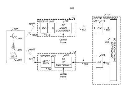
FIG. 1 is a diagram illustrating a transceiver 100 that may be used in
satellite
applications. The transceiver 100 includes a receive unit 102 communicatively
coupled
to a digital processing unit (DPU) 104 which is also communicatively coupled
to a
transmit unit 106.
The receiver unit 102 is coupled to a receive antenna 108 for sensing a
receive
signal 105R from another transceiver 100' such as a satellite 100A',
terrestrial
transceiver 100B', or a ground station 100C'. The sensed signal is amplified
by a low
noise amplifier (LNA) 110, and provided to a radio frequency (RF) down
converter 112.
CA 2995091 2018-02-13 3
The RF downconverter 112 downconverts the amplified signal from the LNA 110 in
frequency to a lower frequency (for example, L-band) signal 114. The
downconverted
signal 114 is digitally sampled and digitized by analog to digital (AID)
converter 116, and
the resulting digitized signal 118 is provided to a channelizer/digital
processor 120.
The digital channelizer 120 performs operations on the digitized downconverted
signal to generate a digital processed signal 122 that is converted to an
analog
processed signal 126 by digital-to-analog (D/A) converter 124. The analog
processed
signal is upconverted to higher frequency by RF upconverter 128, amplified by
amplifier
132 such as a traveling wave tube amplifier (TWTA) or solid state power
amplifier
(SSPA), and provided to the transmit antenna 134 to generate a transmit signal
105T to
one or more of the other transceivers 100'.
According to the well known Nyquist criteria, AID converter 116 must sample
the
downconverted signal at a rate at least twice the largest bandwidth of the
downconverted
signal itself to prevent aliasing. In practice, the sampling rate is even
higher, to account
for imperfect anti-aliasing filters which may induce phase distortion if the
frequency
cutoffs are too severe. Accordingly, the operations performed by the DPU 120
must
performed at a rate at least twice the largest bandwidth of the downconverted
signal 114.
DPUs 120 capable of processing signals at these high rates have been produced.
Such
DPUs 120 are expensive to design and produce. For typical satellite
applications, the
first signal 105 is a 500MHz L-band signal and the downconverted signal 114 is
n L-band
signal of 500 MHz bandwidth. Accordingly, DPUs 120 capable of processing
signals of
this bandwidth have been developed and are readily available.
As described above, other frequency bands have become available for such
communications, including Q-band (33-50Ghz), V-band (40-75 GHz) and W-band (75-
110 GHz). To use such wide bandwidths without incurring the expense of
developing
new DPUs capable of handling such bandwidths, the bandwidth must be reduced to
smaller (e.g. 500 MHz) chunks.
FIG. 2 is a diagram illustrating a modified transceiver 200. The transceiver
200
has been modified to include a plurality of receive units 102A-102N and a
plurality of
transmit units 106A-106N. Each receive unit 102-102N is responsible for
receiving a
different bandwidth portion of the receive signal 105RA-105RN, and providing a
500
MHz bandwidth signal in the L-band to the DPU 104. Each transmit unit 106A-
106N
4
Date Recue/Date Received 2021-07-22
accepts the 500 MHz, L band signal 126A-126N from the DPU 106 and generates
and
transmits an associated transmit signal 105TA-105TN on the appropriate portion
of the
spectrum.
The difficulty with the modified transceiver 200 illustrated in FIG. 5 is that
both the
.. receive units 102A-102N and the transmit units 106A-106N are expensive and
difficult to
produce. Since these devices must operate in millimeter frequency bands (for
example,
Q-band, V-band and W-band), these devices include waveguides of very small
size that
must be produced to very tight tolerances. Accordingly, while the modified
transceiver
200 can transceive signal on newly available frequency bands, this capability
comes at
great expense.
FIG. 3 is a diagram of an improved broadband transceiver 300. This improved
broadband transceiver (hereinafter simply referred to as transceiver 300)
comprises a
receive unit 302 and a transmit unit 306 that has been modified to transceive
signals at
higher frequency bands, as well as the digital processing unit 104 discussed
earlier with
respect to the baseline transceiver 100. Unlike the digital processing unit
104 in the
baseline transceiver 100 illustrated in FIG. 1, the digital processing unit
104 illustrated in
FIG. 3 is configured to process a plurality of signals (e.g. from
downconverters 316A-
316N). The transceiver 300 also includes a converter unit 304 that converts
the
downconverted signals from the receive unit 302 into signals to be processed
by the DPU
104 and also converts digitally processed signals from the DPU 104 into
signals to be
transmitted by the transmit unit 306. This transceiver 300 has the ability to
transceive
signals in the higher Q, V and W frequency bands, at lower cost compared to
the design
illustrated in FIG. 2, and is discussed below with reference to FIG. 4 and
FIGs. 5 and 6.
FIG. 4 is a diagram presenting exemplary operations that may be used to
receive
and process signals_ Referring to block 402, a first signal such as the
receive signal
305R depicted in FIG. 3 is received. This first signal 305R is in a first
frequency band
and of a first bandwidth, for example, a V band signal of 3GHz bandwidth. This
can be
accomplished, for example, by antenna 308 and LNA 310 of the receive unit 302.
In
block 404, the received first signal 305R is converted from the first
frequency band to a
first intermediate frequency band. This can be accomplished, for example, by
the RF
converter 312 of the receive unit, which converts the amplified version of the
received
signal V-band signal into an intermediate frequency band in the Ka-band, for
example.
5
Date Recue/Date Received 2020-05-14
In one embodiment, the intermediate frequency band that the received first
signal 305R
is converted into is determined such that its selection optimally minimizes
the
generation of spurs (described further below), and maximizes the reuse of
existing
hardware, which can be implemented by sharing hardware (e.g. one or more of
the
local oscillators 318 between the down converters 316 and upconverters 320).
In one
of the embodiments discussed below, an intermediate frequency band of 29.0-
32.0
GHz is chosen, because that intermediate frequency band provides an optimal
combination of spur minimization, reuse of existing downconverters 316, and
sharing of
local oscillators 318 between the downconverters 316 and the upconverters 320,
as
further described below.
Referring to block 406, the converted first signal (now in the intermediate
band)
is split into N intermediate signals, each in a respective one of a first set
of N sub-
bands, wherein In one embodiment, the number of intermediate signals N
is
chosen so that each of the N intermediate signals has a bandwidth equal to or
less than
the maximum bandwidth of a signal that can be processed by the DPU 104. For
example, if the DPU 104 is capable of processing 500 MHz signals, each of the
N
intermediate signals will be no greater than 500 MHz. If the received signal
is a 3 GHz
signal, it will be split into at least six (3/0.5) signals, each occupying a
different (and
optionally contiguous) sub-band of the 3GHz bandwidth signal. In the
illustrated
embodiment of FIG. 3, this operation is performed by splitter 314, which
splits the
intermediate band (Ka, in this example) signal from the RF down converter 312
into N
Ka band signals.
Next, in block 408, each of the N intermediate signals is downconverted into a
second frequency band. In the embodiment illustrated in FIG. 3, this is
accomplished
by N down converters 316A, each of which downconvert an associated signal from
the
splitter 314 from the associated one of the first set of N sub-bands of the
intermediate
frequency band (in the illustrated embodiment, the Ka band) to an associated
sub-band
of the second frequency band (in the illustrated embodiment, the L band). The
result is
N L-band sub-band signals, each of bandwidth equal to or less than the
bandwidth of
the receive signal 305R divided by N.
Each of the downconverters 316A-316N included in the converter unit 304 is
communicatively coupled with an associated one of a plurality of local
oscillators 318A-
318N. For example, downconverter 316A is communicatively coupled to local
oscillator
6
CA 2995091 2018-02-13
318A, and converter 316N is communicatively coupled to local oscillator 318N.
The
converters 316A-316N each receive a local oscillator signal from their
associated local
oscillator, and use that local oscillator signal in the downconversion
process.
The N downconverted intermediate signals are next processed with a digital
processor to generate N processed signals, as described in block 410 of FIG.4.
In the
embodiment depicted in FIG. 3, this is accomplished when each of the
downconverted
intermediate signals are provided to one or more AID converters 116, and the
resulting
digitized signals (of 500 MHz bandwidth each, in the illustrated embodiment)
are
provided to a channelizer/digital processor 120 for processing. The resulting
processed
signals are next provided to one or more D/A converters 124 to produce N
processed
digital signals.
In block 412, each of the N processed signals is upconverted to a respective
one
of a second set of N sub-bands in the second intermediate frequency band. In
the
exemplary embodiment presented in FIG. 3, this is accomplished by upconverters
320A-320N, with each of the upconverters 320A-320N upconverting one of the sub-
bands in the second frequency band (L-band in this illustrated embodiment) to
an
associated one of the sub-bands of the second intermediate frequency. We shall
note
that in the illustrated example in FIG. 3, the second intermediate frequency
band is
selected to be the same as the first intermediate frequency band; namely, Ka.
As noted above, each of the upconverters 320A-320N upconverts the associated
one of the signals in the N sub-bands of the second frequency band to an
associated
one of the second set of N sub-bands of the second intermediate frequency band
using
a local oscillator signal from an associated local oscillators. We shall note
that the local
oscillators associated with the up-convertors, 320A-320N, may or may not be
the same
local oscillators 318A-318N associated with the down-convertors 316A-316N. The
number of local oscillators required for the implementation of this system can
thus vary
depending on various optimization criteria. It can be 2N: one for each down-
convertor
316A-316N, and one for each up-convertor, 320A-320N. Or N local oscillators:
each
associated to a one down-convertors selected from 316A-316N and a one up-
convertor
selected from 320A-320N simultaneously. Or any other possible configuration.
Returning to FIG. 4, the upconverted signals are combined and the combined
upconverted signals are converted to a third frequency band, as shown in
blocks 413
and 414. This can be accomplished for example, by combining each of the
upconverted
7
CA 2995091 2018-02-13
signals (for example, with combiner 322), and providing the combined
upconverted
signals to the RE upconverter 328 of the transmit unit 306. The upconverter
328
upconverts the signals according to control inputs. Note that the third
frequency band
may or may not be the same as the first frequency band. In the illustrated
example of
FIG.5, the third band is selected to be the Q band spanning frequencies 37.5
to 40.5
GHz.
Finally, the converted signals are transmitted, as shown in block 416. This
can
be accomplished, for example, by providing the upconverted signal to an
amplifier 332
such as a traveling wave tube amplifier (TWTA) or solid state power amplifier
(SSPA),
and the amplified signal is provided to transmit antenna 334 for transmission
of the
transmit signal 305T.
As noted above, various optimization criteria can be used to select the first
and
the second intermediate frequency bands and the first and the second set of N
sub-
bands. For example, any or all of the N (Ka) sub-bands created by the splitter
314 can
be advantageously selected to be coextensive in frequency with the N (Ka) sub-
bands
combined by the combiner 322. This simplifies the design by requiring only N
local
oscillators 318 instead of 2N local oscillators, as they provide the same LO
signals for
the upconversion and downconversion process. In such embodiments, one or more
of
the local oscillators 318 and the local oscillator signals they produce are
shared by one
or more of the down converters 316 and associated up converters 320. For
example,
the local oscillator signal produced by local oscillator 318A (provided to
downconverter
316A for downconverting from a sub-band of the first set of N sub-bands to the
second
frequency band) may also be provided to the upconverter 320A for upconverting
the
processed signal to a sub-band of a second set of N sub-bands that is
coextensive in
frequency with the sub-band of the first set of sub-bands (for example, sub-
band 504A
is coextensive with sub-band 514A). The result is that fewer local oscillators
318 are
required.
This is made possible by selecting one or more of the first set of N sub-bands
used in the transmission (e.g. 504A-504F) to be coextensive in frequency with
an
associated sub-band of the second set of N sub-bands (514A-514F) used in
transmission. For example, any or all of the N intermediate signals may be
downconverted (e.g. by the associated one of the downconverters 316A-316N)
from a
Ka sub-band to the L band, and an associated one of the N processed signals
may be
8
CA 2995091 2018-02-13
upconverted (e.g. by the associated one of the upconverters 320A-320N) from
the L-
band to same (Ka) sub-band.
It is also noteworthy that the first intermediate frequency band (e.g.
frequency
band of the signal emanating from RF downconverter 312) need not be
coextensive
with the second frequency band (e.g. the frequency band of the signal provided
to the
RF upconverter 328). Instead, the first intermediate frequency band may
include only
some frequencies that overlap with those of the second intermediate frequency
band.
Even in such cases, one or more of the sub-bands of the first intermediate
frequency
can be chosen to be coextensive in frequency with an associated one or more of
the
sub-bands of the second intermediate frequency, thus providing for savings in
the
circuitry required to generate the local oscillator signals required to
perform the
upconversion and downconversion of the signals. Judicious selection of the
first
intermediate frequency band and second intermediate band, along with the first
and
second sets of N sub-bands in the respective first and second intermediate
bands
maximizes re-use of existing hardware, minimizes amount of additional elements
(e.g.
local oscillators 318) that are required, and minimizes the number of spurs
(as further
described below), while maintaining signal quality.
Although the greatest savings in the number of local oscillators 318 and
associated circuitry can be realized when every one of the first set of N sub-
bands used
in transmission (e.g. 504A-504F) is coextensive in frequency with the
associated one of
the second set of sub-bands (e.g. 514A-514F, respectively), savings can still
be
obtained when only one of the first set of sub-bands is selected to be
coextensive in
frequency with one of the second set of sub-bands. For example, the first set
of sub-
bands and second set of sub-bands may be chosen such that only two sub-bands
of
the first set of sub-bands is coextensive in frequency with an associated two
sub-bands
of the second set of sub-bands. Referring to FIG. 5, this may be accomplished
by
selecting sub-bands 504A and 504C to be coextensive in frequency with sub-
bands
514A and 514C, respectively, for further example.
FIG. 5 is a diagram illustrating an exemplary frequency plan for the broadband
transceiver 300. In this illustrated embodiment, the receive signal 305R is a
V-band
signal between 47.2 and 50.2 GHz. That signal may comprise a plurality of
contiguous
sub-bands 502A-502F as indicated in the diagram. That signal (following
reception and
low noise amplification) is downconverted (e.g. by downconverter 312 using
control
CA 2995091 2018-02-13 9
inputs) to a Ka band signal spanning 29.0-32.0 GHz, which may also be thought
of as
comprising a plurality of contiguous sub-bands 506A-506F. Those sub-bands 506A-
506F are separated into separate signals by splitter 314, and each such signal
is
provided to an associated downconverter 316A-316F. As illustrated, each of
such
signals has 500 MHz of bandwidth, and thus does not exceed the processing
capacity
of the DPU 104. Each of the signals is downconverted to an associated sub-band
of
the L-band before being provided to the DPU 104 for processing. Following such
processing, the processed signals are upconverted by upconverters 320A-320F.
Note
that although FIG. 5 illustrates an embodiment in which the the processed
signals are
upconverted to the same (e.g. frequency coextensive) Ka sub-bands that were
created
by splitter 314, the processed signals may be upconverted to different non-
coextensive
in frequency) sub-bands if desired. The upconverted signals are then combined
by
combiner 322, and converted from Ka-band to Q-band by converter 328. The
resulting
0-band signal spans the 37.5-40.5 GHz bandwidth, formed by 500 MHz sub-bands
516A-516F as illustrated in FIG. 5.
FIG. 5 also indicates which frequency allocations permit the re-use of
existing
hardware. Existing hardware operates in the Ka band from 27-31 GHz. However,
for
purposes of spur minimization and the use of same local oscillators for both
the
downconverters 316 and upconverters 320, it is desirable for the intermediate
frequency to extend from 29 GHz to 32 GHz. This permits re-use of existing
downconverters 316 for the 29-31GHz bands 506A-506D. Sub-bands that cannot be
implemented with re-used hardware are those indicated by forward-slashing, and
include sub bands disposed between 31.0 and 32.0 GHz.
Hence, as previously discussed, V-band sub-bands 502A-502F are new, and
.. require a different converter 312 than the converter 102 of FIG. 1 to
accommodate the
different frequency band and bandwidth. Downconverters 316A-316D for
downconverting signals to Ka sub-bands 506A-506D are used in existing
frequency
plans and do not require modification. Ka sub-bands 506E and 506F are not part
of a
current frequency plan, and minor modification of downconverters 316E-316F (as
indicated by forwardslashing) is required. Minor modifications are also
required of
upconverters 320A-320F. Converter 328 converts to the 0-band and hence
requires
significant modification, as indicated by back-slasing.
CA 2995091 2018-02-13
FIG. 6 is a diagram illustrating another exemplary frequency plan for the
transceiver 300. In this illustrated embodiment, the receive signal 305R is a
W-band
signal between 83.0 and 86.0 GHz. That signal may comprise a plurality of
contiguous
sub-bands 602A-602F as indicated in the diagram. That signal (following
reception and
low noise amplification) is downconverted (e.g. by downconverter 312 using
control
inputs) to a Ka band signal spanning 19.0-22.0 GHz, which may also be thought
of as
comprising a plurality of contiguous sub-bands 606A-606F. Those sub-bands 606A-
606F are separated into separate signals by splitter 314, and each such signal
is
provided to an associated downconverter 316A-316F. As illustrated, each of
such
signals has 500 MHz of bandwidth, and thus does not exceed the processing
capacity of
the DPU 104. Each of the signals is downconverted to an associated sub-band of
the L-
band before being provided to the DPU 104 for processing. Following such
processing,
the processed signals are upconverted by upconverters 320A-320F. Note that the
processed signals are upconverted to the same Ka sub-bands that were created
by
splitter 314. The upconverted signals are then combined by combiner 322, and
converted from Ka-band to V-band by converter 328. The resulting V-band signal
spans
the 71.0-74.0 GHz bandwidth, formed by 500 MHz sub-bands 616A-616F as
illustrated
in FIG. 6.
As was true with FIG. 5, FIG. 6 also indicates which frequency allocations
permit
the re-use of existing hardware. Existing hardware operates in the Ka band
from 27-31
GHz. However, for purposes of spur minimization and the use of same local
oscillators
for both the downconverters 316 and upconverters 320, it is desirable for the
intermediate frequency to extend from 19 GHz to 22 GHz. This permits re-use of
existing upconverters 320 for the 19-21GHz bands 612A-612D. Sub-bands that
cannot
be implemented with re-used hardware are those indicated by forward-slashing ,
and
include sub bands disposed between 31.0 and 32.0 GHz.
Hence, as previously discussed, the downconverters associated W-band sub-
bands 602A-602F cannot be reused from existing hardware, and require a
different
converter 312 than the converter 112 of FIG. Ito accommodate the different
frequency
band and bandwidth. Ka sub-bands 606A-606F are not part of a current frequency
plan,
and modification of downconverters 316A-316F (as indicated by forwardslashing)
is
required. Modifications are also required of upconverters 320E and 320F.
However,
11
Date Recue/Date Received 2021-07-22
upconverters 320A-320D for upconverting signals to Ka sub-bands 614A-614F are
used
in existing frequency plans and existing upconverters may be re-used.
Selected components of the transceiver 300 typically produce undesirable
harmonics and spurs that reduce transceiver 300 performance. For example,
downconverters 316A-316N operate by mixing the input signal with the local
oscillator
signal from the respective local oscillator 318A-318N. Ideally, this process
should simply
downconvert the signal content of the input signal to the desired frequency
band, but in
practice, non-linearities and other limitations of the hardware result in
harmonic distortion
that is comprised of signal components at harmonics of the input signal and
local
oscillator signal and their combination. Such harmonics are known as spurs.
The
frequency allocation plans described in FIG. 5 and FIG. 6 is the result of
optimizing the
selection of the intermediate frequency band (for example, the Ka band) and
the sub-
bands (for example the L sub-bands) minimize the generation of spurs in the
operating
bands of the transceiver 300. An example of such optimization will be detailed
below.
FIG. 7 is a diagram depicting the frequency of spurs generated in the V-Ka
band
downconversion process. Such spurs are the product of imperfections in the
mixing
process taking place in the downconverters. The spur frequency, and hence its
impact
to the desired performance depends on the input frequency provided to the
downconverter, the local oscillator frequency used by the downconverter, and
the
desired output frequency of the signal output by the downconverter.
The diagram depicted in FIG. 7 plots the frequency of the input (RF) signal on
the
vertical axis, the output frequency of spurs from the downconverter on the
horizontal axis
for a given local oscillator (LO) frequency (in the example illustrated in
FIG. 7, the LO
frequency is 9100 MHz, but others may be chosen). Each line on the plot is
labeled with
two numbers (m, n) wherein the first number (m) refers to a factor by which
the input
signal (input #1) frequency is multiplied, and the second number (n) refers to
a factor by
which the second input (input #2) frequency is multiplied. Further, the order
of the "spur"
is determined as the sum of absolute value of m and the absolute value of n.
The
shaded box in FIG. 7 represents the input frequencies to the RF downconverter
312 in
.. the frequency plan illustrated in FIG. 5, namely from 47,200 MHz to 50,200
MHz, and the
desired output IF frequencies of 29,000 MHz to 32,000 MHz.
With regard to the (1,-2) line, the value "1" refers to the fundamental of the
input
signal and the value "-2" refers to the 2nd harmonic of the LO input of 9100
MHz. Since
12
Date Recue/Date Received 2021-07-22
the converter 312 uses a harmonic mixer and uses the 2nd harmonic of the LO
input as
the effective LO. Hence, the line labeled (1, -2) reflects the desired output
mix product
of the downconverter 312 and is not regarded as a spur to be avoided. The
other lines
presented on FIG. 7 refer to potential spurs.
Spurs and other distortions may be reduced or ameliorated by appropriate
filtering by frequency (e.g. low pass, high pass, or bandpass filters). At the
same time,
it is not possible to construct filters with perfect bandpass characteristics,
and filters with
steep cutoff slopes typically induce phase distortions that may be seen in the
frequencies also occupied by signal content. Accordingly, it is desirable that
any high
power spurs are to be located at frequencies farther from the passband, so
that they
may be more easily filtered out without introducing phase distortion. Such
high power
spurs are indicated in the diagram of FIG. 7 by those lines having a low
Iml+Inl
numbers or also know as spur order. Conversely, lines having lower numbers
(e.g.
those where m is zero) represent spurs that are difficult to remove by
filtering, and are
preferably avoided. What constitutes lower order spurs depends upon the
application
to which the system is to be used. For purposes of communication in the
frequency
regimes discussed in this application, it is preferable to avoid spurs of
order 5 or less
(e.g.lml+Inl 5).
In the illustrated case, the first input is the RF signal in the V-band and
the
second input is the from the local oscillator, which is set to 9100 MHz. The
potential
frequency location of spurs is determined by following a horizontal line from
the input
frequency to the diagonal lines, and reading the frequency of the potential
spur on the x
axis. Therefore, to determine the frequency of the third order spur defined by
(0,3), a
horizontal line is drawn from input#1 to the (0,3) line. This indicates the
potential
presence of a spur at about 27,500 MHz for all input#1 frequencies. This
frequency is
well out of the desired output band from 29,000-32,000 MHz, and hence not a
problem.
Similarly, the frequency of the fourth order spur defined by (0,4) is
determined by
a horizontal line from input#1 to the (0,4) line, which shows a potential spur
at about
36,400 Hz for all input #1 frequencies. Hence, the shaded area illustrated in
FIG. 7
avoids the vertical lines (0, 3) and (0,4) and includes only higher order (>5)
spurs.
Accordingly, the use of the second harmonic of an local oscillator frequency
of 9100
MHz to mix the 47,200-50,200 MHz frequency range down to 29,000-32,000 MHz
range is a suitable choice.
CA 2995091 2018-02-13 13
The foregoing analysis can also be performed with respect to the
downconversion process performed by downconverters 316A-316N, the upconversion
process performed by upconverters 320A-320N, and the upconversion process
performed by upconverter 328.
FIGs. 8A-8E illustrate the generation of spurs in the downconversion process,
as
performed by downconverters 316A-316F. FIG. 8A presents a plot of spur
generation
by downconverter 316A in the frequency plan illustrated in FIG. 5, while FIGs.
8B-8F
present plots of spur generation by respective downconverters 316B-316F in the
frequency plan illustrated in FIG. 5. Note that in each case presented, the
generated
spurs do not include any fundamentals (0, n), and comprise mostly higher order
spurs
that can be readily filtered. The forward-slashed boxes represent an analysis
of the
spurs potentially generated by each down converter 316, while the back-slashed
boxes
represent an analysis of the spurs potentially generated by the other
downconverters
316 of the transceiver.
FIGs. 9A-9E illustrate the generation of spurs in the upconversion process, as
performed by upconverters 320A-320F. FIG. 9A presents an plot of spur
generation by
downconverter 316A in the frequency plan illustrated in FIG. 5, while FIGs. 9B-
9F
present plots of spur generation by respective downconverters 320B-320F in the
frequency plan illustrated in FIG. 5. Note again that in each case presented,
the
generated spurs avoid any fundamentals (0, n), and comprise mostly higher
order spurs
that can be readily filtered. The forward slashed boxes represent an analysis
of the
spurs potentially generated by each up converter 320, while the back-slashed
boxes
represent an analysis of the spurs potentially generated by the other
upconverters 320
of the transceiver.
FIG. 10 illustrates the generation of spurs in the upconversion process, as
performed by upconverter 328. Note again that in each case presented, the
generated
spurs avoid any fundamentals (0, n), and comprise mostly higher order spurs
that can
be readily filtered.
As can be seen from the plots presented in FIG. 7, FIGs. 8A-8F, FIGs. 9A-9F,
and FIG. 10, although the downconverters 316A-316F and the upconverters 320A-
320F
each generate harmonics, judicious choice of the characteristics of the N sub-
bands
(e.g. in terms of center frequency and/or bandwidth) before downconversion and
after
downconversion can result in a system that substantially excludes spurs from
key
14
CA 2995091 2018-02-13
frequency bands. In this context, "substantial" exclusion of the spurs does
not
necessarily require that all spurs be excluded. Instead, this requires that
the amplitude
and/or phase of any remaining spurs be such that their appearance in frequency
bands
of interest does not negatively affect the performance of the transceiver 100
to a
degree that the transceiver's functionality is unacceptably compromised for
its intended
use. When the spurs are far enough away from the band these spur can be then
filtered
by suitable means. The key spurs that are evaluated are the (0, n) spurs also
known as
LO harmonic spurs, the (1,n) spurs, and spurs that have a spur order ( also
known as
Iml+Ini value for a given (m,n) spur) less than or equal to 5.
Hardware Environment
FIG. 11 is a diagram illustrating an exemplary digital processing unit 104
having a
channelizer/digital processor (hereinafter signal processor 120) that could be
used to
implement processing elements of the above disclosure.
The signal processor 120 comprises a processor 1102, communicatively coupled
to a memory 1104 storing instructions for performing the operations discussed
above.
The processor 1102 may comprise a general purpose 1102A processor and/or a
special
purpose processor 1102B. For example, the special purpose processor 1102B may
be
implemented in one or more application specific integrated circuits (ASICs)or
field
programmable gate arrays (FPGAs), which may be implemented on the same or
different structure as the other elements of the signal processor 120. The
memory 1104
may include random access memory (RAM) 1104A and/or read only memory (ROM)
1104B, which for example, may include programmable read only memory (PROMs).
The signal processor 120 accepts input RF signals from A/Ds 116 and using the
processor 1102 and instructions stored in memory 1104, generates output
signals based
on the input signals and provides the resulting output signals to D/As 124. In
one
embodiment, the output signals are also generated in accordance with
configuration
commands and/or externally provided data. The output signals and/or
intermediate data
generated in the process of generating the output signals may be provided via
telemetry.
In the illustrated embodiment, the signal processor 120 may include a number
of
modules including a demodulator 1108, modulator 1106, pre-distortion
compensation
Date Recue/Date Received 2021-07-22
module 1110, switch router module 1112, and an encryption and/or decryption
module
1114. The demodulator module 1108 demodulates the input signal from A/Ds 116
for
further processing. The signal pre-distortion compensation module modifies the
input
signal according to an inverse model the gain and phase characteristics of the
signal
processor 120. This introduces "inverse distortion" into the process such that
the
resulting output signals are linearized. Switch router module 1112 routes
input signals
to other modules or processors and similarly routes output signals to the
appropriate
output. Encrypt/Decrypt module 1114 decrypts incoming signals and encrypts
output
signals as required. Any or all of module 1106-1114 may be implemented by use
of
processor 1102 instructions stored in the memory 1104, or may be implemented
as
separate hardware or firmware modules, using appropriate circuitry and/or
ancillary
processors and memory as appropriate.
Of course, those skilled in the art will recognize that any combination of the
above components and functionalities, or any number of different components
and
functionalities may be integrated into the signal processor 120.
25
CA 2995091 2018-02-13 16