Note: Descriptions are shown in the official language in which they were submitted.
CA 02995131 2018-02-08
WO 2016/026055 PCT/CA2015/050808
LC MODULATOR DEVICES BASED ON NON-UNIFORM ELECTRODE
STRUCTURES
Technical Field
[001] The invention relates generally to liquid crystal modulator optical
devices and
more specifically to shutters and smart windows, and methods for manufacturing
thereof.
Background
[002] Light modulation devices have many applications in photonics
(telecommunication, imaging, energy conservation, etc.). The modulation may be
activated by means of various mechanisms based on: mechanical movement,
deformation, photochromism, charged particle motion, electro optic modulation
in
interferential or polarimetric schemes and finally by using electrically
controllable light
transmission.
[003] The last approach is particularly interesting for shutter (imaging),
energy saving
(so called "smart windows"), privacy (image destroying) and color control
applications.
In addition, electrically controllable systems that are operated without
polarizers are
gaining in cost reduction, energy efficiency and reliability.
[004] One of the traditional methods of obtaining electro optic modulation of
light
transmission is based on the use of Polymer Dispersed Liquid Crystals (PDLCs),
as
described in Doane, Chien, Yang and Bos chapters 1, 4, 5, 11, 12, 13 of
"Liquid
Crystals in Complex Geometries", edited by GP Crawford & S. Zumer (Taylor &
Frances, London. 1996). With reference to Figures 1A and 1B, such materials
are
typically composed from 25% of liquid crystal dispersed (in the form of
droplets) into a
solid polymer matrix (75%). While being efficient for privacy window
applications, there
are however several drawbacks with this approach: most important of them being
that
the light scattering provided is dominantly forward scattering and thus is not
very
efficient for energy flux control. Another drawback is the presence of the
polymer
matrix of the PDLC which contributes to yellowing of such a modulated pane,
when
1
CA 02995131 2018-02-08
WO 2016/026055 PCT/CA2015/050808
used for example as a window exposed to sunlight. The high operating voltages
and
the angular dependent scattering (haze) are other significant drawbacks.
[005] Electric modulation of light was demonstrated also in so called Polymer
Stabilized Liquid Crystal (PSLC) compounds by R. A. M. Hikmet in "Electrically
Induced
Light Scattering from Anisotropic Gels", J. Appl. Phys. 68, pp. 4406, 1990,
where the
polymer content is significantly reduced, typically to 5%, while the remaining
mass
(95%) is composed of liquid crystal. Figure 2 shows an example of such a
structure
with a polymer concentration gradient, going from almost 100% of liquid
crystal (right
bottom corner) to almost 100% of polymer (left top corner), T. Galstian,
"Liquid Crystals,
Polymers, and Electrically Tunable Optical Components", 19 April 2010, SPIE
Newsroom.
[006] The light scattering may be controlled by the appropriate choice of
material
parameters. For example, in L. Komitov, L-C. Chien, S. H. Kim, "Method of
Fabricating
Electro-Optical Devices with Polymer Stabilized Liquid Crystal", US patent
8,081,272,
Dec. 20, 2011 and M. Mitov, N. Dessaud, "Cholesteric Liquid Crystalline
Materials
Reflecting more than 50% of Unpolarized Incident Light Intensity", Liq. Cryst.
34, no. 2,
pp. 183-193, 2007, cholesteric (or "helical") liquid crystal material was used
in the
above mentioned PSLC configuration to obtain preferential back scattering of
light.
While the back scattering is increased compared to the use of simple, so
called
"nematic", liquid crystals, the main problem of photo chemical stability
(yellowing in
sunlight) remains. However, it is difficult to eliminate the polymer content
since its
presence is an important factor particularly for obtaining modulators of high
efficiency.
[007] Natural light may be presented as the sum of two orthogonal
polarizations (two
crossed linear polarizations or two opposed circular polarizations). The use
of
cholesteric liquid crystal material typically ensures the reflection (or back
scattering) of
only (mainly) one circular polarization, while the opposed circular
polarization is not
affected by the material. That is why, various "polymer matrix programming"
methods
have been developed to provide the reflection of both types of circular
polarizations,
see M. Mitov, N. Dessaud, "Cholesteric Liquid Crystalline Materials Reflecting
more
2
CA 02995131 2018-02-08
WO 2016/026055 PCT/CA2015/050808
than 50% of Unpolarized Incident Light Intensity", Liq. Cryst. 34, no. 2, pp.
183-193,
2007.
[008] Further efforts were devoted by J.-P. Bedard-Arcand, T. Galstian in
,"Self
Organization of Liquid-Crystal and Reactive-Mesogen into 2D Surface Stabilized
Structures," Macromolecules, 44, 344-348, 2011, to the development of light
modulators with less volumetric polymer content, by creating so called Surface
Polymer
Stabilized Liquid Crystal (S-PSLC) material systems. However, the complexity
of
manufacturing: mixing the liquid crystal with a polymerizable monomer
composition, its
handling, dispersion, polymerization, stability, etc. still remain a problem.
[009] In some applications, such as for windows, providing a controllable
reflection of
50% of incident light is practical to reduce the amount of light entering a
window, even if
control over substantially 100% of the light could be preferable. Being able
to switch
from reflection to transmission (either with diffusion or with transparency,
or both), is
desirable. Cholesteric Liquid Crystal (CLC) materials provide the ability to
reflect light,
however, the electric field strength required to change the state of the
liquid crystal to
remove the reflection can be nearly prohibitive.
Summary
[0010] Applicant has discovered that the helically ordered state of CLC
materials that
provides reflection can be changed to be more transmissive under favorable
conditions
of electric field strength by using non-uniform electric fields instead of
uniform electric
fields. Electric field lines that are not perpendicular to the planes of the
substrates
containing the CLC material help change the helical structure of the CLC
towards a
homeotropic structure using lower field strengths than for electric field
lines that are
perpendicular. For example and without limitation, control voltages can be
lowered
from over 100V to less than 10V for cells of similar properties.
[0011] Applicant has discovered that uniform electric fields can be applied
following a
non-uniform electric field to complete a transition and/or maintain a
transmissive state
3
CA 02995131 2018-02-08
WO 2016/026055 PCT/CA2015/050808
of the CLC material. Electrode structures for providing non-uniform and
uniform electric
fields are disclosed herein.
[0012] Applicant has discovered that dual frequency CLC materials can be
controlled to
change from a reflective state to a transmissive state at one frequency and
from a
transmissive state back to a reflective state at another frequency.
[0013] Liquid crystal modulator optical devices, and more specifically
shutters and smart
windows, are presented along with their methods of manufacture. Shutters can
reflect
light and/or cause light to be diffused, like a frosted window, in which case
they are also
called "privacy windows". Smart windows typically control energy flow,
although color
temperature control for windows and variable lighting devices or light
projectors are also
applications. The liquid crystal modulator devices are characterized by
reduced polymer
content in the material composition of the liquid crystal layer and
characterized by non-
uniform electrode structures in the LC structure configured to generate
spatially non-
uniform electric fields and therefore non-uniform molecular reorientation of
LC
molecules. This arrangement provides electrically controllable light
scattering.
[0014] In accordance with one aspect of the proposed solution there is
provided a liquid
crystal modulator for modulating incident light, the modulator comprising:
first and
second polymeric layers providing electrical isolation; first and second
transparent
electrode layers sandwiching said first and second polymeric layers
therebetween, at
least one of said transparent electrodes being non-uniform and a remaining
transparent
electrode being uniform; and Liquid Crystal (LC) material sandwiched between a
said
polymeric layers, said liquid crystal material having a non-uniform LC
molecular director
orientation.
[0015] In accordance with another aspect of the proposed solution there is
provided a
modulator wherein said first and second layers (for example, polymeric layers)
are
preferably rub-free, said first electrode is non-uniform, said second
electrode is uniform,
said LC material is cholesteric LC material, said modulator further
comprising: a third
4
CA 02995131 2018-02-08
WO 2016/026055
PCT/CA2015/050808
uniform electrode outside said first electrode and a transparent isolation
layer between
said first and second electrodes.
[0018] In accordance with a further aspect of the proposed solution there is
provided a
liquid crystal modulator for modulating incident light, the modulator
preferably
comprising: first and second layers (for example, polymeric layers) providing
alignment
and/or electrical isolation; first and second transparent electrode layers
sandwiching
said first and second layers therebetween, at least one of said transparent
electrodes
being non-uniform and a remaining transparent electrode being uniform; and
Liquid
Crystal (LC) material sandwiched between said layers, said liquid crystal
material
having a non-uniform LC molecular director orientation, wherein said LC
material is a
cholesteric LC material of a first helicity and said LC layer comprises a
polymeric matrix
set in the presence of said cholesteric LC material of a second opposite
helicity.
[0017] In accordance with yet another aspect of the proposed solution there is
provided
a modulator further comprising a temperature gradient structure providing a
chirp in the
pitch of the helical structure of said cholesteric LC material. Also, the cell
may be filled
by a "dual frequency" cholesteric liquid crystal.
[0018] In accordance with yet another aspect of the proposed solution there is
provided
a method of driving the liquid crystal modulator where a sequence of
electrical
excitation is applied to transit from uniform reflecting state into non
uniform scattering
state with the help of non-uniform electrodes and using relatively low driving
voltages;
followed by the application of voltage between two outer electrodes to obtain
finally a
uniform transparent state.
[0019] In accordance with yet another aspect of the proposed solution there is
provided
a liquid crystal modulator with non-uniform reorientation state that can
increase lights
divergence and be maintained by a train of pulses and used as privacy window
(destroying the image quality of transmitted light).
[0020] In accordance with yet another aspect of the proposed solution there is
provided
a liquid crystal modulator with non-uniform electrode layer that contains
multiple
CA 02995131 2018-02-08
WO 2016/026055 PCT/CA2015/050808
independent electrodes which may be controlled by multiple electrical signals
with
different amplitudes, phases or frequencies.
[0021] In accordance with yet another aspect of the proposed solution there is
provided
a liquid crystal modulator with multiple liquid crystal cells having different
helicitities to
reflect the orthogonal polarization components of the incident light as well
as different
resonant reflection wavelengths to provide more spectral independent control.
Brief Description of the Drawings
[0022] The proposed solution will be better understood by way of the following
detailed
description of embodiments with reference to the appended drawings, in which:
[0023] Figure 'IA and 113 are schematic diagrams illustrating a prior art
material
respectively scattering and transmitting light;
[0024] Figure 2 is an illustration of a prior art polymer concentration
gradient in a liquid
crystal;
[0025] Figure 3 is a schematic diagram illustrating a layered geometry of a
liquid crystal
cell in accordance with an implementation of a first embodiment of the
proposed
solution;
[0026] Figure 4 is a schematic diagram illustrating a layered geometry of a
liquid crystal
cell in accordance with another implementation of the first embodiment of the
proposed
solution;
[0027] Figure 5 is a schematic diagram illustrating a layered geometry of a
liquid crystal
cell in accordance with a further implementation of the first embodiment of
the proposed
solution;
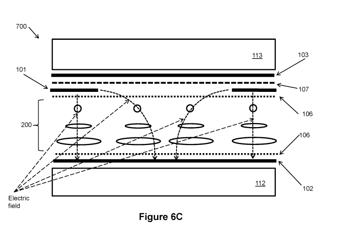
[0028] Figure 6A is a schematic diagram illustrating a layered geometry of a
liquid
crystal cell in accordance with another embodiment of the proposed solution;
6
CA 02995131 2018-02-08
WO 2016/026055 PCT/CA2015/050808
[0029] Figure 68 is another schematic diagram illustrating a layered geometry
of a liquid
crystal cell in accordance with another implementation of the second
embodiment of the
proposed solution;
[0030] Figure 6C is a further schematic diagram illustrating a micro scale
layered
geometry of a liquid crystal cell in accordance with a further implementation
of the
second embodiment of the proposed solution;
[0031] Figure 7 is a further schematic diagram illustrating a large scale
layered
geometry of a liquid crystal cell in accordance with the implementation of the
second
embodiment of the proposed solution illustrated in Figure 6C;
[0032] Figures 8A, 8B, 8C and 8D are schematic diagrams illustrating different
LC
orientational states in accordance with the third implementation of the second
embodiment of the proposed solution;
[0033] Figure 9A is a schematic diagram illustrating an optical shutter in
accordance
with the proposed solution;
[0034] Figure 9B is a schematic diagram illustrating a color control device in
accordance
with the proposed solution;
[0035] Figure 10 is a schematic diagram illustrating a privacy window/diffuser
in
accordance with the proposed solution;
[0036] Figure 11 is a schematic diagram illustrating a controllable reflector
plate in
accordance with the proposed solution;
[0037] Figure 12 is a schematic diagram illustrating wafer scale manufacturing
employing mask deposition techniques in accordance with the proposed solution;
[0038] Figure 13 is a schematic diagram illustrating a liquid crystal
modulator device in
the form of a greenhouse window pane in a transparent state in accordance an
embodiment of the proposed solution;
7
CA 02995131 2018-02-08
WO 2016/026055 PCT/CA2015/050808
[0039] Figure 14 is a schematic diagram illustrating a liquid crystal
modulator device in
the form of a greenhouse window pane in a reflecting state in accordance the
embodiment of the proposed solution;
[0040] Figure 15 is a plot of the resonance of binary cholesteric LC mixtures
versus
composition;
[0041] Figure 16 is a plot illustrating a temperature dependence of the
resonant
wavelength of reflection;
[0042] Figure 17 is a schematic diagram illustrating high temperature
resonance at
shorter wavelengths to reflect sunlight in accordance with the proposed
solution;
[0043] Figure 18 is a schematic diagram illustrating low temperature resonance
at
longer wavelengths to reflect infra red radiation in accordance with the
proposed
solution;
[0044] Figure 19 is a schematic diagram illustrating wavelength conversion in
a window
pane in accordance with the proposed solution;
[0045] Figure 20A is a plot illustrating the variance of the cholesteric
resonance of MDA-
02-3211 with temperature;
[0046] Figure 20B is another plot illustrating the variance of the cholesteric
resonance of
cholesteric compounds;
[0047] Figure 21 is a plot illustrating the variance of the resonance
wavelength with
chiral dopant concentration;
[0048] Figure 22A is a schematic diagram illustrating interferential coatings
cancelling
back reflection irrespective of the presence of a non-uniform layer in
accordance with
the proposed solution;
[0049] Figure 22B is a schematic diagram illustrating interferential coatings
canceling
back reflection by employing a hiding layer in accordance with the proposed
solution;
8
CA 02995131 2018-02-08
WO 2016/026055 PCT/CA2015/050808
[0050] Figure 23 is an illustration of an example of a non-uniform electrode
pattern in
accordance with the proposed solution;
[0051] Figure 24 is a transmission plot illustrating electrical control of
transmission
spectra in accordance with the proposed solution;
[0052] Figure 25 is a schematic diagram illustrating a high modulation depth
layered
structure in accordance with the proposed solution; and
[0053] Figure 26 is a schematic diagram illustrating a reflection bandwidth
broadening
layered structure in accordance with the proposed solution,
[0054] wherein similar features bear similar labels throughout the drawings.
While the
layer sequence described is of significance, reference in the present
specification to
qualifiers such as "top" and "bottom" is made solely with reference to the
orientation of
the drawings as presented in the application and do not imply any absolute
spatial
orientation.
Detailed Descri pti on
[0055] In accordance with one embodiment of the proposed solution, polymer
content is
substantially removed from the material composition of an LC layer itself and
a non-
uniform electrode structure is employed configured to generate a spatially non-
uniform
molecular reorientation of the liquid crystal material to scatter light in an
electrically
controllable manner.
[0056]Figure 3 illustrates an implementation 300 in which a nematic LC layer
100
substantially free of polymer is preferably sandwiched between a pair of LC
orientation
layers 105 (e.g. organic polymer or inorganic layers) which provide electrical
isolation
and induce a preferential orientation of LC molecular directors in the LC
material 100.
Alternatively, the transparent electrode layers 101 and/or 102 can be used to
align the
liquid crystal 100, for example by rubbing the transparent electrode material.
An electric
9
CA 02995131 2018-02-08
WO 2016/026055 PCT/CA2015/050808
field is applied to the LC layer 100 via a uniform transparent electrode 102
(e.g. Indium
Tin Oxide (ITO)) and a non-uniform transparent electrode 101 (e.g. ITO)
sandwiching
the LC layer 100 outside the LC orientation layers 105. An optional index
matching
layer (not shown) can be employed in combination with the transparent
electrodes.
Optionally, the non-uniform transparent electrode 101 may be patterned (holes,
lines,
etc.) and controlled by one electric potential. Alternatively, multiple
independent
electrode patterns may be used and controlled by more than one voltage.
[0057] While the polymer network of a PSLC or the droplet character of liquid
crystals in
PDLCs guarantee a rapid return to a ground state when the electric field is
reduced, in
accordance with another implementation of the proposed solution dual frequency
nematic liquid crystals (100) are employed to provide such a response (De
Gennes
P.G. and Prost J., "The Physics of Liquid Crystals", Oxford University Press,
1995, 2nd
Edition). Dual frequency nematic LC materials (100) can be forced to relax by
changing
the frequency of the electric field. In accordance with a third
implementation, dual
frequency cholesteric liquid crystals (100) are employed which, in addition,
would
provide control of energy flux by providing back reflection/scattering of
light.
[0058] However, the above proposed solutions suffer from polarization
dependence.
When using simple nematic liquid crystal compositions in the absence of
polarizers
what is needed to obtain a polarization independent operation is the
generation of three
dimensional (3D) orientation defects (of liquid crystal molecules) in the LC
layer 100.
The generation of 3D orientation defects can be achieved in different ways:
[0059] In accordance with a fourth implementation, planar unidirectional
orientation
layers 105 are employed to define strong alignment boundary conditions in the
ground
state, together with non-uniform transparent electrodes 101 (as described
hereinabove)
on each side of the LC layer 100 sandwiched therebetween. This can be achieved
by
the use of two non-uniform electrodes 101 as described above (with one or more
control voltages) on each side of the LC layer 100, preferably, spatially
shifted and
cross-oriented in a layered geometry 400 schematically illustrated in the
Figure 4. A
particular example of an electrode structure includes chaotically distributed
holes on the
- _
CA 02995131 2018-02-08
WO 2016/026055 PCT/CA2015/050808
surfaces of both transparent electrodes 101. Another example is the use of
linear strip
electrodes on each substrate 101 (the geometrical pattern of strip electrodes
can vary
as desired), however if the orientation of the stripes of one electrode 101 on
one
substrate 111 is, say along X axis, then the orientation of the stripes of the
other
electrode 101 on the opposed substrate 111 is along the Y axis (Z axis being
perpendicular to the cell substrates). Another example is illustrated in
Figure 23 which
is a micro photograph of an example of spatially non-uniform ITO electrode.
[0060] In accordance with a fifth implementation, polarization independence
can be
achieved by using two alignment layers 105 oriented in perpendicular
directions,
generating a twisted alignment of the nematic liquid crystal material 100 in
the ground
state, for example as shown in the layered geometry 500 illustrated in Figure
5. Both
electrode layers can be non-uniform 101 or a combination of uniform electrode
layer
102 and non-uniform electrode layer 101 can be used.
[0061] In accordance with a sixth implementation of the proposed solution, a
similar
effect of reducing polarization dependence of light scattering can be obtained
by
employing cholesteric liquid crystal (single or dual frequency) materials
(200) of given
helicity. In this implementation, electrically induced orientation defects can
be made
such that one of the circularly polarized components of the incident light is
back
reflected and/or scattered by the first layers of the LC material (200) (with
the given
circularity), while the "non-affected" circular polarization of light is
gradually depolarized
during its propagation in the initial layers of the LC material (200) and then
is gradually
reflected from the remaining layers of the material (still with the same
circularity).
[0062] In manufacturing layered geometries in accordance with the above
embodiment,
the first (top) support substrate 111 is covered by a non-uniform, e.g. "hole-
patterned",
transparent conductive electrode 101 (which can also be patterned and
controlled by
multiple voltages and different frequencies and phases), such as ITO. The non-
uniform
hole patterning can be manufactured, for example, by local laser exposition
(deposition
/ ablation / etching) or by chemical etching. Typical hole sizes can be, for
example, in
the order of 5 to 30 micrometers and the distances between holes can be
between, for
11
CA 02995131 2018-02-08
WO 2016/026055 PCT/CA2015/050808
example, 3 to 15 micrometers. The holes can be distributed on the substrate
111
surface as periodic, quasi periodic, chirped or preferably as chaotic 2D
arrays, such that
the electric potential applied to conductive layer 101 propagates over the
connected
surface. This substrate 101 is preferably also covered by a unidirectionally
rubbed
layer of polyimide 105. The second bottom substrate 112 is covered by a
uniform
transparent and conductive layer 102, for example including an ITO electrode
102
preferably (but not necessisarily) coated with a rubbed polyimide layer 105.
The
thickness of the LC cell can be between 5 to 20 micrometers. Preferably, the
LC cell is
filled with dual-frequency cholesteric liquid crystal 200 for example having a
reflection
resonance in the visible spectrum.
[0063] In the operation of the dual frequency cholesteric liquid crystal
implementation, a
spectrally resonant reflection of light of given circularity is provided in
the absence of
electrical excitation as the liquid crystal molecules 200 align uniformly due
to the
presence of the alignment layers 105. This ground state can, in principle, be
different
depending if the LC cell 300/400/500 was relaxed after excitation for example
at 1 kHz
(positive liquid crystal dielectric anisotropy) or after excitation for
example at 100 kHz
(negative liquid crystal dielectric anisotropy). The defect structure in the
excited state
will be different for the case of excitation with 1 kHz frequency that is
destroying the
helix by "attracting" molecular axes to the electric field, compared to
excitation at 100
kHz that is "repulsing" the liquid crystal molecules away from the electric
field.
[0064] However, from a manufacturing point of view, it would be desirable to
make
liquid crystal cell-sandwiches 600 without alignment layers (105) (alignment
layers
which are usually obtained by rubbing, oblique deposition in vacuum or. photo
exposition). In addition, the removal of the alignment step and, for example
by using
low anchoring energy materials 106 or simply omitting the rubbing step can
help induce
orientation defects in the ground state, between the excitation states, when
there is no
electrical excitation in the un-powered state as illustrated in Figure 6A.
However, such
defects are difficult to reproduce on a manufacturing scale and, once obtained
are not
stable against mechanical deformations or temperature variations.
12
Yr. .011000.10.0110111110..,
CA 02995131 2018-02-08
WO 2016/026055
PCT/CA2015/050808
[00651 In accordance with another embodiment of the proposed solution, liquid
crystal
sandwiches as previously described are employed however without inducing a
preferential alignment direction. In order to address the above mentioned
problems of
control and instability, the use (during operation) of a sequence of
electrical pulses or a
train of pulses is proposed to maintain the LC cell state in the desired
"defect"
configuration, which can be clusterized and thus non-uniform or uniform such
as in a
reflecting helix configuration.
[0066] In accordance with another implementation of the previous embodiment,
liquid
crystal sandwiches (300/400/500) as previously described are used without
inducing a
preferential alignment direction, however to address the above mentioned
problems of
control and instability, an additional layer 103 of transparent conductive
electrode
(optionally with an index matching layer) is employed as shown in the layered
geometry
700 illustrated in Figure 66. The role of the electrically isolating layer 107
may be
important since, in this implementation, different zones of the non-uniform
ITO are
needed to have the same or similar electrical potential, while at the same
time a
significantly different potential is needed uniformly to cover the holes of
the non-uniform
electrode 101. The different portions (lines, etc.) of the non-uniform
electrode 101 may
be controlled by using different voltages, phases and frequencies.
[0067] The use of two uniform electrodes 102 (in "traditional" devices)
provides an
electric field which is perpendicular to the substrates to unwind a uniform
helix of CLC,
which requires a relatively high threshold voltage to start the process.
Employing the
proposed non-uniform electrode 101 (/103) approach provides low voltage level
operation to unwind the uniform Cholesteric Liquid Crystal (CLC) helix (in
fact, it would
even start without threshold). This is demonstrated schematically in Figure 6C
for one
"hole" (or one "pair") of ITO by the perpendicular (on both peripheries) and
tilted
(internal sides of holes) electric fields.
The presence of ITO non-uniformities
correspondingly creates non-uniformities in the electrical field.
[0068] In accordance with the above embodiment, the "natural" alignment of the
liquid
crystal material can contain molecular alignment defects which will scatter
light,
13
Atrowoompow
CA 02995131 2018-02-08
WO 2016/026055 PCT/CA2015/050808
including scattering in the back direction, providing energy flux control. The
application
of a voltage between the uniform electrodes 103 & 102 can stabilize the
helical
structure if the frequency of the electrical signal is, for example, 100 kHz
as illustrated in
Figure 7. In this case, the cell 700 selectively reflects 50% light of given
wavelength
and circular polarization. There are many techniques, including the use of a
second cell
(700) with the liquid crystal material 200 of opposed chirality (other
handedness), to
achieve additional reflection up to 100%. In the case in which the frequency
of an
applied electrical voltage is switched for example to 1 kHz, then the electric
field
destroys the helical structure of the liquid crystal 200 and orients molecules
in the
perpendicular direction to the substrates 112/113. In this state (Figure 8D)
the cell
becomes substantially transparent for all wavelengths, polarizations and
propagation
directions (without haze).
[0069] The proposed device 700 has much more operational variability since a
voltage
can further be applied between the electrodes 101 & 102, which creates
different types
of defects due to the non-uniformity of the electrode 101 depending upon the
frequency
of the electrical field applied. The defects can be formed by the attraction
of molecular
axes if the frequency is for example 1 kHz and by the repulsion of molecular
axes if the
frequency is for example 100 kHz. It has been discovered that the ground state
orientation when the field is removed will have different defects depending on
the
original state, excited by 1 kHz or 100 kHz. This step of application of
voltage between
electrodes 101 and 102 may be used as an intermediate step when passing from
reflective to transmissive states to reduce the voltage required to unwind the
helix. In
this case, this step may be followed by the application of a low frequency
voltage
between two uniform electrodes 102 & 103.
[0070] With reference to Figures 8A, 8B, 8C and 8D the above described modes
of
operation are characterized by:
(0071] Figure 8A illustrates the state corresponding to the application of
electrical
potential difference U applied at a high frequency, eg. 100 kHz, between
electrodes 103
& 102, with the electrode 101 being left (electrically) floating, potential
difference which
14
CA 02995131 2018-02-08
WO 2016/026055 PCT/CA2015/050808
stabilizes a uniform helical structure of LC 200 reflecting 50% of natural
light with 'a
resonant wavelength. Figure 88 illustrates the state corresponding to the
potential
difference U applied at a low frequency, e.g. 1 kHz, between electrodes 101 &
102, with
electrode 103 being left (electrically) floating which destroys the helical
structure and
creates orientation defects or positive micro lenses assuming that the optical
anisotropy
An of the LC 200 is positive (divergent micro lenses can be obtained if the
optical
anisotropy of the LC 200 is negative). Figure 8C illustrates the state
corresponding to
the potential U applied at a high frequency between the electrodes 101 & 102,
with
electrode 103 being left (electrically) floating which creates chaotically
oriented helical
clusters and thus scatters light. Figure 80 illustrates the state
corresponding to the
potential difference U applied at a low frequency between the uniform
electrodes 102 &
103 with the non-uniform electrode 101 left (electrically) floating which
creates uniform
molecular orientation (homeotropic) that is substantially optically
transparent.
Intermediate defect states, which can be obtained when relaxing from
excitation states,
are also possible and very useful (not shown). To enable all the above
mentioned
independent control states, the electrical isolation layer 107 between the
electrodes 101
& 103 must be efficient enough, which can be controlled by the choice of its
thickness d
and dielectric constant c, to eliminate capacitive coupling between the two
electrode
layers 101 & 103. Otherwise, the presence of the uniform electrode 103 may
uniformize the electrical potential be applied to the electrode layer 101
inhibiting the
creation of defects. (It will be understood that additional optional index
matching
layeres are not shown.)
[0072] The same structure 700 may be filled by a standard liquid crystal,
including, for
example, homeotropically aligned (in the ground or unpowered state) nematic
liquid
crystals 100. In this case case, the non-uniform electrode layer 101 (with or
without the
help of the opposed uniform electrode 102) may be used to create various non-
uniform
molecular configurations, e.g., to focus, broaded or steer light. In
"traditional" devices,
to go back to the original transmission (e.g., without steering) the field is
removed and
the natural relaxation brings the system back to the homeotropic state. This
may be
long, for example for near infra red steering (scanning) applications.
However, in the
CA 02995131 2018-02-08
WO 2016/026055 PCT/CA2015/050808
proposed device the presence of two uniform electrodes 102 / 103 can help to
quickly
bring the liquid crystal molecules 100/200 back to their background
homeotropic
alignment. Then the system will remain in this state ready to steer again.
Other
unpowered (ground state) orientations also may be considered here.
[0073] In addition to spectral control over reflection, it is possible to
provide spectral
control over absorption. The cholesteric LC 200 (normal or preferentially dual
frequency) is doped by dichroic dopants (dyes: e.g., blue anthraquinone,
azobenzene,
carbon nanotubes, etc.) which are aligned with the local director of the LC
200. In this
case, their total absorption (averaged along the depth of the LC cell) will be
different
compared to the case when the helix is unwound and the LC is homeotropically
aligned
(which will thus realign also the dichroic dopants). The resonant wavelength
of
reflection of the helix ARR may be chosen to be the same as the resonant
absorption
wavelength ARA of the dichroic dopant. In this case, the switch will enable
the overall
transmission control at Ao = ARR = ARA. In contrast, if ARR ARA, then the
switch (between
helical and homeotropic states) will enable the simultaneous control of the
resonant
reflection and absorption of the guest-host material system. More
sophisticated control
depending on whether the dischroism of the dopant is positive or negative can
be
obtained. In one interesting case, the ARA may be in the infra-red spectral
region to
control the energy flow through a window containing the device(s) described
herein.
[0074] The ability to modulate a color of light transmitted can thus be
enhanced by
using a dichroic dopant, such as dyes or carbon nanotubes that align with the
liquid
crystal 200 (100) to provide high absorption in a specific spectral range.
While the
resonant reflection spectra of the cholesteric helix, namely the host, may be
in the same
or in another, e.g. visible, spectra. In the planar state of cholesteric
cells, the reflection
and absorption are predetermined. Once a low frequency voltage is applied to
such
cells (700), they are transformed into homeotropic state, and the resonant
reflection
disappears, and the absorption also changes. This arrangement can be used to
change
the color temperature of an LED light source, for example. (An example
implementation
is presented in Figure 96 in which an LED can be used in a flash device for a
variable
visible or near infrared illuminator.) In this case, both the ARA and ARR may
be in the
16
CA 02995131 2018-02-08
WO 2016/026055
PCT/CA2015/050808
visible spectral band (still different, ARA # ARR ) and the switch will allow
better control
over the spectra of the transmitted light. For example, if the helical state
reflects in the
red band and the dye has a positive dichroic absorption in the green band,
then the
helical state would correspond to the reflection of the red and higher
absorption of the
green, and thus, for white incident light, the transmitted light will be
mainly blue. The
switch to the homeotropic state will eliminate the red reflection and also
will reduce the
green absorption and the transmitted light will look more as white. It will
also be
appreciated that multiple cholesteric cells 700 with different resonant
wavelengths (pitch
of helix) can be combined with different absorption wavelengths (dichroic
dyes).
[0075] This provides a very rich set of possible orientational configurations:
[0076] - defect texture in the ground state at no voltage following relaxation
.from 1 kHz
excitation state,
[0077] - defect texture supported by a train of pulses at low frequency,
[0078] - defect texture in the ground state at no voltage following relaxation
from 100
kHz excitation state,
[0079] - defect texture in excited state at 1 kHz with electrical potential
difference
applied between electrodes 102 and 101,
[0080] - defect texture in excited state at 100 kHz with electrical potential
difference
applied between electrodes 102 and 101,
[0081] - uniform helicoidal texture with resonant reflection in excited state
at 100 kHz
with electrical potential difference applied between electrodes 102 and 103,
[0082] - uniform helical texture that is unpowered thanks to the surface
alignment (105),
[0083] - uniform homeotropic texture (substantially transparent) in excited
state at 1 kHz
with electrical potential difference applied between electrodes 102 and 103,
as well as
17
CA 02995131 2018-02-08
WO 2016/026055
PCT/CA2015/050808
[0084] - other stable, quasi-stable or bistable defect structures by applying
specific
transitory electrical excitation signals (sequences of different voltages and
frequencies)
between different electrode pairs.
[0085] The proposed Liquid Crystal Modulator (LCM) devices can be used as:
[0086] - light shutters or variable diaphragms, for example for optical
imaging (Figure
9A);
[0087] - mobile variable illumination (divergence, color, etc.) in the visible
spectrum (for
example for imaging) or in the near infrared spectrum, for example for eye
scanning,
etc. (Figure 9B),
[0088] - for controlling light scattering in forward propagation direction for
example to
controllably destroy the transmitted image for privacy windows, (Figure 10);
[0089] - for partially controlling the color of transmitted light;
[0090] - for diffusing point sources of light for example to soften LED
lighting and/or to
control its glare (Figure 10);
[0091] - for controlling energy flow by controllable light reflection, for
example in "energy
smart" buildings (Figure 11); etc.
[0092] Manufacturing includes (Figure 12): the top substrate 113 is first
covered by a
uniform transparent conductive electrode 103, such as ITO which is then
covered with a
relatively thick (several micrometers + or -) isolation layer 107 that can be
dielectric,
metal oxides, etc., and then covered by a "hole-patterned" ITO electrode 101.
Without
limiting the invention, the hole patterned electrode 101 can be obtained from
a uniform
electrode, for example by chemical etching (Figure 23). The typical size of
holes or
electrode spacing can be in the order of 5 micrometers and the distances
between
holes could be between 10 to 20 micrometers, the non-uniformities being
distributed on
the surface as periodic, quasi periodic or preferably chaotic 2D arrays. This
layered
structure can also be covered by an electrically and orientationally isolating
layer for
18
__________________________________ 41111101.11MONimisimmwelaw.
CA 02995131 2018-02-08
WO 2016/026055 PCT/CA2015/050808
example a layer of polyimide 106, however without rubbing. The second bottom
substrate 112 can have an ITO electrode 102 thereon and can be covered by an
isolating layer, such as a non-rubbed polyimide 106. The LC cell 700 is filled
with a
dual frequency cholesteric liquid crystal 200, preferably with a resonance in
the visible
range. The thickness of the LC cell 700 can be between 5 to 20 micrometers.
[0093] The proposed devices can be manufactured by using techniques of large
scale
processing developed for example by the liquid crystal display industry.
Depending
upon the target application, the layered structure of the LC cell (700) and
the complexity
of the electrical driving scheme can be different. For example, thin film
transistors can
be added if the device is used for imaging applications. At the opposite end
of the
manufacturing spectrum, the layered structure of the LC cell (700) and the
driving
scheme can be extremely simple if the device is used as smart window.
[0094] The manufacturing approach can also be adapted to enable flexible and
customized manufacturing. For example, the arrangement of various layers and
the
mask deposition can be used as illustrated in the Figure 12 wherein the dashed
lines
schematically show possible dicing lines providing custom sizing. In this
case, the
dicing process can be performed at low temperature (followed by additional
sealing by
adhesive) or with a laser, etc. and the parts thus separated can provide
access to
various electrode layers. Alternatively, conductive adhesive or other type of
electrode
points can be positioned at various positions to enable electrical contact
from the side
edge or through-hole connections can be used to obtain the required post-
fabrication
customization of large panels.
[0095]The proposed Liquid Crystal Modulator (LCM) devices can be used also as
window panes providing an artificially "enhanced greenhouse effect". The
classical
greenhouse effect consists of transmitting one incoming wavelength (typically
short)
and blocking (absorbing) other predetermined typically longer wavelengths
which are
emitted by internal objects as outgoing radiation. Incorporating helical LC
molecular
structures (200) with known spectrally resonant reflection, the proposed
multitask
windows can be set to be transparent (Figure 13) for a certain period of time
(e.g.,
19
CA 02995131 2018-02-08
WO 2016/026055
PCT/CA2015/050808
during the day) to allow energy flow into the greenhouse; and then switched to
their
helical resonantly reflecting state to prohibit the energy from going out
during the night
(Figure 14) wherein the composition of the LC material layer (or one of
layers) is
chosen to reflect resonantly the specific wavelength (within a band) emitted
by the
internal objects (plants). Thus the rate of radiative heat evacuation may be
controlled.
[0096] Figure 24 illustrates an example of electrical control of transmission
spectra in a
cholesteric liquid crystal cell 300/500/700 having a uniform 102 and a non-
uniform 101
ITO layers. The cholesteric resonance is strongest between (in a band) 510nm
and
580nm which is back reflected for a control field of below 20V. If used for
window pane
applications this represents a significant reduction in the visible Sun
spectrum. The
cholesteric helix is destroyed at voltages above 20V. The back scattering is
very high
for 34V which results in low transmission and the transmission increases when
the
applied voltage is high ¨ uniformizing alignment. It is noted that the
transmission
spectra correspond to a single controlled temperature and chiral composition.
The
above LCM devices employ active control which can be enabled in various ways,
including for example a photo voltaic source.
[0097] The resonant character of the LC material 200 can be employed to
provide Self-
Adjusting LCMs (SA-LCM) which is possible because the resonance wavelength of
the
LC materials 200 is sensitive to concentrations as illustrated in Figure 15,
(De Gennes
P.G. and Prost J., "The Physics of Liquid Crystals", Oxford University Press,
1995, 2nd
Edition) and to various natural stimuli, such as the temperature as
illustrated in Figure
16, (V.A. Beliakov, A. S. Sonin, "Optics of Cholesteric Liquid Crystals",
Nauka, 1982) for
(1) cholesterol perlargonat, (2) cholesterol caprinat and (3) the same as (1)
but in a
narrow temperature range (see right vertical axes).
[0098] Therefore LC material 200 composition can be configured to exhibit the
resonant
(reflecting or back scattering) state which corresponds to low transmission
conditions in
a given temperature range in order to reflect light falling thereon as
illustrated in Figure
17, while with decrease in temperature (when, for example, the temperature of
internal
objects and air become lower), the resonant wavelength of the LC mixture 200
is shifted
4111111111111110.11.111.1k.
CA 02995131 2018-02-08
WO 2016/026055
PCT/CA2015/050808
and light transmission of the SA-LCM becomes higher as illustrated in Figure
18. For
example, the temperature dependence of the LC material 200 composition of the
SA-
LCM can be used to adjust the LCM in a way to have high reflectivity and back
scattering at high temperatures to limit the energy penetration into the
building, say at
green wavelengths (resonance range), while a reduction in temperature would
shift the
resonant wavelength zone into the infra red range to reflect light coming from
the
interior to preserve the energy in the room. The effect is reversible and self-
adjusting.
[0099] In still another embodiment light sensitive dyes can be added which can
absorb
light and introduce a specific shift of the resonance either by creating
temperature
changes or by transforming themselves (such as, for example, trans to cis
isomerization) which will then shift the resonance spectral position of the
cholesteric LC
200 used. Both of the proposed liquid crystal modulator devices (LCM and SA-
LCM)
can be used in conjunction with wavelength conversion elements (dyes, metal or
other
nano particles, etc.) to also increase the efficiency of the wavelength
conversion of light
for energy control, agricultural and photo voltaic applications. Namely, the
energy
conversion is done during the crossing (by light) of a given thickness of the
host (LC)
material where the above mentioned elements are introduced their (pane)
fabrication. If
the host (LC) material 200 is composed (entirely or partially) from above
mentioned
helical structures, then certain wavelengths of light (in a range/band) can
have higher
efficient trajectories in the (LC) material 200 because of multiple
reflections from the
helical structures as illustrated in Figure 19. For example Figure 20A
illustrates
temperature dependence of the cholesteric resonance of (LC material 200) MDA-
02-
3211, and for other cholesteric compounds in Figure 20B.
[00100] Figure 21 illustrates the variance of the resonance
wavelength with chiral
dopant concentration.
[00101] In the above, reference has been made to "index
matched layers". By
index matched layers, for example in the case of patterned transparent
electrodes 101
(such as IT0s) or in the case of the isolating layer 107/106 (such as Si02),
the
following can be included:
21
=
CA 02995131 2018-02-08
WO 2016/026055 PCT/CA2015/050808
[00102] - The
uniform layer 102 / 103 in question is coated on several
dielectric layers and additional dielectric layers are coated on the top of
the layer. The
thicknesses and refractive indexes of those dielectric layers are chosen in a
way to
"interferentially" cancel the back reflection of light from the layer and
ultimately from the
entire stack of coated layers.
[00103] - The
non-uniform layer 101 in question is coated as described
above, but additional dielectric layers are configured and coated in a way
that the
interferential cancelling of the back reflection is achieved on different
areas of the non-
uniform layer irrespective of the presence of the non-uniform layer for
example as
illustrated in Figure 22A.
[00104] - The
non-uniform layer 101 in question is coated on the substrate directly
on several dielectric layers, but the refractive index of the non-uniform
layer is chosen in
a way to "hide" its non-uniformities by the next layer (coated on the
immediate top of the
non-uniform layer) having the same refractive index. Further dielectric layers
can be
coated on the top of the "hiding" layer to improve the efficiency by
interferential
cancelling for example as illustrated in Figure 22B.
[00105] In
applications which require high modulation depths, double liquid crystal
layers 200 with opposed circularity can be employed. The simplest layered
geometry
could include two similar layer sandwiches 700 which contain two LC layers 200
of
opposed (circularity) helicicity attached together. Such layered construction
provides
an improvement in providing low voltage driven modulators (shutters, windows,
etc.).
However, there is no need to duplicate the structure 700 of Figure 7. Only one
"combined" non-uniform electrode layer 101 (with or without index matching)
can be
employed in a layered geometry 800 to simplify the manufacturing process and
save
cost, as is illustrated in the Figure 25.
[00106] This
type of device (with a single intermediate electrode, or just
duplicating the basic structure and attaching two similar sandwiches 700) can
be further
improved by broadening the reflection resonance, shown in the Figure 24. Some
22
CA 02995131 2018-02-08
WO 2016/026055 PCT/CA2015/050808
applications, such as shutter for imaging devices, would require a specific
operation
mode: transparent or reflecting (preferably without forward scattering) in a
relatively
broad spectral band (for example, ideally between 400nm to 700nm or at least
between
450nm to 650nm). One way of providing such band broadening employs in the LC
material layer one helicity cholesteric (say "right") and a monomer
polymerized to form
a specific polymer network, then removing the cholesteric material and filling
the
polymer network with cholesteric LC of opposed helicity (see works by M.
Mitov, N.
Tabiryan, etc.)
[00107] As another technique of broadening is the use of spatially varying
periodicity of the helix by providing a gradient in the polymer network.
Broadening of
the reflection resonance can include for example (referring to Figure 16)
providing a
temperature gradient as illustrated in Figure 26 to create a chirp in the
pitch of the
helical structure (200), which in turn can broaden the reflection resonance.
[00108] Accordingly, LC modulators are proposed which are based on electric
field generation of refractive index modulation defects without using polymer
networks
(PDLCs, PSLCs or S-PSLCs, etc.) or complex surface relief formation.
[00109] In accordance with yet another embodiment of the proposed solution,
a
split LC cell layered structure can be manufactured by inserting a broadband
birefringent layer (such as a stretched Polyimide) configured to provide a
half wave
plate into one simple sandwich LC cell layered structure of a given
cholesteric LC
material 200 described hereinabove. The birefringent layer has two opposed
surfaces
configured to align cholesteric LC material 200 of the same circularity on
either side
thereof in the planar direction. For certainty, it is not necessary for the
alignment on the
opposed sides of the birefringent layer to be parallel to one another; uniform
alignment
on each side would suffice.
[00110] The principle of operation of such a layered structure causes the
first front
cholesteric LC layer to reflect 50% of incident natural light (namely 100% of
circularly
polarized light of one circularity/helicity/handedness), the remaining 50% of
light the
23
- -- -
CA 02995131 2018-02-08
WO 2016/026055 PCT/CA2015/050808
incident natural light (namely 100% of the remaining circularly polarized
light of the
opposed circularity) is transformed into the opposed circularity as it
propagates through
the second birefringent layer (the half wave plate). The incident light having
passed
through the half wave plate birefringement layer is then reflected by the
second back
layer of cholesteric LC material (of the same helicity as the first
cholesteric LC layer).
The light reflected by the back cholesteric LC layer is transformed again into
the original
circularity by propagating through the half wave plate birefringent layer a
second time,
and then passes substantially unchanged through the first front cholesteric LC
layer.
[00111] In accordance with some implementations, the birefringent layer
(substrate) can be covered with an ITO layer for heating the central layer
region (part)
of this split LC cell (as illustrated in Figure 26) creating a gradient of
temperature and a
corresponding pitch of the helix of the cholesteric LC. The temperature
gradient
broadens the reflection spectra from a typical 50nm preferably up to 150nm, to
cover a
wavelength range, for example from 400nm to 650nm. Such a layered structure
900
can provide a shutter for miniature cameras (for example by unwinding the
helix
structures as descried hereinabove). For certainty, the birefringent layer is
not limited
to a half wave retarder plate, the birefringent layer can be configured to
retard an odd
number of half waves.
[00112] While the invention has been shown and described with reference to
preferred embodiments thereof, it will be recognized by those skilled in the
art that
various changes in form and detail may be made therein without departing from
the
spirit and scope of the invention as defined by the appended claims.
24