Note: Descriptions are shown in the official language in which they were submitted.
CA 02995607 2018-02-13
WO 2017/049030 PCT/US2016/052049
1
SEMICONDUCTOR PACKAGE WITH EMBEDDED DIE
AND MANUFACTURING METHOD THEREOF
Field of Disclosure
[0001] The field of the disclosed subject matter generally relates to
semiconductor devices
and to methods of manufacturing the semiconductor devices. In particular, the
field
of the disclosed subject matter relates to embedding of one or more dies in a
substrate
of a semiconductor device.
Background
[0002] In a conventional die embedding process, a cavity is first made in a
dielectric. Then a
die is inserted in the cavity. This is followed by laminating the dielectric
and the
metal layer. However, the conventional process requires more processes and
materials like cavity forming, attaching film for die placement, and detaching
the
film. Also, it has die dislocation problems. Further, the die and the metal
layer can
be misaligned.
SUMMARY
[0003] This summary identifies features of some example aspects, and is not an
exclusive or
exhaustive description of the disclosed subject matter. Whether features or
aspects
are included in, or omitted from this Summary is not intended as indicative of
relative importance of such features. Additional features and aspects are
described,
and will become apparent to persons skilled in the art upon reading the
following
detailed description and viewing the drawings that form a part thereof
[0004] An exemplary semiconductor device is disclosed. The semiconductor
device may
comprise a substrate, a first die, first die bumps, first joints and patterned
contacts.
The first die may be embedded in the substrate. The first die bumps may be
coupled
to the first die, and the first joints may be coupled to the first die bumps.
The
patterned contacts may be coupled to the first joints such that the first die
is
electrically coupled to the patterned contacts through the first die bumps and
the first
joints. The patterned contacts may be at or below a height of the substrate.
[0005] An exemplary method of manufacturing a semiconductor device is
disclosed. The
method may comprise forming a first die. The method may also comprise forming
CA 02995607 2018-02-13
WO 2017/049030 PCT/US2016/052049
2
first die bumps and coupling the first die bumps to the first die. The method
may
further comprise forming first joints and coupling the first joints to the
first die
bumps. The method may further comprise forming patterned contacts and coupling
the patterned contacts to the first joints such that the first die is
electrically coupled to
the patterned contacts through the first die bumps and the first joints. The
method
may further comprise providing a substrate such that the first die is embedded
in the
substrate and such that the patterned contacts are at or below a height of the
substrate.
[0006] Another exemplary method of manufacturing a semiconductor device is
disclosed.
The method may comprise forming a carrier. The method may also comprise
forming a first die assembly on the carrier. The method may further comprise
separating the first die assembly from the carrier. The process of forming the
first die
assembly may comprise forming patterned contacts on the carrier. The process
may
also comprise forming a first die. The process may further comprise forming
first die
bumps and coupling the first die bumps to the first die. The process may
further
comprise forming first joints and coupling the first joints to the first die
bumps and to
the patterned contacts such that the first die is electrically coupled to the
patterned
contacts through the first die bumps and the first joints. The process may
further
comprise providing a substrate such that the first die is embedded in the
substrate and
such that the patterned contacts are at or below a height of the substrate.
BRIEF DESCRIPTION OF THE DRAWINGS
[0007] The accompanying drawings are presented to aid in the description of
embodiments
of one or more aspects of the disclosed subject matter and are provided solely
for
illustration of the embodiments and not limitation thereof
[0008] FIG. 1A illustrates an example embodiment of a semiconductor device;
[0009] FIG. 1B illustrates another example embodiment of a semiconductor
device;
[0010] FIGs. 2A and 2B illustrate examples of different stages of forming a
semiconductor
device;
[0011] FIGs. 2C ¨ 2F illustrate examples of different stages of forming a
semiconductor
device of FIG. 1A;
[0012] FIGs. 2G ¨ 2J illustrate examples of different stages of forming a
semiconductor
device of FIG. 1B;
CA 02995607 2018-02-13
WO 2017/049030 PCT/US2016/052049
3
[0013] FIG. 3 illustrates a flow chart of an example method of forming a
semiconductor
device;
[0014] FIG. 4 illustrates a flow chart of another example method of forming a
semiconductor device;
[0015] FIG. 5 illustrates a flow chart of an example process of forming a die
assembly; and
[0016] FIG. 6 illustrates examples of devices with a die assembly integrated
therein.
DETAILED DESCRIPTION
[0017] Aspects of the subject matter are provided in the following description
and related
drawings directed to specific embodiments of the disclosed subject matter.
Alternate
embodiments may be devised without departing from the scope of the disclosed
subject matter. Additionally, well-known elements will not be described in
detail or
will be omitted so as not to obscure the relevant details.
[0018] The word "exemplary" is used herein to mean "serving as an example,
instance, or
illustration." Any embodiment described herein as "exemplary" is not
necessarily to
be construed as preferred or advantageous over other embodiments. Likewise,
the
term "embodiments" does not require that all embodiments of the disclosed
subject
matter include the discussed feature, advantage or mode of operation.
[0019] The terminology used herein is for the purpose of describing particular
embodiments
only and is not intended to be limiting of embodiments of the disclosed
subject
matter. As used herein, the singular forms "a", "an" and "the" are intended to
include
the plural forms as well, unless the context clearly indicates otherwise. It
will be
further understood that the terms "comprises", "comprising,", "includes"
and/or
"including", when used herein, specify the presence of stated features,
integers,
processes, operations, elements, and/or components, but do not preclude the
presence
or addition of one or more other features, integers, processes, operations,
elements,
components, and/or groups thereof
[0020] Further, many embodiments are described in terms of sequences of
actions to be
performed by, for example, elements of a computing device. It will be
recognized
that various actions described herein can be performed by specific circuits
(e.g.,
application specific integrated circuits (ASICs)), by program instructions
being
executed by one or more processors, or by a combination of both. Additionally,
these
CA 02995607 2018-02-13
WO 2017/049030 PCT/US2016/052049
4
sequence of actions described herein can be considered to be embodied entirely
within any form of computer readable storage medium having stored therein a
corresponding set of computer instructions that upon execution would cause an
associated processor to perform the functionality described herein. Thus, the
various
aspects may be embodied in a number of different forms, all of which have been
contemplated to be within the scope of the claimed subject matter. In
addition, for
each of the embodiments described herein, the corresponding form of any such
embodiments may be described herein as, for example, "logic configured to"
perform
the described action.
[0021] As indicated above, conventional die embedding processes typically
include making
a cavity in a dielectric, inserting the die into the cavity, followed by
laminating the
dielectric and the metal layer. Also as indicated above, such conventional die
embedding processes can cause the die to dislocate and/or the metal layer to
be
misaligned.
[0022] However, in an aspect, it is proposed to mount a die on an already made
circuit
pattern. This can be accomplished through a die attaching process such as mass
reflow or thermal compression bonding. Thereafter, substrate (e.g.,
dielectric) and
other metal layers can be laminated. This has at least the following
advantages.
First, there is no need to form a cavity for die placement. Thus, activities
such as
cavity forming, tape laminating to place and hold the die in cavity, and tape
detaching
typical of the conventional process are no longer required. Second, the die
dislocation and misalignment between the die and metal pattern associated with
the
conventional process can be prevented. Third, finer pitch bump connections are
possible.
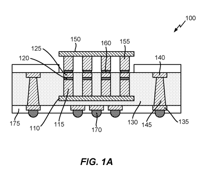
[0023] FIG. 1A illustrates an example embodiment of a semiconductor device
according to
an aspect of the disclosed subject matter. The semiconductor device in FIG. 1A
may
be formed through one or more methods that will be described in detail further
below. The semiconductor device may include a substrate 130, which may be
formed of an insulator and/or a dielectric material. The semiconductor device
may
also include a first die 110, first die bumps 115 (e.g. interconnects,
pillars, copper
pillars) and first joints 120 (e.g. solder joint or other material which
allows the first
die bumps 115 to be coupled to another conductor). The first die 110, which
may
CA 02995607 2018-02-13
WO 2017/049030 PCT/US2016/052049
comprise a logic circuit and/or a memory circuit or other type of die, may be
embedded in the substrate 130. The first die bumps 115 may provide electrical
connections to the first die 110 ¨ more specifically, may provide connections
to the
circuit of the first die 110. The first die bumps 115 may be formed from
conductive
materials such as copper. The first joints 120 may be coupled to the first die
bumps
115.
[0024] The semiconductor device may include patterned contacts 125 formed on
the first
joints 120. The patterned contacts 125 may be coupled to the first joints 120
such
that the first die 110 can be electrically coupled to the patterned contacts
125 through
the first die bumps 115 and the first joints 120. The patterned contacts 125
may be at
or below a height of the substrate 130. In FIG. 1A, the patterned contacts 125
are
illustrated as being within the substrate 130 and coplanar with a top surface
of the
substrate 130, i.e., at the height of the substrate 130.
[0025] FIG. 1B illustrates another example embodiment of a semiconductor
device
according to an aspect of the disclosed subject matter. The semiconductor
device of
FIG. 1B is similar to that of FIG. 1A. However, the devices differ in the
following
respect. The device in FIG. 1B may include an underfill 180 disposed at least
partially around the patterned contacts 125, the first die bumps 115, and the
first
joints 120. The device in FIG. 1B may be formed with an underfill process
(e.g. the
underfill 180) while the device in FIG. 1A may be formed without the underfill
process.
[0026] As seen in both FIGs. 1A and 1B, the semiconductor device may
optionally include a
second die 150, second die bumps 155 and second joints 160. The second die 150
may comprise a logic circuit and/or a memory circuit. The second die bumps 155
may provide electrical connections to the second die 150 ¨ more specifically
provide
connections to the circuit of the second die 150. The second die bumps 155 may
be
formed from conductive materials such as copper.
[0027] The second joints 160, which may also be solder joints or other
conductive material,
may be coupled to the second die bumps 155 and to the patterned contacts 125.
For
example, the second joints 160 may be coupled to the second die bumps 155 on
one
side and coupled to the patterned contacts 125 on another side such that the
first die
110 can be electrically coupled to the second die 150 through the first die
bumps 115,
CA 02995607 2018-02-13
WO 2017/049030 PCT/US2016/052049
6
the first joints 120, the patterned contacts 125, the second joints 160 and
the second
die bumps 155.
[0028] Unlike the first die 110, at least a portion of the second die 150 may
be at or above
the height of the substrate 130. In FIGs. 1A and 1B, the second die 150 in its
entirety
is illustrated as being above the substrate 130. When the patterned contacts
125 are
coplanar with the top surface of the substrate 130, then the second die bumps
155 and
second joints 160 may also be at or above the height of the substrate.
[0029] The semiconductor device may include resist layers 175 (e.g., solder
resist layers)
formed above and/or below the substrate 130. The device may also include one
or
more first conductive layers 135 formed at a first surface (e.g., lower
surface) of the
substrate 130 within the lower resist layer 175. The first conductive layers
135,
which may represent traces, may be formed from conductive materials such as
copper.
[0030] The semiconductor device may include one or more second conductive
layers 140
formed within the substrate 130. In FIGs. 1A and 1B, the second conductive
layers
140 are shown to be formed at a second surface (e.g., upper surface) of the
substrate
130. That is, the second conductive layers 140 may be coplanar with the
patterned
contacts 125. While not shown in these figures, the second conductive layers
140
may represent traces. Some of these traces may electrically couple with the
circuit of
the first die 110 and/or the second die 150.
[0031] The semiconductor device may include one or more vias 145. Through-
substrate vias
(TSVs) are one examples of vias 145. The vias 145 may electrically couple the
first
conductive layers 135 to the second conductive layers 140. The vias 145 may be
formed from a conductive material such as copper.
[0032] The semiconductor device may include one or more third bumps 170
coupled to the
first conductive layers 135. The third bumps 170 may be formed as solder
bumps.
External access to the semiconductor device (e.g., to the first die 110 and/or
the
second die 150) may be provided through the third bumps 170. That is,
electrical
coupling of external devices with the first and/or second die 110, 150 may be
provided through the third bumps 170, the first conductive layers 135, the
vias 145
and the second conductive layers 140.
CA 02995607 2018-02-13
WO 2017/049030 PCT/US2016/052049
7
[0033] FIGs. 2A ¨ 2J illustrates different processing stages of forming a
semiconductor
device. FIGs. 2A and 2B illustrate examples of stages common to forming the
semiconductor devices of both FIGs. 1A and 1B. FIGs. 2C ¨ 2F illustrate
examples
of stages of forming the semiconductor device of FIG. 1A. FIGs. 2G ¨ 2J
illustrate
examples of stages of forming the semiconductor device of FIG. 1B.
[0034] As seen in these figures, there can be a carrier 205 on which a
semiconductor device
may be formed. In particular, a die assembly, which includes a die, can be
formed on
either side of the carrier 205. For convenience of description, the die
assembly
formed on a lower side of the carrier 205 will be described. The die assembly
formed
below the carrier 205 will be referred to as the first die assembly 290 and
will be
assumed to include the first die 110.
[0035] Note that a similar assembly may be formed an upper side the carrier
205 and can just
as easily be used. Also, the two assemblies ¨ above and below the carrier 205
¨ may
be formed together as illustrated in the figures. If the upper assembly is
also formed,
then much of the discussion related to the first die assembly 290 may apply to
the
upper assembly unless indicated otherwise. It should be noted that terms such
as
"upper" and "lower" are used for convenience, and should not be taken to refer
to
absolute directions unless indicated otherwise.
[0036] FIG. 2A illustrates a stage in forming a semiconductor device, and in
particular a
stage in forming the first die assembly 290. As seen, the patterned contacts
125 and
the second conductive layers 140 may be formed on the carrier 205. In doing
so, the
patterned contacts 125 and the second conductive layer 140 can be made to be
coplanar.
[0037] FIG. 2B illustrates a stage in forming the first die assembly 290 in
which the first die
110, the first die bumps 115 and the first joints 120 may be formed. The first
die
bumps 115 may be formed to couple to the first die 110. Also, the first joints
120
may be formed to couple to the first die bumps 115 (e.g., on one side) and to
the
patterned contacts 125 (e.g., on another side). In this way, the first die 110
may be
electrically coupled to the patterned contacts 125 through the first die bumps
115 and
the first joints 120.
[0038] FIG. 2C illustrates a stage of forming the first die assembly 290 in
which the
substrate 130 may be provided. As seen, the substrate 130 may be provided so
as to
CA 02995607 2018-02-13
WO 2017/049030 PCT/US2016/052049
8
embed the first die 110 in the substrate 130. For example, the substrate 130
may be
provided on the carrier 205 and grown (downwards in the figure) so as to
partially or
completely encapsulate the first die 110. The substrate 130 may also be
provided
such that the patterned contacts 125 are at or below the height of the
substrate 130.
In this particular example, the patterned contacts 125 and the substrate 130
are shown
to be at the same height. In an embodiment, this can be accomplished without a
polishing process since both the patterned contacts 125 and the substrate 130
can be
formed on the carrier 205.
[0039] In an aspect, the substrate 130 may be provided after the first die
110, the first die
bumps 115, the first joints 120, and the patterned contacts 125 are formed.
That is,
the stage illustrated in FIG. 2C can be subsequent to the stages illustrated
in FIGs. 2A
and 2B. By providing the substrate 130 subsequently, the first die 110 can be
embedded in the substrate 130 without having to form a cavity.
[0040] FIG. 2C corresponds to a stage of forming the semiconductor device
illustrated in
FIG. 1A in which the substrate 130 may be disposed at least partially around
the
patterned contacts 125, the first die bumps 115, and the first joints 120. On
the other
hand, FIG. 2G corresponds to a stage of forming the semiconductor device
illustrated
in FIG. 1B in which the underfill 180 may be provided.
[0041] A stage of forming the first die assembly 290 may include providing the
underfill 180
as seen in FIG. 2G. The underfill 180 may be provided so as to be disposed at
least
partially around the patterned contacts 125, the first die bumps 115, and the
first
joints 120. The underfill 180 may be provided as part of an underfill process.
Note
that the substrate 130 may still be provided so as to partially or wholly
embed the
first die 110.
[0042] In an aspect, the underfill 180 may be provided after the first die
110, the first die
bumps 115, the first joints 120, and the patterned contacts 125 are formed,
i.e.,
subsequent to stages of FIGs. 2A and 2B. Again, by providing the underfill 180
subsequently, the first die 110 can be embedded without the necessity of
forming a
cavity.
[0043] FIGs. 2C and 2G both illustrate that forming the first die assembly 290
may also
include forming one or more first conductive layers 135 and one or more vias
145.
The first conductive layers 135 may be formed at a first surface (e.g., lower
surface)
CA 02995607 2018-02-13
WO 2017/049030 PCT/US2016/052049
9
of the substrate 130. The second conductive layers 140 may be at a second
surface
(e.g., upper surface) of the substrate 130 such that the patterned contacts
125 are
coplanar with the second conductive layers 140. The vias 145 may be formed to
electrically couple the first and second conductive layers 135, 145. The first
and
second conductive layers 135, 140 as well as the vias 145 (e.g., TSVs) may be
formed from conductive materials such as copper. Also, the first and second
conductive layers 135, 140 may represent traces.
[0044] FIGs. 2D and 2H illustrate stages of forming the semiconductor device
in which the
first die assembly 290 may be separated from the carrier 205. FIGs. 2E and 21
illustrate stages of further processing of the first die assembly 290 that may
be
performed after the separation from the carrier 205. For example, etching
and/or
solder mask processes may be performed to form the resist layers 175 (e.g.,
solder
resist layers) on the upper and/or the lower surface of the substrate 130.
[0045] FIGs. 2F and 2J illustrate package assembly stages to arrive at the
semiconductor
devices illustrated in FIGs. 1A and 1B. As seen in FIGs. 2F and 2J, forming
the
semiconductor device may include forming the second die 150, the second die
bumps
155, and the second joints 160. The second die bumps 155 may be coupled to the
second die 150. The second joints 160 may be coupled to the second die bumps
155
(e.g., on one side) and coupled to the patterned contacts 125 (e.g., on
another side)
such that the first die 110 can be electrically coupled to the second die 150
through
the first die bumps 115, the first joints 120, the patterned contacts 125, the
second
joints 160 and the second die bumps 155. Also, at least a portion of the
second die
150 may be above the height of the substrate 130. In addition, one or more
third
bumps 170 may be formed to couple to the first conductive layers 135.
[0046] FIG. 3 illustrates a flow chart of an example method 300 of forming a
semiconductor
device such as the devices illustrated in FIGs. 1A and 1B. It should be noted
that not
all illustrated blocks of FIG. 3 need to be performed, i.e., some blocks may
be
optional. Also, the numerical references to the blocks of the FIG. 3 should
not be
taken as requiring that the blocks should be performed in a certain order.
[0047] In block 310, the first die 110, the first die bumps 115 and the first
joints 120 may be
formed. The first die bumps 115 may be coupled to the first die 110, and the
first
joints 120 may be coupled to the first die bumps 115. In block 320, the
patterned
CA 02995607 2018-02-13
WO 2017/049030 PCT/US2016/052049
contacts 125 may be formed to couple with the first joints 120. In this way,
the first
die 110 may be electrically coupled to the patterned contacts 125 through the
first die
bumps 115 and the first joints 120.
[0048] Optionally, in block 330, the underfill 180 may be provided. The
underfill 180 may
be disposed at least partially around the patterned contacts 125, the first
die bumps
115, and the first joints 120. In an aspect, block 330 may be performed after
blocks
310 and 320 are performed, i.e., the underfill 180 may be provided after the
after the
first die 110, the first die bumps 115, the first joints 120, and the
patterned contacts
125 are formed. In this way, there is no need to form a cavity to embed the
first die
110.
[0049] Regardless of whether block 330 is performed or not, the substrate 130
may be
provided in block 340. In this block, the substrate 130 may be provided such
that the
first die 110 is embedded partially or completely in the substrate 130. The
substrate
130 may also be provided such that the patterned contacts 125 are at or below
a
height of the substrate 130. In an aspect, block 340 may be performed after
blocks
310 and 320 are performed. That is, the substrate 130 may be provided after
the first
die 110, the first die bumps 115, the first joints 120, and the patterned
contacts 125
are formed. Again, this has the advantage that cavity forming can be
eliminated.
[0050] In block 350, a first conductive layer 135 may be formed at a first
surface of the
substrate 130. In block 360, a second conductive layer 140 may be formed at a
second surface of the substrate 130 such that the patterned contacts 125 are
coplanar
with the second conductive layer 140. In block 370, vias 145 may be formed to
electrically couple the first conductive layer 135 with the second conductive
layer
140.
[0051] Optionally, in block 380, the second die 150, the second die bumps 155,
and the
second joints 160 may be formed. The second die bumps 155 may be coupled to
the
second die 150. The second joints 160 may be coupled to the second die bumps
155
(e.g., on one side) and coupled to the patterned contacts 125 (e.g., on
another side)
such that the first die 110 can be electrically coupled to the second die 150
through
the first die bumps 115, the first joints 120, the patterned contacts 125, the
second
joints 160 and the second die bumps 155.
CA 02995607 2018-02-13
WO 2017/049030 PCT/US2016/052049
11
[0052] FIG. 4 illustrates a flow chart of another example method 400 of
forming a
semiconductor device. Again, some blocks may be optional. Also, the blocks
need
not be performed in numerical order unless specifically indicated. In block
410, a
carrier 205 may be formed. FIG. 2A is illustrative of this block.
[0053] In block 420, the first die assembly 290 may be formed on the carrier
205. FIG. 5
illustrates a flow chart of an example process to implement block 420. In
block 510,
the patterned contacts 125 maybe formed on the carrier 205. FIG. 2A is also
illustrative of this block. In block 520, the first die 110, the first die
bumps 115 and
the first joints 120 may be formed. FIG. 2B is illustrative of this block. As
seen, the
first die bumps 115 may be formed to be coupled to the first die 110. The
first joints
120 may be formed to be coupled to the first die bumps 115 (e.g., on one side)
and
also coupled to the patterned contacts 125 (e.g., on another side) such that
the first
die 110 can be electrically coupled to the patterned contacts 125 through the
first die
bumps 115 and the first joints 120.
[0054] Optionally, in block 530, the underfill 180 may be provided so as to be
disposed at
least partially around the patterned contacts 125, the first die bumps 115 and
the first
joints 120. FIG. 2G is illustrative of this block. In an aspect, this block
may be
performed after blocks 510 and 520 are performed, i.e., the underfill 180 may
be
provided after the first die 110, the first die bumps 115, the first joints
120, and the
patterned contacts 125 are formed.
[0055] In block 540, the substrate 130 may be provided such that the first die
110 is partially
or completely embedded in the substrate 130. FIG. 2C is illustrative of this
block.
FIG. 2G is illustrative of this block when the underfill 180 is provided. In
an aspect,
block 540 may be performed after blocks 510 and 520 are performed, i.e., the
substrate 130 may be provided after the first die 110, the first die bumps
115, the first
joints 120, and the patterned contacts 125 are formed.
[0056] In block 550, the first conductive layers 135 may be formed at a first
surface of the
substrate 130. In block 560, the second conductive layers 140 may be formed on
the
carrier 205. In an aspect, blocks 510 and 560 may be performed
contemporaneously,
i.e., the patterned contacts 125 and the second conductive layers 140 may be
formed
together (e.g., see FIG. 2A). In this way, the second conductive layers 140
may be
formed at a second surface of the substrate 130 and coplanar with the second
CA 02995607 2018-02-13
WO 2017/049030 PCT/US2016/052049
12
conductive layers 140. In block 570, the vias 145 may be formed to
electrically
couple the first conductive layers 135 with the second conductive layers 140.
FIGs. 2C and 2G are illustrative of these blocks.
[0057] Returning to FIG. 4, the first die assembly 290 may be separated from
the carrier 205
in block 430. FIGs. 2D and 2H are illustrative of this block. The separated
first die
assembly 290 may undergo additional processing (e.g., etching, solder mask
processing) as illustrated in FIGs. 2E and 21.
[0058] Optionally, in block 440, the second die 150, the second die bumps 155
and the
second joints 160 may be formed. FIGs. 2F and 2J are illustrative of this
block. As
seen, the second die bumps 160 may be formed to couple to the second die 150.
Also, the second joints 160 may be formed to couple to the second die bumps
155
(e.g., on one side) and couple to the patterned contacts 125 (e.g., on another
side). In
this way, the first die 110 may be electrically coupled to the second die 150
through
the first die bumps 115, the first joints 120, the patterned contacts 125, the
second
joints 160 and the second die bumps 155. Note that at least a portion of the
second
die 150 may be above the height of the substrate 130.
[0059] In an aspect, block 440 may be performed after block 430. That is, the
second die
150, the second die bumps 155 and the second joints 160 may be formed after
the
first die assembly 290 has been separated from the carrier 205. In particular,
the
second die 150, the second die bumps 155 and the second joints 160 may be
formed
after the first die 110, the first die bumps 115, the first joints 120, and
the patterned
contacts 125 have been formed and separated from the carrier 205.
[0060] FIG. 6 illustrates various electronic devices that may be integrated
with any of the
aforementioned semiconductor device. For example, a mobile phone device 602, a
laptop computer device 604, and a fixed location terminal device 606 may
include a
semiconductor device 600 as described herein. The semiconductor device 600 may
be, for example, any of the integrated circuits, dies, integrated devices,
integrated
device packages, integrated circuit devices, device packages, integrated
circuit (IC)
packages, package-on-package devices described herein. The devices 602, 604,
606
illustrated in FIG. 6 are merely exemplary. Other electronic devices may also
feature
the semiconductor device 600 including, but not limited to, a group of devices
(e.g.,
electronic devices) that includes mobile devices, hand-held personal
communication
CA 02995607 2018-02-13
WO 2017/049030 PCT/US2016/052049
13
systems (PCS) units, portable data units such as personal digital assistants,
global
positioning system (GPS) enabled devices, navigation devices, set top boxes,
music
players, video players, entertainment units, fixed location data units such as
meter
reading equipment, communications devices, smartphones, tablet computers,
computers, wearable devices, servers, routers, electronic devices implemented
in
automotive vehicles (e.g., autonomous vehicles), or any other device that
stores or
retrieves data or computer instructions, or any combination thereof
[0061] Those of skill in the art will appreciate that information and signals
may be
represented using any of a variety of different technologies and techniques.
For
example, data, instructions, commands, information, signals, bits, symbols,
and chips
that may be referenced throughout the above description may be represented by
voltages, currents, electromagnetic waves, magnetic fields or particles,
optical fields
or particles, or any combination thereof
[0062] Further, those of skill in the art will appreciate that the various
illustrative logical
blocks, modules, circuits, and algorithms described in connection with the
embodiments disclosed herein may be implemented as electronic hardware,
computer
software, or combinations of both. To clearly illustrate this
interchangeability of
hardware and software, various illustrative components, blocks, modules,
circuits,
and methods have been described above generally in terms of their
functionality.
Whether such functionality is implemented as hardware or software depends upon
the particular application and design constraints imposed on the overall
system.
Skilled artisans may implement the described functionality in varying ways for
each
particular application, but such implementation decisions should not be
interpreted as
causing a departure from the scope of the present d.
[0063] The methods, sequences and/or algorithms described in connection with
the
embodiments disclosed herein may be embodied directly in hardware, in a
software
module executed by a processor, or in a combination of the two. A software
module
may reside in RAM memory, flash memory, ROM memory, EPROM memory,
EEPROM memory, registers, hard disk, a removable disk, a CD-ROM, or any other
form of storage medium known in the art. An exemplary storage medium is
coupled
to the processor such that the processor can read information from, and write
CA 02995607 2018-02-13
WO 2017/049030 PCT/US2016/052049
14
information to, the storage medium. In the alternative, the storage medium may
be
integral to the processor.
[0064] Accordingly, an embodiment can include a computer readable media
embodying a
method of forming a semiconductor device. Accordingly, the scope of the
disclosed
subject matter is not limited to illustrated examples and any means for
performing the
functionality described herein are included.
[0065] While the foregoing disclosure shows illustrative embodiments, it
should be noted
that various changes and modifications could be made herein without departing
from
the scope of the disclosed subject matter as defined by the appended claims.
The
functions, processes and/or actions of the method claims in accordance with
the
embodiments of the disclosed subject matter described herein need not be
performed
in any particular order. Furthermore, although elements of the disclosed
subject
matter may be described or claimed in the singular, the plural is contemplated
unless
limitation to the singular is explicitly stated.