Note: Descriptions are shown in the official language in which they were submitted.
CA 02996399 2018-02-22
A
DESCRIPTION
SIGNAL GENERATING DEVICE
Technical Field
[0001]
The present invention relates to a high-speed
signal generating device using a digital-to-analogue
converter.
Background Art
[0002] As represented in widespread diffusion of
smartphones, the internet traffic continues to increase day
by day, and an increase in the capacities of optical fiber
communications, wireless communications,
line
telecommunications, and the like as well as their advanced
functionalities are required. As an elemental technique for
realizing the increased capacities and advanced
functionalities of systems, development of efficient network
configurations, advanced digital modulation and demodulation
systems, optical and electronic devices operable at high
speed, and the like are currently underway. For instance,
focusing on a circuit on a transmission side of a
communication device, processing such as advanced multi-
level modulation and waveform shaping is vigorously examined
in the level of digital signals using a digital signal
processor (DSP), which is a processor dedicated to digital
signal processing.
[0003]
In introducing such a digital signal processing
technology using the DSP, a digital-to-analog converter
- 1 -
CA 02996399 2018-02-22
=
(DAC) which converts a digital signal generated by the DSP
into a final high-speed analog signal and which is operable
at high speed is essential. However, the DAC fabricated by
using a current CMOS platform has an analog output bandwidth
of about 15 GHz, which is insufficient and causes one of
bottlenecks in realizing the increase of capacity for
communication systems.
Citation List
Non Patent Literature
[0004]
NPL 1: H. Huang, J. Heilmeyer, M. Grozing, M. Berroth,
J. Leibrich, and W. Rosenkranz, "An 8-bit 100-GS/s
Distributed DAC in 28-nm CMOS for Optical Communications,"
IEEE Trans. Micro. Theo. Tech., 2015, vol.63, no.4, pp. 1211-
1218
NPL 2: C. Laperle and M. O'Sullivan, "Advances in High-
Speed DACs, ADCs, and DSP for Optical Coherent Transceivers,"
J. Lightw. Technol., 2014, vol.32, no.4, pp. 629-643
NPL 3: J. G. Proakis and M. Salehi, Digital
Communications. McGraw-Hill, 2008, pp. 749-752
NPL 4: T. Takahara, T. Tanaka, M. Nishihara, Y. Kai,
L. Li, Z. Tao, and J. Rasmussen, "Discrete Multi-Tone for
100 Gb/s Optical Access Networks," in Proc. OFC2014, paper
M21.1, 2014
- 2 -
CA 02996399 2018-02-22
NPL 5: Y. Tang, W. Shieh, and B. S. Krongold, "DFT-
Spread OFDM for Fiber Nonlinearity Mitigation," IEEE Photon.
Technol. Lett., vol.22, no.16, pp. 1250-1252 (2010)
Summary of Invention
[0005] As a high-speed DAC technique, a technique of
increasing a sampling rate by causing a plurality of DACs to
be operated by interleaving in a time domain to shift a
loopback noise toward a high-frequency side, as disclosed in
NPL 1, has been well known. However, since the technique
disclosed in NPL I simply combines DAC output signals by an
adder, the output bandwidth of analog output signals from
the overall DACs does not differ from the case of using
individual DACs. The problem of the insufficient output
bandwidth for the DACs has not been resolved at all.
[0006] Fig. 13A is an example of another conventional
technique of a high-speed DAC technique (Fig. 8 of NPL 2),
and is a diagram showing a configuration of using a
multiplier and two DACs. In the configuration of NPL 2 shown
in Fig. 13A, among the two DACs 1303 and 1304, an output
signal frequency from the DAC 1304 is up-converted by using
a multiplier 1309. By adding the up-converted signal to an
output signal from the other DAC 1303 by using an adder 1310,
a signal of a broader bandwidth is generated compared to the
output bandwidth of individual DACs. However, in the
configuration of NPL 2 shown in Fig. 13A, one analog signal
path A from the DAC 1303 to the adder 1310 and the other
- 3 -
CA 02996399 2018-02-22
analog signal path B from the DAC 1304 to the adder 1310
form an asymmetric configuration. In the case of assuming
high-speed DAC operation, adjustment processes for a phase
difference between each of the DAC outputs (difference in
delay time) and an amplitude unbalance are complicated and
the considerable extent of adjustment is required, and
accordingly, there has been a case where the adjustment
itself is difficult.
[0007] An object of the present invention is to provide,
in consideration of the above problems, a signal generating
device using a plurality of DACs which allows outputting any
signal of a broader bandwidth compared to the output
bandwidth for individual DACs and which requires no
complicated adjustment for the plurality of DACs.
[0008] In order to resolve the above-described problems,
a signal generating device of one aspect of the present
invention comprises: a digital signal processing unit; two
digital-to-analog converters (DACs); and an analog
multiplexer that alternatingly switches analog signals
outputted from the two DACs with a frequency f, for
outputting as analog signals, wherein the digital signal
processing unit includes: when a signal, among desired output
signals having an upper limit frequency of less than fõ, made
of a component having an absolute value of a frequency being
substantially f0/2 or less is assumed as a low-frequency
signal, and when, for a positive frequency component and a
negative frequency component which are made of a component
- 4 -
CA 02996399 2018-02-22
having an absolute value of a frequency being substantially
fc/2 or more among the desired output signals, a signal in
which the positive frequency component is shifted by -fc on
a frequency axis and a signal in which the negative frequency
component is shifted by +fc on the frequency axis are assumed
as a folded signal, means for generating a first signal that
is equal to a signal obtained by multiplying the folded
signal by a constant and adding a resultant to the low-
frequency signal; and means for generating a second signal
that is equal to a signal obtained by multiplying the folded
signal by the constant and subtracting a resultant from the
low-frequency signal, and wherein: a digital signal
corresponding to the first signal generated in the digital
signal processing unit is inputted into one of the two DACs;
and a digital signal corresponding to the second signal
generated in the digital signal processing unit is inputted
into the other one of the two DACs. Here, the low-frequency
signal corresponds to a signal A in Description of
Embodiments, the positive frequency component to a signal B,
and the negative frequency component to a signal C.
[0009] Preferably, in the above-described signal
generating device, the constant may be a real number of R/2
or more. Also, the output bandwidth of the analog multiplexer
may have a broader bandwidth compared to an output bandwidth
of each of the two DACs.
[0010] Further
preferably, in the above-described signal
generating device, the digital signal processing unit may
- 5 -
CA 02996399 2018-02-22
further comprise compensation means for performing
processing of compensating a response characteristic of the
DACs for the first signal and the second signal. A low pass
filter may further be provided at a post-stage of the analog
multiplexer to suppress a frequency component of f, or more.
[0011] Further, in the above-described signal generating
device, a signal in which transmission information data has
underwent processing of symbol mapping, pulse shaping, and
channel equalization may be inputted into the digital signal
processing unit, and the analog signal from the analog
multiplexer may be inputted into modulation means. Also, the
modulation means may be any one of an orthogonal modulator,
a polarization multiplexed orthogonal modulator, and an
electric-optic conversion (E/O) device.
[0012] In a signal generating device of another aspect
of the present invention, the desired signal is a
multicarrier signal constituted by a plurality of frequency
subcarrier signals, and the digital signal processing unit
may comprise: serial-parallel conversion means for branching
transmission information data in parallel; symbol mapping
means for making symbol mapping for the branched data and
for generating a subsymbol sequence constituted by a
plurality of subsymbols to be carried on the plurality of
subcarriers, respectively; means for generating a subsymbol
that is folded in a frequency band corresponding to the low-
frequency signal by making a shift on the frequency axis
with respect to a part of subsymbols, out of the plurality
- 6 -
CA 02996399 2018-02-22
of subsymbols, corresponding to the positive frequency
component and the negative frequency component; means for
obtaining an intermediate subsymbol sequence by adding or
subtracting a subsymbol corresponding to the low-frequency
signal and subsymbols obtained by multiplying the folded
subsymbols by the constant; IDFT computation means for making
inverse-discrete Fourier transform (IDFT) for the
intermediate subsymbol sequences; and parallel-serial
conversion means for arranging an output data sequence from
the IDFT computation means in serial. Here, the multicarrier
signal includes, but not limited to, for example, an
orthogonal frequency-division multiplexing (OFDM) signal, a
discrete multi-tone (DMT) signal, and the like.
[0013] Further, a signal generating device of still
another aspect of the present invention comprises a
configuration of N+1 stage nest type obtained by repeating
an operation of replacing each of the two DACs with any of
the above-described signal generating devices themselves by
N times (where N is any integer of 1 or more), wherein, when
a frequency for switching the analog multiplexer in the
signal generating devices by the number of 2n-1 positioned
at nth stage (where n is an integer of 1 or more and N+1 or
less) from an outer side in the N+1 stage nest-type
configuration is fc,n, a range may be fc,k/2 < fc,k+1 < fcfk
(where k is an integer of 1 or more and N or less).
[0014] A signal generating device of yet another aspect
of the present invention comprises: a digital signal
- 7 -
CA 02996399 2018-02-22
processing unit; two digital-to-analog converters (DACs);
and an analog multiplexer that alternatingly switches analog
signals outputted from the two DACs with a frequency f,/2
for outputting as analog signals, wherein the digital signal
processing unit includes: when a signal, among desired output
signals having an upper limit frequency of less than f,, made
of a component having an absolute value of a frequency being
substantially f0/2 or less is assumed as a low-frequency
signal, when, for a positive frequency component and a
negative frequency component which are made of a component
having an absolute value of a frequency being substantially
f,/2 or more among the desired output signals, a signal in
which the positive frequency component is shifted by -fõ on
a frequency axis and a signal in which the negative frequency
component is shifted by +f, on the frequency axis are assumed
as a folded signal, and when a signal in which the positive
frequency component is shifted by -fõ/2 on the frequency axis
and a signal in which the negative frequency component is
shifted by= +f,/2 on the frequency axis are assumed as a
parallel shifted signal, means for generating a third signal
that is equal to a signal obtained by adding a signal
obtained by multiplying the parallel shifted signal by a
constant to the low-frequency signal and then subtracting
the folded signal from a resultant; and means for generating
a fourth signal that is equal to a signal obtained by
subtracting a signal obtained by multiplying the parallel
shifted signal by the constant from the low-frequency signal
- 8 -
CA 02996399 2018-02-22
and further subtracting the folded signal from a resultant,
and wherein: a digital signal corresponding to the third
signal generated in the digital signal processing unit is
inputted into one of the two DACs; and a digital signal
corresponding to the fourth signal generated in the digital
signal processing unit is inputted into the other one of the
two DACs. In the above-described signal generating device,
the digital signal processing unit may further comprise
compensation means for performing processing of compensating
a response characteristic of the DACs for the third signal
and the fourth signal.
[0015] Preferably,
the desired signal is a multicarrier
signal constituted by a plurality of frequency subcarriers,
and the digital signal processing unit may comprise: serial-
parallel conversion means for branching transmission
information data in parallel; symbol mapping means for making
symbol mapping for the branched data and for generating a
subsymbol sequence constituted by a plurality of subsymbols
to be carried on the plurality of subcarriers, respectively;
means for generating a subsymbol that is folded in a
frequency band corresponding to the low-frequency signal and
a subsymbol that is parallel-shifted in a frequency band
corresponding to the low-frequency signal by making a shift
operation on the frequency axis with respect to a part of
subsymbols, out of the plurality of subsymbols,
corresponding to the positive frequency component and the
negative frequency component; means for obtaining an
- 9 -
CA 02996399 2018-02-22
intermediate subsymbol sequence by adding or subtracting a
subsymbol obtained by multiplying subsymbols corresponding
to the low-frequency signal, the folded subsymbols, and the
parallel-shifted subsymbols by the constant; IDFT
computation means for making inverse-discrete Fourier
transform (IDFT) for the intermediate subsymbol sequences;
and parallel-serial conversion means for arranging an output
data sequence from the IDFT computation means in serial.
[0016] A signal
generating device of a different aspect
of the present invention comprises: a digital signal
processing unit; two digital-to-analog converters (DACs); an
analog addition/subtraction processing unit that outputs a
first analog output signal in which a relative amplitude of
analog input signals of a dual system is adjusted and which
is equal to a sum of the analog input signals of the dual
system whose relative amplitude has been adjusted and a
second analog output signal which is equal to a difference
in the analog input signals of the dual system whose relative
amplitude has been adjusted; and an analog multiplexer that
alternatingly switches the first analog output signal and
the second analog output signal outputted from the analog
addition/subtraction processing unit with a frequency f, for
outputting as analog signals, wherein the digital signal
processing unit includes: when a signal, among desired output
signals having an upper limit frequency of less than f,, made
of a component having an absolute value of a frequency being
substantially f,/2 or less is assumed as a low-frequency
- 10 -
CA 02996399 2018-02-22
signal, and when, for a positive frequency component and a
negative frequency component which are made of a component
having an absolute value of a frequency being substantially
fc/2 or more among the desired output signals, a signal in
which the positive frequency component is shifted by -f, on
a frequency axis and a signal in which the negative frequency
component is shifted by +fc on the frequency axis are assumed
as a folded signal, means for generating a first signal that
is equal to the low-frequency signal; and means for
generating a second Signal that is equal to the folded signal,
and wherein: a digital signal corresponding to the first
signal generated in the digital signal processing unit is
inputted into one of the two DACs; a digital signal
corresponding to the second signal generated in the digital
signal processing unit is inputted into the other one of the
two DACs; and analog outputs from the two DACs are each
inputted into the analog addition/subtraction processing
unit as the analog input signals of the dual system.
[0017] As described
above, according to the present
invention, the signal generating device using the plurality
of DACs allows outputting any signal of a broader bandwidth
compared to the output bandwidth for individual DACs and
allows requiring no complicated adjustment for the plurality
of DACs.
Brief Description of Drawings
[0018]
- 11 -
CA 02996399 2018-02-22
[Fig. 1] Fig. 1 is a diagram schematically showing a
configuration of a signal generating device according to a
first embodiment of the present invention;
[Fig. 2A] Fig. 2A is a diagram illustrating an operation of
an analog multiplexer in the signal generating device of the
present invention;
[Fig. 2B] Fig. 2B is another diagram illustrating an
operation of the analog multiplexer in the signal generating
device of the present invention;
[Fig. 3A] Fig. 3A is a diagram showing a frequency spectrum
of a pulse train to be multiplied by a first signal of the
analog multiplexer;
[Fig. 33] Fig. 33 is a diagram showing a frequency spectrum
of a pulse train to be multiplied by a second signal of the
analog multiplexer;
[Fig. 4] Fig. 4 is a diagram schematically showing an
operation of the analog multiplexer in a frequency domain;
[Fig. 5] Fig. 5 is a diagram schematically representing a
waveform synthesizing operation in the frequency domain in
the signal generating device according to the first
embodiment of the present invention;
[Fig. 6] Fig. 6 is a block diagram illustrating a
configuration and flow of a digital signal processing unit
according to the first embodiment of the present invention;
[Fig. 7A] Fig. TA is a spectrum diagram illustrating the
computing operation of a folding unit when Hilbert transform
- 12 -
CA 02996399 2018-02-22
is not used in the signal generating device according to the
first embodiment of the present invention;
[Fig. 7B] Fig. 7B is another spectrum diagram illustrating
the computing operation of the folding unit when Hilbert
transform is not used in the signal generating device
according to the first embodiment of the present invention;
[Fig. 8] Fig. 8 is a diagram schematically showing a
configuration example of an optical transmitter including a
signal generating device according to a second embodiment of
the present invention;
[Fig. 9] Fig. 9 is a diagram schematically showing a
configuration of an optical transmitter including a signal
generating device according to a third embodiment of the
present invention;
[Fig. 10] Fig. 10 is a diagram schematically illustrating
processing until an OFDM signal is generated in the frequency
domain by a signal generating device according to a fourth
embodiment of the present invention;
[Fig. 11] Fig. 11 is a diagram showing a configuration and
flow of the digital signal processing unit in the signal
generating device according to the fourth embodiment of the
present invention;
[Fig. 12] Fig. 12 is a diagram schematically showing a
configuration of a signal generating device according to a
fifth embodiment of the present invention;
[Fig. 13A] Fig. 13A is a diagram showing a configuration of
a conventional technique of a high-speed DAC technique;
- 13 -
CA 02996399 2018-02-22
[Fig. 13B] Fig. 13B is a diagram illustrating a difference
between an operation of a signal generating device of the
conventional technique and an operation of that of the
present invention;
[Fig. 14] Fig. 14 is a diagram schematically representing a
waveform synthesizing operation in the frequency domain in
a signal generating device according to a sixth embodiment
of the present invention;
[Fig. 15] Fig. 15 is a diagram schematically representing
an unnecessary component, in the frequency domain, arisen in
an output signal of the signal generating device according
to the sixth embodiment of the present invention;
[Fig. 16] Fig. 16 is a block diagram illustrating a
configuration and flow of the digital signal processing unit
in the signal generating device according to the sixth
embodiment of the present invention;
[Fig. 17A] Fig. 17A is a spectrum diagram illustrating an
computing operation in a parallel shifting unit when Hilbert
transform is not used in the signal generating device
according to the sixth embodiment of the present invention;
[Fig. 17B] Fig. 17B is another spectrum diagram illustrating
an computing operation in the parallel shifting unit when
= Hilbert transform is not used in the signal generating device
according to the sixth embodiment of the present invention;
[Fig. 18] Fig. 18 is a diagram schematically illustrating
processing until an OFDM signal is generated in the frequency
- 14 -
CA 02996399 2018-02-22
domain by a signal generating device according to a seventh
embodiment of the present invention;
[Fig. 19] Fig. 19 is a diagram showing a configuration of
the digital signal processing unit in the signal generating
device according to the seventh embodiment of the present
invention;
[Fig. 20] Fig. 20 is a diagram schematically showing a
configuration of a signal generating device according to an
eighth embodiment of the present invention;
[Fig. 21A] Fig. 21A is a block diagram illustrating a
configuration and flow of the digital signal processing unit
of the signal generating device according to the eighth
embodiment of the present invention;
[Fig. 21B] Fig. 21B is a block diagram illustrating a
configuration and flow of an analog addition/subtraction
processing unit of the signal generating device according to
the eighth embodiment of the present invention;
[Fig. 22] Fig. 22 is a diagram schematically representing a
fifth signal and a sixth signal outputted from a resampling
unit in the signal generating device according to the eighth
embodiment of the present invention;
[Fig. 23A] Fig. 23A is a diagram showing a configuration
example of the analog addition/subtraction unit in the signal
generating device according to the eighth embodiment;
[Fig. 23B] Fig. 23B is a diagram showing another
configuration example of the analog addition/subtraction
- 15 -
CA 02996399 2018-02-22
unit in the signal generating device according to the eighth
embodiment;
[Fig. 24] Fig. 24 is a block diagram illustrating a
configuration and flow of the digital signal processing unit
of a signal generating device according to a ninth embodiment
of the present invention; and
[Fig. 25] Fig. 25 is a diagram schematically representing a
seventh signal outputted from a subtraction unit and an
eighth signal outputted from a resampling unit in the signal
generating device according to the ninth embodiment of the
present invention.
Description of Embodiments
[0019] In the
explanation below, a signal generating
device capable of outputting an analog signal of a broader
bandwidth beyond an intrinsically outputtable band by using
a single DAC is disclosed. As already described above, in
the conventional technique, as conceptually shown on the
left side of Fig. 13B, only an output having a bandwidth
identical to the bandwidth of individual DACs has been
obtained even by using a plurality of DACs (NPL 1). Besides,
even when the output of a broader bandwidth is obtained,
there has been a problem associated with asymmetricity of a
circuit configuration (NPL 2). In the signal generating
device of the present invention, a plurality of normal DACs
are combined, as conceptually shown on the right side of Fig.
13E, to realize analog output of a broader bandwidth beyond
- 16 -
CA 02996399 2018-02-22
the output bandwidth of individual DACs, and further, the
problem of the asymmetricity of the circuit configuration is
also resolved.
[0020] Various embodiments of the signal generating
device of the present invention will be explained in detail
with reference to the drawings. In the following explanations,
when referring to the upper limit frequency and lower limit
frequency of a signal, the power of a frequency component of
the upper limit frequency or more and the lower limit
frequency or less which is included in a target signal is
meant to be so small to the extent that it can be
substantially disregarded. To be more specific, it refers to
the case where the power of a signal component having a
certain frequency or more or less amounts to no more than -
20 dB of the overall signal power.
[0021] Further, an output bandwidth for a DAC and an
analog multiplexer, for example, refers to an upper limit
frequency of an analog signal that can be substantially
outputted by the device. In general, it refers to a frequency
attenuated by about 3 dB to 6 dB compared to a case where an
output level is a level in the vicinity of DC. Further, the
cutoff frequency of a filter refers to a frequency in which
a passage gain is attenuated by 3 dB from a gain from a
passband.
[0022] Firstly, an explanation will be given in detail
on the most basic configuration of the signal generating
device of the present invention and its operation principle.
- 17 -
CA 02996399 2018-02-22
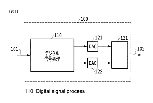
[0023] [First Embodiment]
Fig. 1 is a diagram schematically showing a
configuration of a signal generating device according to the
first embodiment of the present invention. A signal
generating device 100 includes a digital signal processing
unit 110, two DACs 121, 122, and an analog multiplexer 131.
An input signal 101 to the signal generating device 100
undergoes digital signal processing specific to the present
invention in the digital signal processing unit 110. A
digital data signal having been signal-processed, which will
be described later, by the digital signal processing unit
110 is converted into analog signals in a first DAC 121 and
a second DAC 122, respectively. Lastly, analog signal outputs
from the two DACs are converted into an output signal 102 by
the analog multiplexer 131.
[0024] It should be noted that, in the signal generating
device of the present invention, a signal inputted to the
digital signal processing unit 110 is a sampled digital
signal. The generation of an input signal to the digital
signal processing unit is typically implemented by DSP,
although not limiting to this, and an input signal to the
digital signal processing unit 110 from the DSP is digital
data information or a digital signal in which a desired
analog signal has been digitized (sampled). In addition, the
desired analog signal is generated by computing processing
within the DSP or the like, and the digitized signal is
inputted into the digital signal processing unit in the
- 18 -
CA 02996399 2018-02-22
signal generating device of the present invention. Therefore,
in the following explanation, even when there is a
description that a desired signal is to be sampled, it does
not mean that an actual analog-digital conversion is made by
an analog-digital converter (ADC). It should be noted that
it is only a concept as one process of computing processing
by the DSP, and is not an actual signal. Data directly
digitizing virtual analog waveform within the DSP is firstly
generated, and thus digitized data is supplied to the signal
generating device of the present invention to add signal
processing specific to the present invention as will be
described later. Pieces of digital data having been signal-
processed are inputted into the two DACs 121, 122, and an
actual desired analog signal is outputted through the analog
multiplexer 131. The present invention employs a combination
of the configuration of the signal generating device shown
in Fig. 1 and the signal processing specific to the present
invention which is carried out by the digital signal
processing unit so as to make the DACs 121, 122 having
insufficient output bandwidths achieve an analog output of
a broader bandwidth compared to the output bandwidth of the
DACs 121, 122 as individual units.
[0025] The two DACs
121, 122 are both connected to the
analog multiplexer 131 with wirings having the same length.
Further, as will be described later, the analog multiplexer
131 also has a symmetric configuration with respect to a
virtual signal-traveling direction from the two input portS
- 19 -
CA 02996399 2018-02-22
to an output point thereof. Accordingly, an analog signal
path from an output point of the DAC 121 to the output point
of the analog multiplexer 131 and an analog signal path from
an output point of the DAC 122 to the output point of the
analog multiplexer 131 have the same configuration. When
viewing those two signal paths along the electric signal-
traveling direction in the circuit diagram as well as in the
aspect of the actual analog circuit configuration, a
symmetric configuration is formed when regarding the
traveling direction as a virtual center axis. By using the
two DACs 121, 122 having equivalent circuit configurations
and electric properties, the two analog signal paths have
the same length, and a signal delay does not need to be
adjusted if the two DACs are driven by a clock of the same
phase.
[0026] Therefore, in
the signal generating device of the
present invention, adjustment is particularly facilitated
compared to the signal generating device using the plurality
of DACs of a conventional technique disclosed in NPL 2.
Incidentally, in the above explanation, the symmetry of a
circuit configuration in the circuit diagram or for the
analog signal path does not necessarily require the physical
shapes and locations of a device substrate of actual circuit
components and a substrate of semiconductor chips to be
identical or symmetric. If loss or delay for the signal paths
relating to the above-described two DACs is the same, the
adjustment of the DACs can still be significantly simplified.
- 20 -
CA 02996399 2018-02-22
Therefore, it should be noted that, even if the shapes and
locations of the signal paths along with analog operation of
the two DACs slightly differ, the feature of the present
invention is to be exerted as long as the signal paths from
the respective DACs to the output point of the analog
multiplexer substantially have the same length to achieve
the same loss or delay.
[0027] In the signal generating device of the present
embodiment, the analog multiplexer 131 is driven by a clock
frequency fc, and further, an output bandwidth for the DACs
121, 122 is about f0/2 and an output bandwidth for the analog
multiplexer 131 is f, or more. First of all, in explaining
the fundamental operation of the signal generating device
100 of the present invention, the operation of the analog
multiplexer 131 will be explained below.
[0028] Figs. 2A and 2B are diagrams illustrating an
operation of the analog multiplexer in the signal generating
device of the present invention. As shown in Fig. 2A, the
analog multiplexer 131 is a switching circuit that outputs
input analog signals 201, 202 of a dual system while
switching them to a high speed by using a clock signal 203
having the frequency fc. It can be assumed that this
switching circuit operates equally to an equivalent circuit
shown in Fig. 2B. In other words, it can be assumed that the
analog multiplexer 131 is a circuit to obtain, in multipliers
204a, 204b, an output 206 by multiplying input signals 201,
202 by pulse trains 203a, 203b, respectively, that
- 21 -
CA 02996399 2018-02-22
alternately cut out in a time domain and then by combining
those two multiplier outputs in an adder 205. A time waveform
for the two pulse trains 203a, 203b ideally takes a binary
of 0 and 1, which is a square wave of the frequency fc that
immediately changes values. In an actual circuit, since a
transition time of switching a switch is not zero but
requires a certain time, the time waveform is a waveform in
which its square wave is somewhat blunt.
[0029] Figs. 3A and
38 are diagrams each showing a
frequency spectrum of a pulse train to be multiplied by the
analog multiplexer. Fig. 3A schematically shows a spectrum
of the pulse train 203a multiplied by a first input signal
201 in the model of Fig. 2B, and Fig. 3B schematically shows
a spectrum of the pulse train 203b multiplied by a second
input signal 202 therein. With reference to Fig. 3A and Fig.
38, it is recognized that, when making Fourier transform on
time waveforms of the pulse trains 203a, 203b, a line
spectrum composed of a DC component and an odd multiple of
fc component can be obtained. Here, a case where the pulse
train time waveform is an ideal square wave is assumed, and
when an amplitude of the DC component (f=0) is 1, an
amplitude of a high frequency component of a frequency
(2k-1)f, for an integer k becomes 2/((2k-1)70. Incidentally,
in a case where a blunt pulse train time waveform is large
and the pulse train has a waveform that can be approximated
by a squared cosine wave, where an amplitude of the DC
component is I, an amplitude of the frequency fc component
- 22 -
CA 02996399 2018-02-22
is substantially 1/2, and the intensity for other high
frequency components is substantially zero.
[0030] Also, as a very special case, in the case of
expressing with a short pulse train whose time taking a value
of 1 for the pulse train time waveform is shorter than a
time taking a value of 0, where an amplitude of the DC
component is 1, an amplitude of the frequency fc component
becomes larger than 2/7t. As such, the analog multiplexer
expressed with the short pulse train for the pulse train
time waveform operates in a manner of, for example,
outputting the input analog signal 201 for a very short time,
and then outputting zero for a while, and subsequently
outputting the input analog signal 202 for a very short time,
and again outputting zero for a while. In other words, the
analog multiplexer expressed with the short pulse train as
such is operated in a manner close to an operation of
alternate sampling rather than switching. Such an operation
is technically possible, but not very common.
[0031] The phase of each frequency component of the pulse
train signal depends on a manner of taking a time origin for
a waveform of a pulse train. When a center point of a time
slot in which the pulse train 203a to be multiplied by the
first input signal 201 takes a value of 1 is set as a time
origin, a phase of a component of the frequency (2k-l)fc in
the spectrum shown in Fig. 3A is zero when k has an odd
number, and is n when k has an even number. Also,
irrespective of a manner of taking a time origin, a phase
- 23 -
CA 02996399 2018-02-22
difference between the components of the same frequency
between the spectrum of Fig. 3A and the spectrum of Fig. 3B
is zero in the DC component and is 7 in components other
than the DC. In the following explanation, when an intensity
of the DC component of the pulse train signal is 1, an
intensity for the frequency f, component is set to 1/r. A
value of r is a constant in the present embodiment of the
present invention.
[0032] Fig. 4 is a
diagram schematically showing an
operation of the analog multiplexer in a frequency domain in
the signal generating device of the present invention. Figs.
4(a) and 4(c) represent spectra for the first input signal
201 and the second input signal 202, and here, each of the
cases of their signal bandwidths having about f,/2 on one
side is to be considered. Fig. 4(b) represents a spectrum of
a signal after multiplying the first input signal 201 by the
pulse train 203a in the model shown in Fig. 2B, and Fig.
4(d) represents a spectrum of a signal after multiplying the
second input signal 202 by the pulse train 203b in the model
of Fig. 2B. Fig. 4(b) is a resultant of superimposing the
pulse train spectrum of Fig. 3A on the signal spectrum of
Fig. 4(a), and Fig. 4(d) is a resultant of superimposing the
pulse train spectrum of Fig. 3B on the signal spectrum of
Fig. 4(b).
[0033] As defined earlier, a signal intensity
superimposed on the frequency fc component is an intensity
of 1/r relative to a signal superimposed on the DC component.
- 24 -
CA 02996399 2018-02-22
An output signal of the analog multiplexer 131 is the
addition of signals shown in Figs. 4(b) and 4(d). Taking a
look at a phase difference between each of the frequency
components in the spectra in Figs. 4(b) and 4(d), a phase
difference between the input signals superimposed on the DC
component is zero, and a phase difference between the input
signals superimposed on the odd multiple of f, component is
n. Incidentally, since a signal component superimposed on a
frequency 3f, and the high frequency component of a higher
order does not overlap with a signal superimposed on the
frequency f, component, the signal component can easily be
removed by appropriately using a low pass filter. Further,
these high frequency components are naturally cut off in the
output side of the circuit of the analog multiplexer 131 or
a transmission path, or further, in a receiving side.
Accordingly, in the following explanation, a focus is placed
only on the signal component superimposed on the DC component
and frequency f,.
[0034] In the signal
generating device of the present
invention, in light of the operation properties of the analog
multiplexer 131 shown in Fig. 3A, Fig. 3B, and Fig. 4, signal
processing specific to the present invention is added to a
digital signal digitalizing a desired analog signal in the
digital signal processing unit 110. A focus should be placed
on an aspect that, when an upper limit frequency (output
bandwidth) of the output signal of each of the two DACs 121,
122 slightly exceeds f0/2, signal processing specific to the
- 25 -
CA 02996399 2018-02-22
present invention is added to the digital signal processing
unit 110 so that the final upper limit frequency of the
output signal 102 has a signal of a sufficiently broader
bandwidth than fc/2.
[0035] Fig. 5 is a
diagram schematically representing a
waveform synthesizing operation in the frequency domain in
the signal generating device according to the first
embodiment of the present invention. The signal processing
of the waveform synthesizing operation illustrated in Fig.
is, in the signal generating device of the present
invention in Fig. 1, is performed by elements from the
digital signal processing unit 110 to the analog multiplexer
131. All the drawings in Figs. 5(a) through 5(g)
schematically show frequencies in horizontal axis and signal
levels (amplitudes) in vertical axis. A signal below the
level of the horizontal axis shows that a phase difference
between a signal above the horizontal axis and the signal
below the horizontal axis is it. In the process of the
explanation on Fig. 5 based on the spectra of the pulse
trains shown in Fig. 3A and Fig. 3B, the phase difference
between each of the signal components is limited to the case
of 0 or it. As signal levels are simplified for an explanation
in accordance with the case of the difference between the
two phases, three-dimensional notation instead of two-
dimensional notation is required to precisely express phases
of signals. Therefore, it should be noted that each of the
diagrams of Figs. 5(a) to 5(g) is simplified for expression
- 26 -
CA 02996399 2018-02-22
in order to schematically explain signal processing in the
signal generating device of the present invention.
[0036] Fig. 5(a) is a spectrum of a desired signal to be
finally outputted from the signal generating device of the
present invention. As long as the desired signal is a real-
valued signal on a time axis and an upper limit frequency is
less than f,, any signal can be set. The desired signal is
firstly supplied to the digital signal processing unit 110
as digitized (sampled) input data, which is only virtual as
one process of the series of digital signal processing, and
digital data is directly generated by computing processing.
Input to the digital signal processing unit 110 will be
explained later again together with the block diagram of the
specific digital signal processing unit in Fig. 6 which will
be described later. In the explanation of Fig. 5 below, the
series of signal processing is schematically explained as an
operation on a frequency axis.
[0037] In the digital signal processing unit 110, first
of all, the desired signal shown in Fig. 5(a) is separated
into each of signal components shown in symbols A, B, and C
as shown in Fig. 5(b). The signal component A is a real-
valued low-frequency signal on the time axis, and signals
that combine the signal component B and the signal component
C are also real-valued high-frequency signals on the time
axis. The signal component B is a positive frequency
component, and the signal component C is a negative frequency
component. The signal component B and the signal component
- 27 -
CA 02996399 2018-02-22
C establish a mutual relation by folding into a center where
a frequency is zero and by taking a complex conjugate. At
this time, separation should be made such that a signal power
of the low-frequency signal of A substantially falls within
the range of Iff0/2 and respective signal powers for high-
frequency signals of B and C substantially fall within the
range of !ff0/2.
[0038] Next, in the digital signal processing unit 110,
among signal components separated in Fig. 5(b), the signal
component B and the signal component C are each r-folded on
the vertical axis (amplitude axis), and the signal component
C is horizontally shifted by +fõ whereas the signal component
B is horizontally shifted by -f, on the frequency axis. The
order of the r-folding operation and the horizontal shifting
operation does not matter. Each of the signal components
shifted on the frequency axis is added to the signal
component A, and a first signal having a spectrum shown in
Fig. 5(c) is obtained. The operations of r-folding the
amplitude of the spectrum and shifting them on the frequency
axis for the above-described signal component B and signal
component C are equivalent to operations of folding in the
signal component B and signal component C over a center of
fc/2 and f0/2, respectively, taking their complex conjugates,
and r-folding them to add resultants to the signal component
A.
[0039] Meanwhile, in the case where addition processing
to the signal component A, which is final processing, in the
- 28 -
CA 02996399 2018-02-22
operation of obtaining the above-described first signal is
replaced with processing of subtraction from the signal
component A, a second signal having a spectrum shown in Fig.
5(d) is obtained. Here, a value of a constant r for changing
an amplitude is, as described above, set in accordance with
the transition characteristic of switching the switch in the
analog multiplexer 131, that is, the waveform of the pulse
train in the model of Fig. 2B. In the case where the pulse
train is expressed in an ideal square wave, r=n/2 is assumed,
and in the case where the pulse train has a waveform which
is significantly blunt and which can be approximated by a
squared cosine wave, r=2 is assumed. The constant r is
normally set within the range of n/2<r<2. The power of
respective spectra in the first signal of Fig. 5(c) and the
second signal of Fig. 5(d) both substantially fall within
the frequency range of Ifl<fc/2. Therefore, both the first
signal and the second signal are sufficiently generated even
with the DAC of about f,/2 for the output bandwidth. The
first signal having the spectrum of Fig. 5(c) and the second
signal having the spectrum of Fig. 5(d) become signals as
the output analog signals from the DACs 121, 122,
respectively. Therefore, digital signals outputting the
first signal and the second signal are given to the DACs 121,
122, respectively, from the digital signal processing unit
110 in Fig. 1. In the case where the output characteristics
of the two DACs 121, 122 have frequency dependency, the
digital signal processing unit 110 can further undergo
- 29 -
CA 02996399 2018-02-22
processing for compensating this frequency dependency. The
digital signal processing unit 110 supplies digital signals
which are compensated for outputting the above-described
first signal and second signal to the DACs 121, 122.
[0040] The analog signal having the spectrum shown in
Fig. 5(c) is supplied from the DAC 121 to the analog
multiplexer 131 as a first input signal. Similarly, the
analog signal having the spectrum shown in the Fig. 5(d) is
supplied from the DAC 122 to the analog multiplexer 131 as
a second input signal. At this time, referring to the
respective spectra in Figs. 4(b) and 4(d) when multiplying
the input signals 201, 202 in the model of Fig. 2B by the
pulse trains 203a, 203b, output signals corresponding to the
first input signal and second input signal from the analog
multiplexer 131 become spectra shown in Figs. 5(e) and 5(f),
respectively.
[0041] Between signals of the respective spectra shown
in Figs. 5(e) and 5(f), the signal components of A are
mutually in the same phase for the signals superimposed on
the DC components. Meanwhile, signal components indicated as
rBs that have been obtained by r-folding the amplitude and
shifting them on the frequency axis are mutually in opposite
phases (rB and -rB), and similarly, signal components
indicated as rCs that have been obtained by r-folding the
amplitude and shifting them on the frequency axis are also
mutually in the opposite phases (rC and -rC). As to the
signals superimposed on frequency f0, signal components
- 30 -
CA 02996399 2018-02-22
indicated as A/r are mutually in the opposite phases.
Meanwhile, signals indicated as B and signals indicated as
C are mutually in the same phase, respectively. Here, the
signal indicated as B which has been superimposed on the
frequency fc in Fig. 5(e) is obtained by multiplying the
component indicated as rB that has been superimposed on the
DC component in Fig. 5(c) by the pulse train. Accordingly,
it should be noted that, as defined earlier in Fig. 3A and
Fig. 3B, the level of the frequency f component by
multiplying the pulse train is in l/r relation relative to
the DC component, and thus, the amplitude becomes (rB)x(l/r)
=B. Similarly, as to the signal indicated as C which has
been superimposed on the frequency fõ the amplitude also
becomes (rC)x(l/r) =C.
[0042] The spectra in
Figs. 5(e) and 5(f) are added by
the analog multiplexer 131, and a signal finally obtained
from the output point of the analog multiplexer 131 is a
signal having a spectrum shown in Fig. 5(g). In Fig. 5(g),
the components (rB, rC) mutually in the opposite phases
between signals shown in Figs. 5(e) and 5(f) are offset, and
only the in-phase components (A, B, and C) remain. As a
result, the desired signal shown in Figs. 5(a) and 5(b) is
obtained in the frequency range of Ifl<fc. In the frequency
ranges of f<-f0 and fc<f, an unnecessary component indicated
as B and an unnecessary component indicated as C,
respectively, remain. These unnecessary components can be
easily removed by using a low pass filter having a cutoff
- 31 -
CA 02996399 2018-02-22
frequency in the vicinity of the frequency fc. Alternatively,
as the case may be, they are naturally cut in a circuit on
the output side of the analog multiplexer 131 or a subsequent
transmission path, and further, in a circuit on the
corresponding receiving side.
[0043] With reference to the series of spectrum operation
from Figs. 5(a) to 5(g), the spectra of the signals to be
outputted from the DACs 121, 122 are 5(c) and 5(d). Therefore,
even if the output bandwidth of the DACs 121, 122 is about
fc/2, as the final output signal 102 of the signal generating
device of the present invention, any desired signal having
an upper limit frequency sufficiently larger than f,/2 (but
smaller than fc) as shown in Figs. 5(a) and 5(g) can be
obtained.
[0044] The process of operating spectra from Fig. 5(a)
to 5(g) in the present invention is expressed as follows.
The spectrum of the desired signal shown in Fig. 5(a) is
denoted as Strg(f), while the signal component A, signal
component B, and signal component C in Fig. 5(b) are denoted
as SAW, SB(f), and Sc(f), respectively. Here, spectrum Si(f)
of an output analog signal for the first DAC 121 shown in
Fig. 5(c) and spectrum S2(f) of an output analog signal for
the second DAC 122 shown in Fig. 5(d) are each expressed as
follows:
Stry(f)=SA(f) + SB(f) + Sc(f) : Sc(f)=SB* (¨f)
- 32 -
CA 02996399 2018-02-22
(f)=SA (n+riSB (i+ic)-1-Sc(f ¨ fc)}
Sz(f)=SA(f) rtSs(f-fic)+Sc(f fc)) Equations (1)
[0045] Meanwhile, in the operation model of the analog
multiplexer in Fig. 2B, when the components of the frequency
range of If1,3fc are disregarded, spectra P(f) and P2(f) for
the pulse trains multiplied by the first input signal and
the second input signal sent to the analog multiplexer,
respectively, are given by the following equations:
Pi(f)1=-216M+ 6(i fc)+6 (i+ ic))
1fc)+6(f+fc)}
P2 (f)= f 6(f) 6(f ¨ Equations (2)
[0046] Here, 6 is a Dirac delta function. When a
superimposing computation is denoted by a symbol *, the
output signal S0(f) of the analog multiplexer 131 shown in
Fig. 5(g) as a result of Equations (1) and Equations (2) is
given by the following equation:
S0(f)=P1(f) *S1(f)+P2(f) * S2(f)
1 1
fc) ¨ Sz(f ¨ fe)+Si(f+fc) ¨ 52(f +fc)11
=SA(f)+SB(f)+Sc(f)+SB(f+2f,)+Sc(f ¨ 2fc)
- 33 -
CA 02996399 2018-02-22
:"---Stry(n+SB(f+21.,)+Sc(f-2fc.) Equation (3)
[0047] As in Equation (3), the output signal S0(f) of
the analog multiplexer 131 is a signal in which the signal
component B is horizontally shifted by -2f0 on the frequency
axis and the signal component C is horizontally shifted by
+2f, on the frequency axis are added to the desired signal
Strg(f). It is understood from the above-described Equation
(3) that the processing is identical to processing performed
by the digital signal processing unit 110 explained in Figs.
5(c) and 5(d), and thus the processing explained in Fig. 5
and the processing obtained from Equation (3) are consistent
with each other. As described above, the spectrum of the
desired signal Strg(f) substantially has a signal level of
zero in the range of !ff,. Therefore, the signal power of a
signal component SD(f+2f,) in Equation (3) is substantially
zero in f-f, and the signal power of a signal component
Sc(f-2f,) therein is substantially zero in f-fõ and thus
they do not overlap with the spectrum St,g(f) of the desired
signal on the frequency axis.
[0048] Incidentally, in the explanations using the above
equations, an extrinsic scaling factor is omitted. In order
to describe the actual circuit operation of the signal
generating device of the present invention, it is necessary,
for example, to multiply a constant corresponding to a loss
or gain (when an amplifier circuit is included) of the analog
multiplexer 131 by the right side of Equation (3).
- 34 -
CA 02996399 2018-02-22
[0049] As described above, a role produced by the digital
signal processing unit 110 in the signal generating device
of the present invention is to generate digital signals and
to supply them to each of the DACs 121, 122 so that the
respective output analog signals from the two DACs 121, 122
become signals having the spectra shown in Figs. 5(c) and
5(d). In order to do so, in accordance with a desired signal,
respective signals corresponding to Figs. 5(c) and 5(d) are
generated in the digital domains, and, if the DACs 121, 122
have the output characteristics of frequency dependency,
processing to compensate this should be performed at the
same time.
[0050] Fig. 6 is a block diagram illustrating a
configuration and flow of the digital signal processing unit
according to the first embodiment of the present invention.
The digital signal processing unit 110 in Fig. 6 is
represented as a functional block diagram, but each of block
functions of the digital signal processing unit 110 can be
performed by the computing processing using DSP, for example.
Therefore, Fig. 6 can be recognized to show a substantial
flow of computation that is performed in the direction of
arrows. A part of processing in each block can be, of course,
achieved by hardware processing, or can be achieved by the
combination of hardware processing and computing processing.
Processing in each functional block in the digital signal
processing unit 110 will be explained below in order along
the flow of signals.
- 35 -
CA 02996399 2018-02-22
[0051] As the input signal 101 for the signal generating
device of the present invention, a digital signal in which
a desired signal is sampled with a sampling rate fo is used.
As described earlier, the input signal 101 is a signal in
which a desired signal to be generated is generated in the
digital domain, and thus, no actual desired signal exists.
The sampling rate f,0 is set to a value larger than twice the
upper limit frequency of the spectrum Sug(f) of the desired
signal. As is evident from a sampling theorem, this setting
allows handling of the desired signal in the digital domain
without substantially losing information. For simplification,
the analog multiplexer 131 is assumed to have ideal
characteristics in which a frequency response on the output
side is flat. It is general that a multiplexer actually has
a response characteristic of attenuation in the high-
frequency side. In such a case, as the input signal 101, a
digital signal that further undergoes processing of
compensating the response characteristic of the analog
multiplexer 131 for a signal in which a desired signal is
sampled is inputted.
[0052] In the band separation unit 611 in Fig. 6, the
inputted input signal 101 is separated into a low-frequency
signal 661 and a high-frequency signal 662. The low-frequency
signal 661 is the signal component indicated as A in Fig.
5(b), that is, this corresponds to the signal indicated as
SA(f) in Equations (1). The high-frequency signal 662 is the
signal component indicated as B in Fig. 5(b) and the signal
- 36 -
CA 02996399 2018-02-22
component indicated as C, that is, this corresponds to the
signal indicated as S(f)+S(f) in Equations (1).
Specifically, for instance, using a digital low pass filter
(LPF) having the cutoff frequency of about f,/2, a low
frequency component of the input signal 101 is cut out to
obtain the low-frequency signal 661. Furthermore, the low-
frequency signal 661 obtained from a copy of the input signal
101 is subtracted to obtain the high-frequency signal 662.
At this time, a passage gain in a passband of the LPF is
assumed as 0 dB.
[0053] As another method, using a high pass filter (HPF),
the low-frequency signal 661 can be obtained by obtaining
the high-frequency signal 662 directly from the input signal
101 and then by subtracting it from the input signal 101.
Alternatively, the LPF and the REF can be separately used to
obtain the low-frequency signals 661 and 662, respectively,
from the input signal 101. As the LPF, for example, a finite
impulse response (FIR) filter or the like having cosine roll-
off characteristics of the cutoff frequency f,/2 can be used.
As described above, various implementation methods can be
employed for digital signal processing in the signal
generating device of the present invention, and specific
signal processing methods are not limited only to those
described in the specification including processing for
other blocks which will be described later.
[0054] In the folding unit 621 in Fig. 6, a positive
frequency component of the high-frequency signal 662 in the
- 37 -
CA 02996399 2018-02-22
frequency domain is shifted by -fc, and a negative frequency
component thereof is shifted by +fc, and further, the
amplitude is r-folded to output a folded signal 663.
Specifically, using Hilbert transform, for example, the
following computation should be performed. The Hilbert
transform can be generally achieved by using a FIR filter.
In other words, assuming that Hilbert transform of x(n) is
Hilbert[x(n)], the following equation is given:
x(n) j = Hilbert[x(n)]
x+(n), _____ 2 Equation (4)
where x(n) (n is an integer index) is the high-
frequency signal 662 to be inputted, x+(n) is a positive
frequency component, and x_(n) is a negative frequency
component.
[0055] Furthermore, an operation of shifting the
spectrum by fc in the frequency domain corresponds to
multiplying it by exp( j27cfcri/f5d in the time domain.
Therefore, in the folding unit 621, the computation of the
following equation is performed to output a folded signal
663y(n):
fc lc
y(n)=r = [x+(n) = exp (¨j2ir n)+x_(n) = exp n))
I sO sO
=r = [x(n) = cos (271--, +H ilbert[x(n)] = sin (21r n)} Equation
(5)
Iso
[0056] The folded signal 663 obtained by Equation (5)
- 38 -
CA 02996399 2018-02-22
corresponds to. the signal component indicated as rB in the
frequency domain shown in Fig. 5(c) and the signal component
indicated as rC therein. In other words, this corresponds,
in Equations (1), to signals in which each of second clauses
rtSB(f+f,)+Sc(f-fc)) of the spectra Sl(f), S2(f) of the analog
signals to be outputted from the two DACs 121, 122 sampled
with the sampling rate fso in the time domain. In practice,
the computation in the 2nd line of Equation (4) and Equation
(5) needs to be performed by delaying the first clause x(n)
by a delay caused by Hilbert transform, but for
simplification, delay operation is omitted in the
description.
[0057] In resampling
units 631, 632 in Fig. 6, the
sampling rates for the digital signals of the low-frequency
signal 661 and folded signal 663 are converted from f,D to
fsl, respectively. Here, fs1 is a sampling rate for the DACs
121, 122, and, as described above, it is necessary to set a
value larger than twice the upper limit frequency of the
output signal of Si(f) for the DAC 121 and the output signal
of S2(f) for the DAc 122. The upper limit frequency for Si(f)
and S2(f) is somewhat larger than about fc/2 and smaller than
the upper limit frequency of the desired signal Strg(f), and
therefore can be assumed to be f51<f,0 in general. However,
fs1=f0 is also possible, and in such a case, the resampling
units 631, 632 can naturally be omitted. Assuming f31=f50
refers to a case where, for example, a sampling rate operable
for the DACs 121, 122 is relatively larger by about four
- 39 -
CA 02996399 2018-02-22
times the output bandwidth f0/2 of that DAC.
[0058] In an addition unit 641 in Fig. 6, the resampled
folded signal 663 is added to the resampled low-frequency
signal 661, a first signal 671 is generated. The first signal
671 corresponds to the sum of all spectra shown in Fig. 5(c),
that is, corresponds to the first signal denoted as Si(f) in
Equations (1). In the subtraction unit 642, a second signal
672 is generated by subtracting the resampled folded signal
663 from the resampled low-frequency signal 661. The second
signal 672 corresponds to the sum of all spectra shown in
Fig. 5(d), that is, corresponds to the second signal denoted
as S2(f) in Equations (1). It should be noted that the first
signal 671 and the second signal 672 are still digital
signals.
[0059] Therefore, the present invention may be carried
out using a signal generating device comprising: a digital
signal processing unit 110; two digital-to-analog converters
(DACs) 121, 122; and an analog multiplexer 131 that
alternatingly switches analog signals outputted from the two
DACs with a frequency fc for outputting as analog signals,
wherein the digital signal processing unit includes: when a
signal, among desired output signals having an upper limit
frequency of less than f, made of a component having an
absolute value of a frequency being substantially fc/2 or
less is assumed as a low-frequency signal (signal component
A), and when, for a positive frequency component (signal
component B) and a negative frequency component (signal
- 40 -
CA 02996399 2018-02-22
component C) which are made of a component having an absolute
value of a frequency being substantially fc/2 or more among
the desired output signals, a signal in which the positive
frequency component is shifted by -f, on a frequency axis
and a signal in which the negative frequency component is
shifted by +f, on the frequency axis are assumed as a folded
signal, means for generating a first signal 671 that is equal
to a signal obtained by multiplying the folded signal by a
constant (r) and adding a resultant to the low-frequency
signal; and means for generating a second signal 672 that is
equal to a signal obtained by multiplying the folded signal
by the constant (r) and subtracting a resultant from the
low-frequency signal, and wherein: a digital signal
corresponding to the first signal generated in the digital
signal processing unit is inputted into one of the two DACs;
and a digital signal corresponding to the second signal
generated in the digital signal processing unit is inputted
into the other one of the two DACs.
[0060] Lastly, in
compensation units 651, 652 in Fig.6,
frequency response characteristics intrinsically owned by
the DACs 121, 122 are compensated. Specifically, a filter
having a response characteristic of a reverse characteristic
that approximately cancels the frequency response
characteristics of the DACs 121, 122 may be employed. Such
compensation processing is sometimes called as pre-
equalization and is commonly performed in a high-speed
communication system using the DAC. Output digital signals
- 41 -
CA 02996399 2018-02-22
from the compensation units 651, 652 are supplied to the
DACs 121, 122, respectively, as outputs of the digital signal
processing unit 110. As for the output of the DAC 121, the
first signal having the spectrum shown in Fig. 5(c) as the
analog signal and which is denoted as Si(f) in Equations (1),
is obtained. Similarly, as for the output of the DAC 122,
the second signal having the spectrum shown in Fig. 5(d) as
the analog signal and which is denoted as S2(f) in Equations
(1) is obtained. In the case where the frequency response
characteristics of the DACs 121, 122 are substantially flat
within the bandwidths up to the upper limit frequency of the
first signal Si(f) and second signal S2(f), the compensation
units 651, 652 can be omitted.
[0061] In the case
where the sampling rate f,0 of the
input signal 101 in the signal generating device of the
present invention satisfies a certain condition, the
computation in the folding unit 621 in Fig. 6 can be
performed without using the above-described Hilbert
transform. Another implementation method of performing
computation in the folding unit 621 without using the Hilbert
transform will be shown below. Here, the high-frequency
signal 662 to be inputted is denoted as x(n), and the
spectrum of x(n) (discrete-time Fourier transform) is
denoted as X(f). The spectrum X(f) is a periodic function of
periodic f30 on the frequency axis, and can be represented
as the following equation using SB(f) and Sc(f) in Equations
(1):
- 42 -
CA 02996399 2018-02-22
+co
X(f)= {SB(f ¨ kfs0)+Sc(f ¨ k[30)} Equation (6)
[0062] A signal obtained by multiplying x(n) by the
cosine wave of the frequency fc in the time domain and by
2r-folding the resultant is denoted as y' (n) as in the
following equation:
y'(n)=2r = x(n) = cos (27r-f-L. Equation (7)
Iso
[0063] At this time, Y' (f), the spectrum of
y' (n) (discrete-time Fourier transform) is represented by the
following equation:
r (f)=.2r = X(f) *45(1. ¨
2
=r ' fc)-1-X(i+ic))
=r tSB(f ¨ fc. ¨ kf50)+Sc(f ¨ fc. ¨ klso)+SB(f+fc
¨ k fso) Equation (8)+Expression (8).5c(f +I; ¨ MO) Equation (8)
[0064] Meanwhile, as described above, a signal y(n) to
be obtained as the output of the folding unit 621 is a signal
in which r(Sp(f+f,)+Ec(f-fc)) in Equations (1) is sampled with
the sampling rate f,0 in the time domain. Therefore, Y(f),
the spectrum of y(n) (discrete-time Fourier transform) is
represented by the following equation:
- 43 -
CA 02996399 2018-02-22
+00
Y(f)=r {SB(f+ f, ¨ k fso)+Sc(f ¨ f, ¨ k fs0)) Equation (9)
k¨co
[0065] With reference to Equation (9) and Equation (8),
it is recognized that, when filtering processing so as to
remove SB(f-fõ-kfso) in the first clause of the third row on
the right side and Sc(f+fc-kfad in the fourth clause thereof
in Equation (8) is performed for y' (n) which corresponds to
Equation (8), y(n) can be obtained.
[0066] Fig. 7A and Fig. 7B are spectrum diagrams
illustrating the computing operation of the folding unit
when Hilbert transform is not used. Hereafter, S2(f-fõ-kfa0)
in the first clause of the third row on the right side in
Equation (8) will be focused. The first clause of Equation
(8) represents a spectrum which is obtained by r-folding the
signal component B in Fig. 5(b) and shifting it by +f, on
the frequency axis and which repeatedly appears in an f50
interval. Here, the upper limit frequency of the signal
component B is denoted as fmax and the lower limit frequency
is denoted as fmin. As for a spectrum of the first clause of
Equation (8), in the case where the sampling rate fso of the
input signal 101 is s0 ¨fMa f > +f
¨x ¨Of as shown in Fig. 7A, a
component of k=0, that is, S9(f-fõ), only appears in a Nyquist
band, that is, Ifl<fs0/2. This can be easily removed by using,
for example, the LPF of the cutoff frequency of about f,.
[0067] Meanwhile, in the case where the sampling rate fso
of the input signal 101 is fs0 ¨M <f
¨ax ¨+f
cr as shown in Fig. 7B,
the component of k=-1, that is, SB(f-fo+fad appears on the
- 44 -
CA 02996399 2018-02-22
=
negative frequency side. The upper limit frequency of the
unnecessary component that appears on this negative
frequency side is fmax+fc-fsof whereas the lower limit
frequency of SE(f+fc), which is a necessary component, is
fm1-f0. Therefore, if the relation of fmax+fc-fso<fm,,,-f, is
established, this unnecessary component which appears on the
negative frequency side can be removed by using the LPF of
the cutoff frequency of substantial Ifmln-fd. The above
discussion is similarly established for Sc(f+f0-kfõ.0) in the
fourth clause of the third row on the right side in Equation
(8) as well. In other words, if fmax+fc-fs,o<fmin-fc, as for
processing in the folding unit 621, an unnecessary frequency
component may be removed by an appropriate LPF after
multiplying the input signal represented in Equation (7) by
the cosine wave of the frequency fc.
[0068] Furthermore, when f,0=2fc, the unnecessary
component SB(f-fc+fso) resulted from multiplication of the
cosine wave matches exactly with the necessary component
SB(f+f,), and therefore, there is no need to make removal.
Accordingly, processing in the folding unit 621 is more
simple, and a desired folded signal of y(n) can be obtained
only by the computation in the following equation without
using the LPF.
fc.
y(n)=r = x(n) = cos t 27r n =r = x(n) = cos(n-n) Equation (10)
[0069]
In other words, the signs of r.x(n) alternately
- 45 -
CA 02996399 2018-02-22
inverted may be assumed as y(n). In order to confirm this,
the spectrum of Equation (10) (discrete-time Fourier
transform) Y(f) is sought for and the following equation can
be expanded:
r
Y(f)=-2 {Ss(f ¨f,¨kfc0)+sc(f ¨ f,¨ kf,0)+sB(f+f,¨ kf,0)+sc(f+f,¨kf,0)1
ic¨co
[Stiff ¨ (1+20 fc}+Sjf
2
¨ (1+2k)fc)+SB{f-41 2k)fj+Sc[f+(1 ¨ 2k)f,)]
B c
(f+f ¨ fc)+Sc(f ¨ fc ¨ 2/cfc)) Equation (11)
k ¨co
[0070] Equation (11) is identical to the result indicated
as fs0=2f, in Equation (9).
[0071] Furthermore, as another implementation method,
the entire processing flow in the digital signal processing
unit 110 shown in Fig. 6 can be achieved by using processing
in the frequency domain instead of using the time domain as
explained above. For instance, a time-domain signal of the
input signal 101 is firstly converted into a frequency-domain
signal at the pre-stage of the band separation unit using
the discrete Fourier transform (DFT). Thereafter, processing
of each of the band separation unit 611, folding unit 621,
addition unit 641, subtraction unit 642, and compensation
units 651, 652 are all performed in the frequency domain.
Lastly, the outputs of the frequency-domain signals of the
- 46 -
CA 02996399 2018-02-22
compensation units 651, 652 are reconverted into the time-
domain signals using inverse-discrete Fourier transform
(IDFT), which are outputted to the DACs 121, 122. In the
frequency domain, each of the operations for band separation
and the compensation of DAC response characteristics can be
easily achieved by multiplying them by an appropriate filter
shape function. Also, the folding operation (frequency
shift) can be easily achieved by index replacements
(rearrangement of data points) in the frequency domain. In
this case, block processing for every number of points for
DFT and IDFT is to be performed, and overlapping processing
which is typically used may be performed to remove the
influence of the inter-block interference.
[0072] As described
above, variations of different
implementation methods for processing in each of the blocks
in the digital signal processing unit 110 have been presented,
but the feature of the present invention does not depend on
the method of implementing specific computing processing.
The present invention has a feature of operating the digital
signal processing unit 110 so as to output, to the analog
multiplexer 131, the first signal having the spectrum shown
in Fig. 5(c) and the second signal having the spectrum shown
in Fig. 5(d) as the analog signals outputted from the two
DACs 121, 122. In other words, the following advantageous
result specific to the present invention is exerted such
that the digital signal processing unit 110 supplies digital
signals to the two DACs by outputting signals indicated as
- 47 -
CA 02996399 2018-02-22
=
the first signal Si(f) and the second signal S2(f) in
Equations (1).
[0073]
In other words, due to signal processing specific
to the present invention in the digital signal processing
unit 110, in the signal generating device that includes the
two DACs and the analog multiplexer, it is possible to output
any signal of a broader bandwidth compared to the output
bandwidth of individual DACs. Specifically, by combining an
on-going CMOS-DAC with the present invention, the output
bandwidth of about 30 GHz can be achieved. The band of the
single CMOS-DAC has become wider recently, and further, by
using a compound semiconductor device such as SiGe and InP,
the output bandwidth of up to about 50 GHz can be expected
by combining the device with the present invention.
[0074] Further, as is evident from the entire
configuration of the signal generating device shown in Fig.
1, each of the output points of the DACs 121, 122 through
the output of the analog multiplexer 131 forms, when two
signal paths are viewed along the traveling direction of
electric signals, a symmetric configuration by regarding the
traveling direction as a virtual central axis. Therefore,
the adjustment of the amplitude and delay of the DACs can be
suppressed to the minimum. There may be a case where the
signal generating device of the present invention needs
adjustment between the DACs caused by variations in
manufacturing semiconductor chips, adjustment between
connection cables in the device, and adjustment for
- 48 -
CA 02996399 2018-02-22
compensating the characteristic difference between the input
ports of the analog multiplexer. For instance, when one of
the DACs has a smaller output amplitude than that of the
other DAC, the other DAC needs to be adjusted so as to
suppress the output. Generally, such adjustments may only
require simple and fine tunings as long as DACs manufactured
in the same design and the same process are used. Such
advantageous results specific to the present invention do
not depend on the details of the specific implementation
method of the processing flow in the digital signal
processing unit 110 for obtaining the first signal S1(f) and
second signal S2(f)=
[0075] [Second Embodiment]
Fig. 8 is a diagram schematically showing a
configuration example of an optical transmitter including
the signal generating device according to the second
embodiment of the present invention. In the present
embodiment, a signal generating device 800 equivalent to the
signal generating device shown in Fig. 1 is incorporated
into an optical transmitter 890. The signal generating device
800 of the present embodiment is different from the signal
generating device 100 shown in Fig. 1 in an aspect that a
low pass filter (LPF) 861 is connected to an analog
multiplexer 831 at its post-stage. The LPF 861 can be
achieved by an analog LPF of the cutoff frequency of about
f,. The LPF 861 removes the signal component B which exists
in f<-f, and the signal component C which exists in f>f,,
- 49 -
CA 02996399 2018-02-22
s'
among the outputted signal spectrum shown in Fig. 5(g), as
unnecessary signal components. As described above, there may
be a case where these unnecessary components are naturally
removed due to the output characteristics owned by the analog
multiplexer 831, or, these unnecessary components can also
be removed in the receiving side of the device which is
responsive to the optical transmitter 890. As in the present
embodiment, by inserting the LPF 861 to the post-stage of
the analog multiplexer 831, these unnecessary components can
certainly be removed in the transmitting side of the device.
Due to the configuration including the LPF in the present
embodiment, an interference to a desired signal component
caused by the unnecessary component, when the nonlinearity
of a transmission path is large, for example, can be
prevented. Also, in the case where a signal generated by the
signal generating device of the present invention is
transmitted by multiplexing the frequency (wavelength) with
other signals on a carrier such as light, crosstalk to an
adjacent channel caused by the unnecessary component can be
suppressed.
[0076]
The optical transmitter 890 of the present
embodiment is an optical transmitter that uses light
intensity modulation, and is used in an optical transmission
system using an intensity modulation-direct detection system
and the like. In the present embodiment, a digital signal
processing unit 810 of the signal generating device 800
generates a baseband signal for the transmitter that uses
- 50 -
CA 02996399 2018-02-22
light intensity modulation. The signal generating device 800
outputs a real-valued digital waveform 802 in which digital
modulation and other processing which will be described later
are added to transmission information data. In the optical
transmitter 890, first of all, a symbol mapping according to
a predetermined modulation system is made in the digital
modulation unit 882 for transmission information data 881
that has underwent error correcting coding beforehand. In a
waveform shaping and compensating unit 883, pulse shaping,
channel response compensation processing (pre-equalization),
processing of compensating nonlinearity of voltage response
for an electro-optic conversion (E/0) device which is
arranged at the post-stage of the optical transmitter 890,
and the like are made. As for the signal generating device
800, digitized data that underwent the above series of
processing is supplied, as input data 801, to the digital
signal processing unit 810. Functions such as the above-
described error correcting coding, symbol mapping, pulse
shaping, and channel pre-equalization can normally be all
implemented physically by the transmitting side of the DSP.
Therefore, the input data 801 to the signal generating device
800 is typically supplied from the transmitting side of the
DSP. In the optical transmitter 890 of the present embodiment,
functions of the digital signal processing unit 810 included
in the signal generating device 800 may also be configured
to be integrally incorporated into the above-described
transmitting side of the DSP.
- 51 -
CA 02996399 2018-02-22
[0077] An analog
output signal 802 from the signal
generating device 800 is, after amplified by an amplifier
884, converted into an optical signal by an E/O device 885
and outputted to a transmission path. As the E/O device 885,
a device such as a direct modulation laser and an absorption-
type modulator integrated laser which converts an electric
signal into light intensity information is used. In the
optical transmitter 890 including the signal generating
device 800 in the present embodiment, the digital signal
processing unit 810 is operated such that two DACs 821, 822
output, to the analog multiplexer 831, the first signal
having the spectrum shown in Fig. 5(c) and the second signal
having the spectrum shown in Fig. 5(d) as output analog
signals. In the present embodiment, the digital signal
processing unit 810 generates the baseband signal for the
transmitter that uses light intensity modulation. An
advantageous result of the present invention is exerted when
the digital signal processing unit 810 supplies digital
signals by outputting signals indicated as the first signal
Si(f) and the second signal S2(f) in Equations (1) to the two
DACs. Due to the signal processing specific to the present
invention in the digital signal processing unit 810, the
signal generating device including the two DACs 821, 822 and
the analog multiplexer 831 allows outputting any signal of
a broader bandwidth compared to the output bandwidth for
individual DACs. Further, as is evident from the entire
configuration of the digital signal processing unit 810 shown
- 52 -
CA 02996399 2018-02-22
in Fig. 8, each of the output points of the DACs 821, 822
through the output of the analog multiplexer 131 forms, when
two signal paths are viewed along the traveling direction of
electric signals, a symmetric configuration by regarding the
traveling direction as a virtual central axis. Therefore, as
in the signal generating device of the first embodiment, the
adjustment of the amplitude and delay of the DACs can be
suppressed to the minimum in the present embodiment as well.
[0078] [Third Embodiment]
Fig. 9 is a diagram schematically showing a
configuration of an optical transmitter including the signal
generating device according to the third embodiment of the
present invention. An optical transmitter 990 includes four
signal generating devices 900a to 900d. A configuration of
each of the signal generating devices 900a to 900d is
identical to the signal generating device 800 of the second
embodiment shown in Fig. 8. The optical transmitter 990 of
the present embodiment is a transmitter using the intensity
and phase of two light-orthogonal polarization waves, and is
used in a coherent optical transmission system and the like.
When the two orthogonal polarization waves are represented
as an X polarization wave and a Y polarization wave, an in-
phase component as I, and an orthogonal phase component as
Q, each of the signal generating devices 900a to 900d
generates four types of real-valued waveforms which
correspond to an I component of X polarization wave, a Q
component of X polarization wave, an I component of Y
- 53 -
CA 02996399 2018-02-22
polarization wave, and a Q component of Y polarization wave.
[0079] In the optical
transmitter 990, first of all, a
symbol mapping according to a modulation system using the
two orthogonal polarization waves is made for transmission
information data 981 that has underwent error correcting
coding beforehand. Further, after undergoing pulse waveform
shaping and necessary channel pre-equalization, digitized
data corresponding to each of the real-valued waveforms for
the I component of X polarization wave, the Q component of
X polarization wave, the I component of Y polarization wave,
and the Q component of Y polarization wave is supplied to
each of the signal generating devices 900a to 900d as pieces
of input data 901a to 901d. The analog output signals from
the signal generating devices 900a to 900d are amplified by
amplifiers 984a to 984d, respectively. The amplified signals
are inputted to a polarization multiplexed IQ modulator 986
to which a transmission laser 985 is connected and outputted
to a transmission path as an optical signal. In the optical
transmitter 990 of the present embodiment as well, functions
such as the error correcting coding, symbol mapping, pulse
shaping, channel response compensation, response
nonlinearity compensation for the IQ modulator can all be
implemented at the transmitting side of the DSP. Therefore,
input data 901a to 901d to the signal generating devices
900a to 900d can be typically supplied from the transmitting
side of the DSP. In the optical transmitter 990 of the
present embodiment, each of the functions of digital signal
- 54 -
CA 02996399 2018-02-22
processing units 910a to 910d included in the signal
generating devices 900a to 900d may also be configured to be
integrally incorporated into the above-
described
transmitting side of the DSP.
[0080] In the optical
transmitter 990 including the
signal generating devices 900a to 900d in the present
embodiment as well, in each of the signal generating devices,
that is, for example, in the signal generating device 900a,
the digital signal processing unit 910a is operated such
that two DACs 921a, 922a output the first signal having the
spectrum shown in Fig. 5(c) and the second signal having the
spectrum shown in Fig. 5(d) to an analog multiplexer 931a as
output analog signals. In the signal generating devices 900a
to 900d of the optical transmitter 990 in the present
embodiment, each of the digital signal processing units
generates four types of baseband signals for a modulator
that uses modulation using two orthogonal polarization waves.
An advantageous result of the present invention is exerted
when each of the digital signal processing units supplies
digital signals by outputting signals indicated as the first
signal S(f) and the second signal S2(f) in Equations (1) to
the two corresponding DACs. Due to the signal processing
specific to the present invention in the digital signal
processing unit, the signal generating device including the
two DACs and the analog multiplexer allows outputting the
baseband signal of a broader bandwidth compared to the output
bandwidth for individual DACs. As in each of the first
- 55 -
CA 02996399 2018-02-22
embodiment and each of the second embodiment, the adjustment
of the amplitude and delay of the DACs can also be suppressed
to the minimum.
[0081] [Fourth Embodiment]
Fig. 11 is a diagram showing a configuration of the
digital signal processing unit in the signal geherating
device according to the fourth embodiment of the present
invention. The entire configuration of the signal generating
device of the present embodiment is identical to the signal
generating device 100 of the first embodiment shown in Fig.
1, but is different from the first embodiment in the aspect
of providing, as a digital signal processing unit, a digital
signal processing unit 1110 that performs processing shown
in Fig. 11. In addition, the signal generating devices
according to the first embodiment through the third
embodiment can generate any desired signal less than the
upper limit frequency fõ, when the clock frequency of the
analog multiplexer is f,. A signal that can be generated by
the signal generating device of the present embodiment is
limited to a multicarrier signal such as an orthogonal
frequency-division multiplexing (OFDM) signal and a discrete
multi-tone (DMT), and thus the signal generating device of
the present embodiment is adapted to the multicarrier signal.
[0082] A general flow of generating a multicarrier signal
such as the OFDM signal and the DMT is, for example, shown
in NPL 3 as follows. Its outline is, first of all, to convert
input data from serial to parallel (S/P conversion) in a
- 56 -
CA 02996399 2018-02-22
digital domain to split it into subchannels, and to map data
of each of the subchannels to a transmission constellation
to create a complex symbol value (subsymbol value) for each
frequency subcarrier. Next, by inverse-discrete Fourier
transforming (IDFT) a subsymbol sequence, a time domain data
sequence corresponding to a signal in which each subcarrier
is modulated with the corresponding subsymbol is obtained.
Lastly, it is parallel-serial converted (P/S conversion) and
sent to the DAC to obtain a multicarrier signal as a DAC
output. These series of processing are performed as block
processing for every number of points in the IDFT. In most
cases, at the pre-stage or post-stage of the P/S conversion,
a guard interval such as a cyclic prefix (CP) is added to
each symbol so that an inter-block interference caused by
dispersion of transmission paths or the like can be removed
on the receiving side. Also, an inverse fast Fourier
transform (IFFT), which is an algorithm to rapidly perform
the IDFT, is generally used for conversion from a frequency-
domain signal to a time-domain signal. In the case of the
OFDM, the same modulation constellation for all subcarriers
is basically used, and in the case of the DMT, a modulation
constellation in which modulation multilevels and intensity
are optimized for every subcarrier according to the frequency
response characteristic of the transmission path is used
(NPL 4).
[0083] In the case
where the output of a multicarrier
signal of a broader bandwidth compared to an output bandwidth
- 57 -
CA 02996399 2018-02-22
for individual DACs needs to be obtained using the principle
of the signal generating device of the present invention as
explained in Figs. 5(a) to 5(g), the multicarrier signal may
simply be set as a desired signal in the first embodiment.
In other words, a digital signal processing circuit that
performs multicarrier signal generation processing shown in
NPL 3 is separately provided outside the signal generating
device of the present invention, and an outputted digital
data signal from the digital signal processing circuit may
be applied to the input signal 101 to be sent to the digital
signal processing unit 110 in Fig. 6. However, in the case
where a desired signal is a multicarrier signal, the
multicarrier signal can be more efficiently generated by
including the processing of multicarrier signal generation
processes in the digital signal processing unit of the
present invention, instead of separately providing the
digital signal processing circuit for generating the
multicarrier signal as shown in NPL 3. A configuration
example of further introducing processing of modified
multicarrier signal generation processes into the digital
signal processing unit of the signal generating device of
the present invention, its operation, and its implementation
method will be explained below.
[0084] Fig. 10 is a
diagram illustrating processing until
an OFDM signal is generated in the frequency domain by the
signal generating device of the present embodiment. Fig.
10(a) shows a baseband OFDM signal, which is a desired signal.
- 58 -
CA 02996399 2018-02-22
Here, the number of subcarriers is denoted as M, a subsymbol
value for m-th (m=0, 1, ..., M-1) subchannel as cm(t), and a
subcarrier frequency as mAf. Therefore, Af is a subcarrier
frequency interval. Further, Af and f, are set so that the
relation of the following equation is established between
the drive clock frequency f, of the analog multiplexer 131
in the signal generating device and a p-th subcarrier
frequency pAf:
PZif=-2 Equation (12)
[0085] Similar to the signal generating device of the
first embodiment, the entire upper limit frequency of a
desired signal is assumed to be less than the clock frequency
fc of the analog multiplexer. Accordingly, the relation of
M-1<2p is established in Equation (12). Each complex symbol
value cm(t) varies depending on a symbol rate Af, but a time
variation t is omitted in each of the diagrams illustrated
in Fig. 10 for simplification.
[0086] A desired OFDM signal having a spectrum shown in
Fig. 10(a) is divided into different frequency components to
perform the following signal processing based on a concept
similar to the series of digital signal processing in the
frequency domain shown in Figs. 5(a) to 5(g). Similar to
Figs. 5(a) to 5(d), the desired signal is separated into a
low-frequency signal indicated as A, a high-frequency signal
- 59 -
CA 02996399 2018-02-22
(positive frequency component) indicated as B, and a high-
frequency signal (negative frequency component) indicated as
C. Further, the series of operation are performed such that
the respective amplitudes of the signal component B and the
signal component C are r-folded in a vertical axis direction,
and the signal component C is horizontally shifted by +f,
and the signal component B is horizontally shifted by -f, in
their lateral directions, respectively, to superimpose them
on the signal component A. Provided, however, in the present
embodiment, instead of cutting out each signal component by
using the LPF or the like from the desired signal generated
in the digital domain, the above-described amplitude change
and frequency shift operation are made on the frequency
domain in the stage of signal generation. In other words, as
shown in Fig. 10(a), 0 to p-th subchannel signals are treated
as a signal component A, the positive frequency component of
p+1 to M-lth subchannel signals as a signal component B, and
the negative frequency component as a signal component C,
and further, the signal component B and the signal component
C are shifted and are superimposed on the signal component
A in the frequency domain at the generation stage of the
OFDM signal. Operation at the time of generating the OFDM
signal will be explained below in detail.
[0087] Fig. 10(b)
shows a first spectrum after folding
the signal component B and the signal component C, which are
the high-frequency signals of the OFDM signal, and this state
corresponds to the state of the spectrum shown in Fig. 5(c).
- 60 -
CA 02996399 2018-02-22
In order to generate the spectrum of Fig. 10(b), an IDFT
computation may be performed by r-folding the p+lth through
M-lth subsymbol values of OFDM signal for a desired signal
at the OFDM signal generation stage beforehand, taking their
complex conjugates, and adding them to p-lth through 2p-
M+1th subsymbol values. Fig. 10(c) shows a second spectrum
after folding the signal component B and the signal component
C, which are the high-frequency signal of the OFDM signal,
and this state corresponds to the state of the spectrum shown
in Fig. 5(d). In order to generate the spectrum of Fig. 10(c),
the addition in the above-described signal generation
procedure shown in Fig. 10(b) may be replaced with
subtraction. The setting of a coefficient r value for
changing amplitudes is identical to that of the first
embodiment. The upper limit frequency of a signal having the
spectrum shown in Figs. 10(b) and 10(c) is substantially
f0/2+Af/2. If the subcarrier frequency interval Af is
sufficiently small, the waveform can be sufficiently
generated even with the DACs having the output bandwidth of
about f,/2.
[0088] When a signal having the first spectrum of Fig.
10(b) and a signal having the second spectrum of Fig. 10(c)
are outputted from the DACs 121, 122, respectively, due to
the same principle as the spectrum operation shown in Figs.
5(e) to 5(g), a spectrum signal shown in Fig. 10(d) as the
output of the analog multiplexer 131 can be obtained. As in
the spectrum shown in Fig. 5(g), each of unnecessary signal
- 61 -
CA 02996399 2018-02-22
component B and signal component C remains in the frequency
domain of f<-f, and f(<f. These unnecessary signal components
can be easily removed by using the low pass filter having a
cutoff frequency in the vicinity of frequency fc. As the case
may be, they are naturally cut on the output side of a
circuit of the analog multiplexer or the transmission path,
and further, on the receiving side of the device which is
responsive to the signal generating device of the present
invention. As such, even if the output bandwidth for the
DACs 121, 122 is about f,/2, in the signal generating device
of the present embodiment, as a final output signal of the
analog multiplexer 131, any OFDM signal having the upper
limit frequency sufficiently larger than fc/2 (but smaller
than fõ) can be obtained. The example of the series of
processing of generating the OFDM signal explained in Fig.
can also be applied to a multicarrier signal such as a
DMT signal.
[0089] The series of processing on the frequency domain
for the above-described multicarrier signal along with Fig.
10 can be expressed in the following equation. First of all,
time waveform strg(t) and spectrum strq(f) of a desired signal
can be expressed in the following equation when omitting an
extrinsic scaling factor.
m-1
strg (t)= [cm (t) = exp (j2n-mAft) +cni* (t) = exp(¨j2TrmAft)}
771-0
- 62 -
CA 02996399 2018-02-22
M-1
Strg (f)= tc.(f ¨ mAf)+c* (f+mAn} Equation (13)
m=0
[0090] Provided, however, Cm(f) indicates Fourier
transform of cm(t). The pulse waveform of cm(t) is ideally a
rectangular pulse having a time width 1/Af, and in this case,
the envelope curve of Cm(f) is a sinc function having a null
point on the integral multiple of Af on the frequency axis.
Spectrum SA(f) for the signal component A which is the low-
frequency signal, spectrum SH(f) for the signal component B
and spectrum Sc(f) for the signal component C, which are the
high-frequency signals, in Fig. 10(a) are each expressed in
the following equations:
SA(f)=I{Cm(f ¨ mAf.)+Cm* (f+mAf)}
in=o
m-i
SB(f)= Cm(f ¨ mg)
m=p+1
M-1
Sc (f)= C,*õ(f+mAf)
m=p+1
Strg (f)=SA(f)+SB(f)+Sc(f) Equations (14)
[0091] Further, spectrum S1(f) for the output analog
signal of the DAf 121 shown in Fig. 10(b) and spectrum S2(f)
- 63 -
CA 02996399 2018-02-22
for the output analog signal of the DAC 122 shown in Fig.
10(c) are as follows:
m-i
Si(f)=SA(f)+r [C1õtf+(2p ¨ m)Af}+C,tf ¨ (2p ¨ m)Af}]
m=p+1
=SA (f)+TISB(f+f,)+Sc(f ¨ fc)}
m-1
S2 (f)=SA (r) ¨ r [C7ntf+(2p ¨m)4f)+Cm* ¨ (2p
¨ m)An]
m=p+1
=SA(f) ¨ rtSB(f+fc)+Sc(f ¨ lc)} Equations (15)
[0092] With reference to Equations (15), it can be
understood that the relation identical to Equations (1)
explained in the first embodiment is eventually established
between spectra for SA(f), SB(f), Sc(f), Si(f) and S2(f).
Therefore, spectrum S0(f) for the output signal of the
analog multiplexer 131 has a shape identical to that of
Equation (3), and in the signal generating device of the
present embodiment, signal processing identical to the first
embodiment is performed and the same advantageous result can
be obtained. In other words, in the signal generating device
of the present embodiment, the output of a multicarrier
signal of a broader bandwidth compared to an output bandwidth
for the individual DACs 121, 122 can be achieved.
[0093] With reference to Fig. 11 again, the signal
processing flow of the digital signal processing unit 1110
- 64 -
CA 02996399 2018-02-22
in the signal generating device of the present embodiment
will be explained. The digital signal processing unit 1110
of Fig. 11 is represented as a functional block diagram, but
each of the functions in the digital signal processing unit
1110 can be performed by computing processing using the DSP,
for example, and therefore, can be viewed as substantially
indicating a computing operation flow to be performed in
arrow directions. It is possible, of course, to implement at
least a part of processing for each block by hardware
processing or to implement combination of hardware
processing and computing processing. Processing for each of
the functions in the digital signal processing unit 1110
will be explained below in order along the flow of signals.
[0094] Signal processing for the digital signal
processing unit 1110 is basically block processing for every
symbol time. Here, for simplification, only the processing
for a certain symbol time will be focused on, where a
subsymbol value for the symbol time is simply denoted as cm.
Input data 1101, which is information data to be transmitted
by the OFDM signal, is divided into subchannels by an S/P
conversion unit 1111, and further, they are converted into
subsymbol values co to cm_i for each of the frequency
subcarriers by a symbol mapping unit 1121. A procedure up to
subsymbol value generation is identical to the normal
procedure of generating the OFDM signal shown in NPL 3 and
the like.
[0095] Next, in a
complex conjugate conversion unit 1131,
- 65 -
CA 02996399 2018-02-22
subsymbol values cp+1 to 0m-1 corresponding to the signal
component B and the signal component C shown in Fig. 10(a)
are r-folded to take complex conjugates. Thereafter,
subsymbol values cn to cp and rcp+i* to rcm_i* are each divided
into two branches, one is sent toward an addition unit 1141
and the other is sent toward a subtraction unit 1142. In the
addition unit 1141 and the subtraction unit 1142,
intermediate subsymbol values go to gp and 110 to hp are
obtained by the following equations, respectively:
2p mn=+01,,1.,...i.p,2! M and n=p
gn,
n=
: n=0,1, ,2p - M and n=p
õ
h - Equations
(16)
- rc2*p_õ : n=2p - M+1, p - 1
[0096] Next, in IDFT computation units 1151, 1152, using
intermediate subsymbol values go to gp and ho to hp obtained
by Equations (16), a digital signal corresponding to a time-
domain signal of the multicarrier signal which modulates
each subcarrier within the range of frequencies 0 to Of
(=f0/2) is generated. At this time, assuming that the
sampling rate of the first DAC 121 and second DAC 122 in the
present embodiment is f5=-1/T5, a resultant needs to be
fc/2<fs/2 based on the sampling theorem. Here, fs (DAC
sampling rate), fc (analog multiplexer clock frequency), Af
(subcarrier interval) are set to have a relation such that
f/2-f/2 is exactly the integral multiple of Af as in the
- 66 -
CA 02996399 2018-02-22
following equation:
1
Equation (17)
2 27's
[0097] In Equation (17), N is a natural number larger
than p. Since the area of frequencies between fo/2 and f5/2
is to be a guard band, intermediate subsymbol values gn and
hn are defined as the following equations:
gõ=0 : n=p+1, , N
n=p+1,...,N Equations (18)
[0098] Since time-domain signals outputted from the IDFT
computation units 1151, 1152 are real-valued signals, the
intermediate subsymbol values gn and hr, are further defined
as the following equations:
n=N +1, ,2N ¨ 1
n=N +1, ,2N 1 Equations (19)
[0099] The intermediate subsymbol values go to g2N_1 and
1-10 to h2N_I obtained by the above-described Equations (16),
Equations (18), and Equations (19) are inputted into the
IDFT computation units 1151, 1152, respectively. Provided,
however, in Fig. 11, only go to g1_1 and ho to h14_1 are
illustrated as the inputs to the IDFT computation units 1151,
1152 for simplification, and gN to g2N-1 and hN to h2N_1 are
omitted. Processing for inserting the guard band (over-
- 67 -
CA 02996399 2018-02-22
sampling) and obtaining real number outputs as shown in
Equations (18) and Equations (19) is, as shown in NPL 3 as
well, processing generally used in generating a baseband
OFDM signal. When the extrinsic scaling factor is omitted,
outputs 110 to u2N-1 and vo to v2N-1 from the IDFT computation
units 1151, 1152 are each expressed in the following
equations:
2N-1
nk
uk= gõ exp (./27r ¨2N
n=0
N-1
nk (2N ¨ n)k}
gõ exp (j2n- ¨2N ) g 2N exp tj2n.
2N
n=0 n==1
V
nk nk
gõ exp (j2rr ¨2N ) gi*, exp (¨j2ir ¨2N
n=0 n=1
nk nk
vk=Ihõ exp (j2n- ¨2N ) hi*, exp (--J21r-2N Equations (20)
71=0 71=1
[0100] Outputs from the IDFT computation units 1151, 1152
are converted into serial signals in P/S conversion units
1161, 1162, respectively. Here, when substituting Equations
(16) and Equation (17) for Equations (20) and rewriting some
of the index for a sigma computing operation, an output uk
from the IDFT computation unit 1151 and an output vk from
the IDFT computation unit 1152 are respectively expressed in
the following equations:
- 68 -
CA 02996399 2018-02-22
lik=lfcm exp(j2nmAfk7:, ) exp(427rmApas
m=o
m-i
+r [cm exp{¨j2n-(2p ¨ m)Af icTs) +4n expu2n-(2p ¨ m)Af
m=p+1
Vk= Dcõ exp(j2n-nAfkT, ) +c,*, exp(¨j2n-nAfk7:, )1
n=0
M-1
¨r [cm expf¨j2n-(2p ¨ m)AfkTs} +47, expfj2n(2p ¨ m)AfkT511 Equations (21)
m=p+1
[0101] Meanwhile, by inverse Fourier transforming S1(f)
and S2(f) shown in Equations (15), time waveform Si(t) of
an analog output signal from the DAC 121 and time waveform
S2(t) of an analog output signal from the DAC 122 are
expressed as the following equations:
Si (0= fcin (t) exp(j2ginAft) +c,,, exp(¨j27rmAf
nv=o
+r [cm(t) expt¨j2n-(2p ¨ m)Aft) +4, (t) expfj2g(2p ¨ m)Aftl]
m=p+1
S2 (0= {Cm (t) exp(j2mmAft) +c,,, exp (¨j2n-mg
nt=o
- 69 -
CA 02996399 2018-02-22
M-1
¨r [cm(t) expt¨j27r(2p ¨ m)Aft) +c(t) exp{j2n-(2p ¨ m)Aft)] Equations (22)
m=p+1
[0102] Therefore, outputs uk and vk from the IDFT
computation units 1151, 1152 are recognized to have, when
cm(t) takes a constant value cm within a certain symbol time
(the length of 1/f) (that is, when a pulse waveform is an
ideal rectangular pulse), a waveform in which s1(t) and s2(t)
are sampled with the sampling rate of f5=1/Tõ In practice,
due to the output response characteristic of the DACs 121,
122 and the transmission path characteristic (e.g., band
characteristic and dispersion) thereafter, the pulse
waveform does not have an ideal rectangular pulse and causes
the inter-block interference. However, by inserting a guard
interval such as a CP which is generally used in the OFDM,
the inter-block interference can be removed on the receiving
side. In the present embodiment as well, adding the OP in
the P/S conversion units 1161, 1162 is desirable.
[0103] Therefore, in another configuration example of
the signal generating device of the present invention, the
desired signal is a multicarrier signal constituted by a
plurality of frequency subcarrier signals such as an
orthogonal frequency-division multiplexing (OFDM) signal and
a discrete multi-tone (DMT) signal, and the digital signal
processing unit 1110 can be carried out by comprising:
serial-parallel conversion means 1111 for branching
transmission information data in parallel; symbol mapping
- 70 -
CA 02996399 2018-02-22
means 1121 for making symbol mapping for the branched data
and for generating a subsymbol sequence constituted by a
plurality of subsymbols to be carried on the plurality of
subcarriers, respectively; means 1131 for generating a
subsymbol that is folded in a frequency band corresponding
to the low-frequency signal by making a shift on the
frequency axis with respect to a part of subsymbols, out of
the plurality of subsymbols, corresponding to the positive
frequency component and the negative frequency component;
means 1141, 1142 for obtaining an intermediate subsymbol
sequence by adding or subtracting a subsymbol corresponding
to the low-frequency signal and subsymbols obtained by
multiplying the folded subsymbols by the constant; IDFT
computation means 1151, 1152 for making inverse-discrete
Fourier transform (IDFT) for the intermediate subsymbol
sequences; and parallel-serial conversion means 1161, 1162
for arranging an output data sequence from the IDFT
computation means in serial.
[0104] As for output
signals from the P/S conversion
units 1161, 1162, as in the first embodiment, the frequency
response characteristics intrinsically owned by the DACs 121,
122 are respectively compensated in compensation units 1181,
1182. The output digital signals from compensation units
1181, 1182 are supplied to the DACs 121, 122 as outputs of
the digital signal processing unit 1110 in the signal
generating device of the present embodiment. As an output
analog signal from the DAC 121, a signal which has the
- 71 -
CA 02996399 2018-02-22
spectrum of Fig. 10(b) and which is shown as the first signal
Si(f) in Equations (15) is obtained. Similarly, as an output
analog signal from the DAC 122, a signal which has the
spectrum of Fig. 10(c) and which is shown as the second
signal S2(f) in Equations (15) is obtained.
[0105] Incidentally, in the signal generating device of
the present embodiment, the maximum frequency of pAf of a
subcarrier of the low-frequency signal (the signal component
A in Fig. 10) is matched with fc/2, but even if pAf is
deviated from f0/2 by the integral multiple of Af/2, the
operation principle of the digital signal processing unit of
the present embodiment shown in Fig. 10 is still established.
Specifically, assuming q as an integer smaller than 2p, for
example, pAf and q shall satisfy the relation of the
following equation:
fc, Af
Equation (23)
[0106] In this case as well, a subcarrier frequency
obtained by folding a subcarrier frequency mAf (provided
that m is an integer larger than p) of the high-frequency
signal (the signal component B and the signal component C in
Fig. 10) with a center on f,/2 is represented by the following
equation:
fc¨mAf=(2p¨q¨m)Af Equation (24)
[0107] With reference to Equation (24), the folded
subcarrier frequency becomes the integral multiple of Af,
- 72 -
CA 02996399 2018-02-22
and thus the folded subcarrier frequency matches with the
subcarrier frequency of any one of the low-frequency signals.
When using the condition of Equation (23), 2p-m should be
replaced with 2p-q-m in Equations (15) and Equations (21),
and 2p-n should be replaced with 2p-q-n in Equations (16).
At this time, the upper limit frequency for the low-frequency
signal is substantially fe/2+(q+1) Af/2, and the upper limit
frequency for the folded high-frequency signal is
substantially f/2-(q+1) Af/2, and if 1(q+1) Af/21 is
sufficiently small relative to f,/2, even the DACs 121, 122
having the output bandwidth of f,/2 can be sufficiently
handled.
[0108] In the above-
mentioned signal generating device
of the present embodiment, since the OFDM signal has been
exemplified as a desired signal, a constellation used in
each of the subchannels is the same. In the case of
generating a DMT signal as a desired signal, in the symbol
mapping unit 1121, constellation in which signal point
arrangement and intensity (level) are optimized for every
subchannel is used. Accordingly, in the case of generating
the DMT signal, a spectrum of an output signal does not also
have a flat level of the vertical axis of each of the
subcarriers shown in each diagram of Fig. 10, and the
spectrum has different peak intensity for every subcarrier
(subchannel). Even in such a case, it is possible to achieve
the spectrum operation shown in Figs. 10(a) to 10(d), and
the feature of the signal generating device of the present
- 73 -
CA 02996399 2018-02-22
invention can be obtained quite similarly to the case of
generating the OFDM signal. Furthermore, in the case of
generating the OFDM signal as well, in order to compensate
the output response characteristic of the analog multiplexer
131, pre-equalization processing such as enhansing a
subcarrier intensity on the high-frequency side can be
performed in the symbol mapping unit 1121.
[0109] Furthermore, as DFT-spread OFDM shown in NFL 5,
it is possible to generate, by using the digital signal
processing unit of the present embodiment by partial
modification, a multicarrier signal which is generated by
inserting DFT processing at the post-stage of the symbol
mapping unit. Specifically, in the digital signal processing
unit 1110 of the present embodiment shown in Fig. 11, a DFT-
spread processing block may be additionally inserted in the
post-stage of the symbol mapping unit 1121. In the signal
generating device of the present embodiment, in generating
a multicarrier signal using IDFT processing, by starting
from the point of the processing flow in normal signal
generation, additional processing specific to the present
invention is performed in the complex conjugate conversion
unit 1131 for the subcarrier, which corresponds to the high
frequency component, among complex symbols to be inputted
into the IDFT computation unit. In other words, spectrum
operation (r-folding an amplitude and horizontally shifting
on the frequency axis) in Figs. 5(c) and 5(d) as well as
Figs. 10(b) and 10(c) is added. Further, as shown in each
- 74 -
CA 02996399 2018-02-22
block after the IDFT computation units 1151, 1152 of Fig.
11, processing after the IDFT computation is divided into
two signal paths. The addition unit 1141 is arranged at the
pre-stage of the IDFT computation unit on one of the signal
paths and the subtraction unit 1142 is arranged at the pre-
stage of the IDFT computation unit on the other one of the
signal paths to perform the series of processing for
generating digital signal input for the two DACs shown in
Equations (16) through (21).
[0110] As described above, in the signal generating
device of the present embodiment, in order to generate a
multicarrier signal, it is possible to efficiently generate
the multicarrier signal by including processing of
multicarrier signal generation processes to the function of
the digital signal processing unit of the present invention.
The modified processing of multicarrier signal generation
processes themselves as described above is incorporated into
processing of the basic digital signal processing unit of
the preceding embodiments of the present invention.
[0111] In the signal generating device of the present
embodiment as well, the present invention has a feature of
operating the digital signal processing unit 1110 so that
the two DACs 121, 122 output, to the analog multiplexer 131,
the first signal having the spectrum shown in Fig. 10(b) and
the second signal having the spectrum shown in Fig. 10(c) as
an output analog signal. In other words, the following
advantageous result specific to the present invention is
- 75 -
CA 02996399 2018-02-22
exerted by supplying, by the digital signal processing unit
1110, digital signals for outputting signals shown as the
first signal Si(f) and the second signal S2(f) in Equations
(22) to the two DACs.
[0112] In other words, due to the signal processing
specific to the present invention including processing of
multicarrier signal generation processes in the digital
signal processing unit 1110, the signal generating device
including the two DACs and the analog multiplexer allows
outputting a multicarrier signal of a broader bandwidth
compared to the output bandwidth of individual DACs. Further,
as is evident from the entire configuration of the signal
generating device shown in Fig. 1, each of the output points
of the DACs 121, 122 through the output of the analog
multiplexer 131 forms, when two signal paths are viewed along
the traveling direction of electric signals, a symmetric
configuration by regarding the traveling direction as a
virtual central axis. Therefore, the adjustment of the
amplitude and delay of the DACs can be suppressed to the
minimum.
[0113] Further, if a desired transmission signal is a
multicarrier signal, the digital signal processing unit 810
in the signal generating device 800 shown in Fig. 8 and the
digital signal processing units 910a to 910d in the signal
generating devices 900a to 900d shown in Fig. 9 can be
replaced with the digital signal processing unit 1110 used
in the present embodiment.
- 76 -
CA 02996399 2018-02-22
[0114] [Fifth Embodiment]
Fig. 12 is a diagram schematically showing a
configuration of the signal generating device according to
the fifth embodiment of the present invention. In the present
embodiment, the signal generating device of a three-stage
nest (nesting) type configuration will be exemplified, but
this is extensible to an N-stage (N is a natural number)
nest type configuration of any number of stages.
[0115] A signal generating device 1200-1 in Fig. 12 has
a configuration in which the DACs 821, 822 in the signal
generating device 800 shown in Fig. 8 are replaced with
signal generating devices 1200-2-1, 1200-2-2, respectively
(first replacing operation). Further, the signal generating
device 1200-2-1 has a configuration in which the DACs 821,
822 in the signal generating device 800 shown in Fig. 8 are
replaced with signal generating devices 1200-3-1, 1200-3-2,
respectively, which have a configuration equivalent to the
signal generating device 800 itself shown in Fig. 8 (second
replacing operation). The same applies to the signal
generating device 1200-2-2. The signal generating device
1200-1 is a signal generating device positioned on a first
stage counting from the outer side, the signal generating
devices 1200-2-1, 1200-2-2 each are signal generating device
positioned on a second stage counting from the outer side,
and the signal generating devices 1200-3-1 to 1200-3-4 each
are a signal generating device positioned on a third stage
counting from the outer side. Therefore, the signal
- 77 -
CA 02996399 2018-02-22
generating device 1200-1 in Fig. 12 is recognized to have a
nest type configuration in which a signal generating device
has separate signal generating devices therein in a nesting
manner.
[0116] As described above, the signal generating device
800 of the second embodiment shown in Fig. 8 has a
configuration of arranging the LPF 861 at the post-stage of
the analog multiplexer 831 to remove an unnecessary spectrum.
By removing components corresponding to the signal component
B and signal component C which appear in Iffc shown in Fig.
5(g) from the output signal of the analog multiplexer 831,
a desired signal itself that corresponds to Fig. 5(a) is
configured to be obtained as the output signal 802. In a
case where the output characteristic of the analog
multiplexer 831 has a characteristic of sufficiently
suppressing a signal component beyond the frequency f, the
LPF 861 may be omitted.
[0117] In the signal generating device 800, a digital
signal is accepted as an input signal 801 and a desired
analog signal is outputted as an output signal 802, and thus
the signal generating device 800 itself functions as one
broad bandwidth DAC whose output bandwidth is larger than
the DACs 121, 122. When focusing on this viewpoint, it is
recognized that configuring a two-stage nest type by
replacing the DACs 121, 122 included in the signal generating
device 800 with the signal generating device 800 itself and
using the analog multiplexer 831 having a sufficiently broad
- 78 -
CA 02996399 2018-02-22
bandwidth allow configuring a signal generating device to
have a broader bandwidth compared to the original signal
generating device 800. The configuration of the multi-stage
nest type shown in the present embodiment has been devised
based on such an idea.
[0118] In the signal generating devices of the multi-
stage nest type configuration of the present embodiment,
conditions that should be satisfied by each stage of the
signal generating devices will be explained below. First of
all, each of the signal generating devices naturally needs
to have its output signal having an output bandwidth of an
upper limit frequency or more. Further, as described above,
a drive clock frequency of the analog multiplexer in each
signal generating device should be larger than the upper
limit frequency of a desired output signal. A drive clock
frequency of an analog multiplexer 1231-n in the signal
generating device positioned at n-th stage from the outer
side is denoted as below.
[0119] First of all, in a digital signal processing unit
1210-1 of the signal generating device 1200-1, as in the
series of signal processing shown in Fig. 5, a desired signal
is separated into a low-frequency signal and high-frequency
signals along a boundary of fc,1/2 and the high-frequency
signals are converted into folded signals, and a first signal
and a second signal are obtained by further taking a sum and
difference with the low-frequency signal. The thus obtained
first and second signals are input signals 1201-2-1, 1201-
- 79 -
CA 02996399 2018-02-22
2-2 sent to the second-stage signal generating devices 1200-
2-1, 1200-2-1. At this time, the upper limit frequency of
the input signals 1201-2-1, 1201-2-2 is slightly above f0,1/2,
and this will be the upper limit frequency of desired output
signals in the second-stage signal generating devices 1200-
2-1, 1200-2-2, and therefore, fc,1/2<fc,2 should hold.
[0120] In a digital signal processing unit 1210-2-1 in
the second-stage signal generating device 1200-2-1, an input
signal 1201-2-1 is separated into a low-frequency signal and
high-frequency signals along a boundary of fc,2/2 and the
high-frequency signals are converted into folded signals,
and a second-stage first signal and second signal which are
slightly above fc,2/2 are obtained by further taking a sum
and difference with the low-frequency signal. If the upper
limit frequency of the second-stage first signal and second
signal obtained by this processing is not smaller than the
upper limit frequency of f/2 of the input signal 1201-2-
1, there is no advantage to perform signal processing, and
therefore, fo,2<fori holds.
[0121] The first signal and second signal obtained from
the digital signal processing unit 1210-2-1 inside the
second-stage signal generating device lead to input signals
1201-3-1, 1201-3-2 sent to the third-stage signal generating
devices 1200-3-1, 1200-3-2, respectively, and due to the
same processing, the first signal and second signal having
the upper limit frequency of about fc0/2 are generated and
inputted to the DACs. Here, similar to the above relation
- 80 -
CA 02996399 2018-02-22
between f0,1 and fc,2, the relation of f0,2/2 < f0,3 < fc,2 is
established. Accordingly, the output bandwidths of the DACs
included in the third-stage signal generating devices 1200-
3-1 to 1200-3-4 may be about f0,3/2. Meanwhile, the upper
limit frequency of a desired signal that can be set as a
final output signal 1202-1 may be less than f,i. Therefore,
for instance, when setting a signal having its upper limit
frequency slightly below fc,1 as a desired signal and setting
fc,2 to slightly above fc,1/2 and f,3 slightly above f0,2/2,
the output bandwidth of the DAC may be slightly above 1/4 of
the desired signal, and thus the desired signal having a
sufficiently broad band compared to the output bandwidth of
the DAC is recognized to be outputted. Provided, however,
the output bandwidth of the analog multiplexer in each of
the stages should be about its drive clock frequency or more.
[0122] The signal
generating device of the present
embodiment and a configuration of extending this to multi-
stages can be incorporated into the optical transmitter shown
in the above-described second embodiment and third
embodiment. Also, as in the fourth embodiment, it is possible
to incorporate band separation and folding processing into
multicarrier signal generation processing. Further, Fig. 12
depicts the digital signal processing units 1210-1, 1210-2-
1, 1210-2-2, and 1210-3-1 to 1210-3-4 separately by blocks
for the convenience of explanations, but they can actually
be incorporated integrally into one signal processing
circuit.
- 81 -
CA 02996399 2018-02-22
[0123] [Sixth Embodiment]
The entire configuration of the signal generating
device according to the sixth embodiment of the present
invention is identical to the signal generating device 100
of the first embodiment shown in Fig. 1, but, as shown in
Fig. 14 as will be described later, is different from the
operation of the signal generating device of the first
embodiment shown in Fig. 5 in the aspect of the details of
the waveform synthesizing operation. With respect to the
difference in the waveform synthesizing operation, as shown
in the functional block diagram of Fig. 16 as will be
described later, a digital signal processing unit 1610 which
is different from the first embodiment of Fig. 6 is provided.
[0124] Major differences between the signal generating
device of the present embodiment and that of the first
embodiment are the following two aspects. Firstly, their
relations between the drive clock frequency of the analog
multiplexer and the upper limit frequency of a signal to be
finally outputted are different from each other. The signal
generating device of the first embodiment uses the analog
multiplexer that is driven by the frequency f, and the DACs
having the output bandwidth of about fc/2 to generate any
signal having the upper limit frequency of about f,. On the
contrary, the signal generating device of the present
embodiment uses the analog multiplexer that is driven by the
frequency f0/2 and the DACs having the output bandwidth of
about f0/2 to generate any signal having the upper limit
- 82 -
CA 02996399 2018-02-22
frequency of about fc. For instance, in the case of obtaining
a signal having the upper limit frequency of about 50 GHz
using the DAC having the output bandwidth of about 25 GHz,
the drive clock frequency of the analog multiplexer in the
first embodiment needs to have 50 GHz, whereas, in the
present embodiment, the drive clock frequency of the analog
multiplexer only needs to have about 25 GHz. In the present
embodiment, the signal generating device capable of
alleviating requirements for the operating frequency of a
clock source and the switching response speed of the analog
multiplexer is disclosed.
[0125] Secondly, in the first embodiment, unnecessary
components arise in the high frequency band exceeding the
upper limit frequency of a desired signal, but the present
embodiment differs in that the unnecessary components
corresponding to those can be significantly suppressed. A
configuration and operation of the signal generating device
of the present embodiment will be explained below in details.
[0126] Fig. 14 is a diagram schematically representing a
waveform synthesizing operation in the frequency domain in
the signal generating device according to the sixth
embodiment of the present invention. The aspects of
differences from the waveform synthesizing operation in the
signal generating device according to the first embodiment
shown in Fig. 5 will be mainly explained below.
[0127] First of all, in the present embodiment, as in
the first embodiment, a desired signal shown in Fig. 14(a)
- 83 -
CA 02996399 2018-02-22
is separated into a low-frequency signal A, a positive
frequency signal B of the high frequency band, and a negative
frequency signal C of the high frequency band as shown in
Fig. 14(b). Next, using these signal components of the low-
frequency signal A, positive frequency signal B, and negative
frequency signal C, a third signal and a fourth signal as
shown in Figs. 14(c) and 14(d), respectively, are obtained.
In explaining the procedure of generating the third signal
and fourth signal, a "folded signal" and a "parallel shifted
signal" in the present embodiment are defined as follows.
[0128] The "folded signal" in the present embodiment
refers to, as in the first embodiment, signals obtained by
horizontally shifting the signal component of the negative
frequency signal C by +f, and the signal component of the
positive frequency signal B by -fõ, respectively, on the
frequency axis.
[0129] Meanwhile, the "parallel shifted signal" in the
present embodiment refers to signals obtained by
horizontally shifting the signal component of the negative
frequency signal C by +f0/2 and the signal component of the
positive frequency signal B by -f,/2, respectively, on the
frequency axis.
[0130] The third signal shown in Fig. 14(c) is obtained
by subtracting the folded signal described above from the
signal component of the low-frequency signal A and adding r-
folded parallel-shifted signal described above. An order of
the subtraction of the folded signal and the addition of the
- 84 -
CA 02996399 2018-02-22
parallel shifted signal does not matter. Also, the fourth
signal shown in Fig. 14(d) is obtained by subtracting the
above-described folded signal and subtracting r-folded
parallel shifted signal described above from the signal
component of A. An order of the subtraction of the folded
signal and the subtraction of the parallel shifted signal
does not matter.
[0131] The setting of a value of a constant r is, as in
the first embodiment, set according to a switch-switching
transition characteristic in the analog multiplexer 131,
that is, the waveform of a pulse train in the model of Fig.
2A, and is normally set within the range of 7r/2<r<2.
Incidentally, an order of the operation of horizontal shift
for generating the parallel shifted signal and the operation
of r-folding in the above-described addition/subtraction
does not matter.
[0132] Power in each spectrum for the third signal shown
in Fig. 14(c) and the fourth signal shown in Fig. 14(d) both
fall substantially within the frequency range of fl<fc/2.
Therefore, both the third signal and fourth signal are
sufficiently generated even when the output bandwidth of the
DAC is about fc/2.
[0133] The analog signals having spectra shown in Fig.
14(c) and Fig. 14(d) are respectively supplied from the DACs
121, 122 to the analog multiplexer 131 as the first input
signal and second input signal. At this time, with reference
to each of the spectra in Fig. 4(b) and 4(d) when multiplying
- 85 -
CA 02996399 2018-02-22
the input signals 201, 202 by the pulse trains 203a, 203b in
the model of Fig. 2A, output signals corresponding to the
first input signal and second input signal from the analog
multiplexer 131 result in the spectra shown in Figs. 14(e)
and 14(f), respectively.
[0134] In the signal shown in Fig. 14(e), when focusing
on a low frequency domain of Ifl<fc/2, folded signals -C and
-B superimposed on the DC component and parallel shifted
signals C and B superimposed on frequency fc/2 are mutually
in the opposite phases. As for the signals shown in Fig.
14(f) as well, in the low frequency domain of about Ifl<f0/2,
folded signals -C and -B superimposed on the DC component
and parallel shifted signals C and B superimposed on
frequency fc/2 are mutually in the opposite phases.
[0135] Furthermore, among signals in each of the spectra
shown in Figs. 14(e) and 14(f), the low-frequency signals of
A are mutually in the same phase for signals superimposed on
the DC component, while the parallel shifted signals
indicated as rC and rB are mutually in the opposite phases.
As for signals superimposed on frequency f0/2, the low-
frequency signals indicated as A/r are mutually in the
opposite phases, while the folded signals indicated as C/r
and B/r are also in the opposite phases, and the parallel
shifted signals indicated as C and B are mutually in the
same phase.
[0136] Based on the above-described phase relation for
each signal, the signal outputted from the analog multiplexer
- 86 -
CA 02996399 2018-02-22
131 is a signal having a spectrum as shown in Fig. 14(g). In
other words, in the low frequency domain of Ifl<f,/2, the
folded signals -C and -B superimposed on the DC component
offset the parallel shifted signals C and B superimposed on
frequency fc/2, respectively. In addition, the parallel
shifted signals rC and rB superimposed on the DC component
offset with the signals shown in Figs. 14(e) and 14(f).
Further, the folded signals C/r and B/r superimposed on fc/2
also offset with the signals shown in Figs. 14(e) and 14(f).
Therefore, only the low-frequency signal component A which
has been in the same phase remains.
[0137] Meanwhile, in the high frequency domain of about
M>f,/2, low frequency components A/r superimposed on f0/2
offset with the signals shown in Figs. 14(e) and 14(f).
Further, the folded signals C/r and B/r superimposed on f0J2
also offset with the signals shown in Figs. 14(e) and 14(f).
Therefore, only the signal components C and B derived from
the parallel shifted signals which have been in the same
phase remain. As a result, desired signals shown in Figs.
14(a) and 14(b) are obtained within the frequency range of
Ifl<fc=
[0138] In the signal generating device of the present
embodiment, when considering only a primary clock component
( f0/2) as described above, an unnecessary signal component
does not arise in a frequency range beyond the upper limit
frequency of a desired signal, which is different from the
first embodiment. In practice, as shown in Fig. 15, an
- 87 -
CA 02996399 2018-02-22
unnecessary component arises beyond Ifl>fc in a tertiary block
component ( 3f,/2). However, as will be described below, the
intensity of the unnecessary component caused by the tertiary
block component is sufficiently small compared to the
unnecessary component arisen in Ifl>fc in the signal
generating device of the first embodiment.
[0139] Fig. 15 is a
diagram schematically representing
an unnecessary component, in the frequency domain, arisen in
an output signal of the signal generating device according
to the sixth embodiment of the present invention. In the
first embodiment, the unnecessary component arisen in
is a signal residue component superimposed on the primary
clock component, and thus, has an intensity equivalent to
the level of the positive frequency signal B and negative
frequency signal C of a desired signal generated in Ifl<fc in
principle. However, the unnecessary component in Ifl>f, in the
present embodiment as shown in Fig. 15 is signal residue
component superimposed on the tertiary block component.
Accordingly, this is smaller than the desired signal by the
intensity ratios of the primary component ( f0/2) and the
tertiary component ( 3fc/2) in Fig. 3A and Fig. 3B.
Specifically, in the spectra shown in Fig. 3A and Fig. 3B,
an amplitude of the DC component is assumed as 1, an
amplitude of the primary component as 1/r, and an amplitude
of the tertiary component as 1/r3. At this time, in the model
of Fig. 2B, even if a waveform of a pulse train to be
multiplied by each input signal is a complete square wave,
- 88 -
CA 02996399 2018-02-22
1/r=2/7c and 1/r3=2/(37C) hold. Accordingly, the ratio of the
amplitude of a desired signal component to an unnecessary
component is 3:1, and the intensity ratio is 9:1. In a case
where the time waveform of a pulse train is significantly
blunt and the pulse train has a waveform that can be
approximated by a squared cosine wave, 1/r3 is substantially
0, and the unnecessary component are substantially cancelled.
In an actual device, the waveform of a pulse train can be
regarded as an intermediate waveform between a complete
square wave and a squared cosine wave, and thus, the ratio
of the intensity is substantially 9:1 or more.
[0140] As such, in
the signal generating device of the
present embodiment, it is an advantage that the intensity of
an unnecessary component is significantly suppressed
compared to the first embodiment in the following aspects.
First of all, suppressing the ratio of peak to average signal
power in the output of the analog multiplexer 131 allows
alleviating a requirement for linearity of a transmission
path on the output side of the analog multiplexer 131. In
addition, the unnecessary component can be significantly
suppressed without using a low pass filter on the output
side of the analog multiplexer 131, thereby simplifying the
structure of the device. For further improving suppression
ratio of the unnecessary component, the low pass filter
having a cutoff frequency in the vicinity of frequency f,
may be used, but even in such a case, the requirement for
the suppression ratio of the low pass filter can be
- 89 -
CA 02996399 2018-02-22
alleviated compared to that in the first embodiment.
[0141] With reference to the series of spectrum operation
from Figs. 14(a) to 14(g), spectra of signals that should be
outputted from the DACs 121, 122 are 14(c) and 14(d).
Therefore, even if the output bandwidth of the DACs 121, 122
is about fc/2, as the final output signal 102 of the signal
generating device of the present invention, any desired
signal having its upper limit frequency sufficiently larger
than fc/2 (but smaller than fc) as shown in Figs. 14(a) and
14(g) can be obtained.
[0142] The processes of spectrum operation from Figs.
14(a) to 14(g) in the signal generating device of the present
embodiment are represented in the following equation. Since
the unnecessary components of the high frequency band is
included in the equation, components up to the tertiary
component are considered for the pulse train. The spectrum
of a desired signal shown in Fig. 14(a) is assumed as Strg(f),
and the signal component A, signal component B, and signal
component C in Fig. 14(b) are assumed as SA(f), SB(f), and
Sc(f), respectively. Further, spectra of the pulse trains by
which the first input signal and second input signal to the
analog multiplexer are multiplied are assumed as P4(f) and
P2(f), respectively. Here, a spectrum S3(f) of the output
analog signal for the first DAC 121 shown in Fig. 14(c) and
a spectrum S4(f) of the output analog signal for the second
DAC 122 shown in Fig. 14(d) represent the following equations,
respectively:
- 90 -
CA 02996399 2018-02-22
=
Sõg ([)SA (f)+SB (f)+SC (f) : sc(f)=s,;(-f)
53(f)=sA(f) - fsB(f+fc)+sc(f - MI-Fr Is), (f+D+sc (f. - -c=-=)}
S4(f)SA(f) - tsB(f+fc)+sc(f - fc)} - r ISB (f+ )+sc (f - DI
1
1
P1(f)= + 6 (r - 0 +6 (r+ f#) 6 (f. 4)+6 (rA t)- 6 (ID r
r3
1 6
2(f)= (f 4) + 6 (f4) qf 4)+6 (fAfc)
P -2 6 (f) r r3
Soõt(f)=Pi(f) * S3(f)+P2(f) * 54(f)
=SA (f)+SB (f)+Sc(f) - ir tSB (f - fc)+S c (f - 21c)+S8 (I + fc)+Sc (f+2fc))
. 3
=S7.9 (f) Equations (25) =S9(f)
- r ¨ {SB (f - fc)+Sc (f
r3
- 2L)+Se (i-Fic)+Sc (f
+4)1 Equations (25)
- 91 -
CA 02996399 2018-02-22
=
[0143] As in Equations (25), an output signal S0(f) of
the analog multiplexer 131 is a signal adding an unnecessary
component such that its amplitude is r/r3 folded relative to
the desired signal Strg(f), which is recognized to be
identical to the signal shown in Fig. 15.
[0144] Incidentally, in explanations using the above-
described equations, an extrinsic scaling factor is omitted.
For describing the actual circuit operation of the signal
generating device of the present embodiment, for instance,
it is needed to multiply the right side of Equations (25) by
a constant corresponding to a loss or gain of the analog
multiplexer 131 (when an amplifier circuit is included).
[0145] Fig. 16 is a block diagram illustrating a
configuration and flow of the digital signal processing unit
in the signal generating device according to the sixth
embodiment of the present invention. The digital signal
processing unit 1610 of Fig. 16 corresponds to the digital
signal processing unit 110 in the signal generating device
of Fig. 1. As described above, a role produced by the digital
signal processing unit 1610 in the signal generating device
of the present embodiment is to generate a digital signal
such that each of the output analog signals from the two
DACs 121, 122 becomes a signal having each of the spectra
shown in Figs. 14(c) and 14(d) and to supply them to the
DACs 121, 122 of Fig. 1, respectively. In order to do so,
the signals corresponding to Figs. 14(c) and 14(d) may be
generated in the digital domain based on a desired signal,
- 92 -
CA 02996399 2018-02-22
=
and at the same time, if there is frequency dependency in
the output characteristics owned by the DACs 121, 122,
processing for compensating this may be performed.
[0146] The digital signal processing unit 1610 of Fig.
16 is represented as a functional block diagram, but each of
the block functions of the digital signal processing unit
1610 can be performed by the computing processing using DSP,
for example. Therefore, Fig. 16 can be recognized to show a
flow of computation that is substantially performed in the
direction of arrows. A part of processing in each block can
be, of course, achieved by hardware processing, or the
combination of hardware processing and computing processing
can be achieved. Processing in each functional block in the
digital signal processing unit 1610 will be explained below
in order along the flow of signals.
[0147] As the input signal 101 for the signal generating
device of the present invention, as in the first embodiment
shown in Fig. 6, a digital signal in which a desired signal
is sampled with a sampling rate fso is used. As in the first
embodiment, a digital signal that further underwent
processing for compensating beforehand the response
characteristic of the analog multiplexer 131 for a signal
that has sampled the desired signal may be used as the input
signal 101.
[0148] A band separation unit 1611 in Fig. 16 is
equivalent to the band separation unit 611 in the first
embodiment shown in Fig. 6, and can be configured by using
- 93 -
CA 02996399 2018-02-22
an LPF, a subtracter or an HPF, and the like. A high-
frequency signal 1662 outputted from the band separation
unit 1611 of Fig. 16 are branched into two groups and each
of them is sent to a folding unit 1621 and a parallel shifting
unit 1622.
[0149] Processing in the folding unit 1621 of Fig. 16 is
equivalent to processing in the folding unit 621 in the first
embodiment shown in Fig. 6, except that the operation of a
constant-r folding is not made. Specifically, Hilbert
transform, the combination of the cosine wave multiplication
and filter processing, and the like can be used to achieve
this. A folded signal 1663 is outputted from the folding
unit 1621.
[0150] In the parallel shifting unit 1622 of Fig. 16, a
positive frequency component of the high-frequency signal
1662 in a frequency domain is shifted by -f0/2 and a negative
frequency component by +f,/2, and its amplitude is further
r-folded to output a parallel shifted signal 1664. The
computation in this parallel shifting unit 1622 is also
similar to the computation of the folding unit in the first
embodiment shown in Fig. 6, and thus, after dividing the
positive frequency component and negative frequency
component using Hilbert transform, for example, -f0/2 and
+f0/2 each may be shifted. As will be described later in
detail, the combination of cosine wave multiplication and
filter processing may also be used.
[0151] In resampling units 1631, 1632, and 1633 in Fig.
- 94 -
CA 02996399 2018-02-22
16, the sampling rate of digital signals of a low-frequency
signal 1661, a folded signal 1663, and a parallel shifted
signal 1664 are converted from fsu to fsl, respectively. Here,
fs1 is a sampling rate for the DACs 121, 122, which needs to
have a value larger than twice the upper limit frequency of
an output signal S3(f) for the DAC 121 and an output signal
S4(f) for the DAC 122. The upper limit frequencies of S3(f)
and S4(f) are slightly above f0/2, which are smaller than the
upper limit frequency of the desired signal Su-g(f), and
therefore, it is generally considered to be fsi<fso. Provided,
however, f61--fs0 is also possible, and in such a case, the
resampling units 1631 and 1632 can naturally be omitted. The
case of assuming fsl=fso refers to a case where, for example,
an operable sampling rate for the DACs 121, 122 is relatively
larger by about four times the output bandwidth fc/2 of the
same DAC.
[0152] In a
subtraction unit 1643 in Fig. 16, the
resampled folded signal 1663 is subtracted from the resampled
low-frequency signal 1661. In an addition unit 1641, the
resampled parallel shifted signal 1664 is added to an output
signal from the subtraction unit 1643 to generate a third
signal 1671. The third signal 1671 corresponds to the total
sum of all spectra shown in Fig. 14(c), that is, to the third
signal indicated as S3(f) in Equations (25). In a subtraction
unit 1642, the resampled parallel shifted signal 1664 is
subtracted from an output signal from the subtraction unit
1643 to generate a fourth signal 1672. The fourth signal
- 95 -
CA 02996399 2018-02-22
=
1672 corresponds to the total sum of all spectra shown in
Fig. 14(d), that is, to the fourth signal indicated as S4(f)
in Equations (25). It should be noted that the third signal
1671 and the fourth signal 1672 are still digital signals at
this stage.
[0153]
Therefore, the present invention may be carried
out using a signal generating device comprising: a digital
signal processing unit 1610; two digital-to-analog
converters (DACs) 121, 122; and an analog multiplexer 131
that alternatingly switches analog signals outputted from
the two DACs with a frequency f0/2 for outputting as analog
signals, wherein the digital signal processing unit
includes: when a signal, among desired output signals having
an upper limit frequency of less than fõ made of a component
having an absolute value of a frequency being substantially
f0/2 or less is assumed as a low-frequency signal (signal
component A), when, for a positive frequency component
(signal component B) and a negative frequency component
(signal component C) which are made of a component having an
absolute value of a frequency being substantially fc/2 or
more among the desired output signals, a signal in which the
positive frequency component is shifted by -fc on a frequency
axis and a signal in which the negative frequency component
is shifted by +f, on the frequency axis are assumed as a
folded signal, and when a signal in which the positive
frequency component is shifted by -f,/2 on the frequency axis
and a signal in which the negative frequency component is
- 96 -
CA 02996399 2018-02-22
=
shifted by +fc/2 on the frequency axis are assumed as a
parallel shifted signal, means for generating a third signal
1671 that is equal to a signal obtained by adding a signal
obtained by multiplying the parallel shifted signal by a
constant to the low-frequency signal and then subtracting
the folded signal from a resultant; and means for generating
a fourth signal 1672 that is equal to a signal obtained by
subtracting a signal obtained by multiplying the parallel
shifted signal by the constant from the low-frequency signal
and further subtracting the folded signal from a resultant,
and wherein: a digital signal corresponding to the third
signal generated in the digital signal processing unit is
inputted into one of the two DACs; and a digital signal
corresponding to the fourth signal generated in the digital
signal processing unit is inputted into the other one of the
two DACs.
[0154]
Lastly, in compensation units 1651, 1652 in Fig.
16, the frequency response characteristics intrinsically
owned by the DACs 121, 122 are compensated. Specifically, as
a compensation unit, a filter having a response
characteristic of a reverse characteristic that
approximately cancels the frequency response characteristics
of the DACs 121, 122 may be employed. Such compensation
processing is sometimes called as pre-equalization and is
commonly performed in a high-speed communication system
using the DAC. Output digital signals from the compensation
units 1651, 1652 are supplied to the DACs 121, 122,
- 97 -
CA 02996399 2018-02-22
4
respectively, as outputs of the digital signal processing
unit 1610. From the output of the DAC 121, the third signal
which has the spectrum shown in Fig. 14(c) as an analog
signal and which is denoted as S3(f) in Equations (25) is
obtained. Similarly, from the output of the DAC 122, the
fourth signal which has the spectrum shown in Fig. 14(d) as
a analog signal and which is denoted as 54(f) in Equations
(25) is obtained. In the case where the frequency response
characteristics of the DACs 121, 122 are substantially flat
within a bandwidth up to the upper limit frequency of the
third signal S3(f) and fourth signal S4(f), the compensation
units 1651, 1652 can be omitted.
[0155] The computation in the parallel shifting unit 1622
in Fig. 16 can be implemented by the combination of the
cosine wave multiplication and the LPF without using the
above-described Hilbert transform. In other words, the low
pass filter having a cutoff frequency of about fc/2 may be
used after multiplying high-frequency signal 1662 to be
inputted by the cosine wave of frequency f0/2 in the time
domain and 2r-folding the resultant. When assuming a spectrum
of the high-frequency signal 1662 to be inputted as X(f) as
represented in Equation (6) and a spectrum of a signal
obtained by multiplying X(f) by the cosine wave of frequency
f,/2 and 2r-folding the resultant as Y' (f) such Y"(f) is
represented by the following equation:
2 2
Y"(f)=2r = X(f) *
2
- 98 -
CA 02996399 2018-02-22
=r = [X ¨ -f-c-) +X (f+ ff-)}
2 2
+00
=7"
[s (rfc-2¨ kfso)d-sc fc-2¨ kfso
) +Se (f+-f-E kis )d-sc (f-Ffc-2
2
k=¨ca
Equation (26)
[0156] Here, the second and third clauses of the right
side of Equation (26) are necessary components as a parallel
shifted signal, and first and fourth clauses are unnecessary
components.
[0157] Fig. 17A and Fig. 17B are spectrum diagrams
illustrating an computing operation in a parallel shifting
unit when Hilbert transform is not used. The spectrum
diagrams in Fig. 17A and Fig. 173 differ from those of Fig.
7A and Fig. 7B used for the explanation of the first
embodiment. This difference derives from the fact that the
drive frequency of the analog multiplexer 131 is f, in the
first embodiment and is f0/2 in the present embodiment.
[0158] Let us focus on rSR (f-fc/2-kf80) in the first
clause of the third row of the right side in Equation (26)
below. The first clause of Equation (8) represents a spectrum
which is obtained by r-folding the signal component of the
- 99 -
CA 02996399 2018-02-22
positive frequency signal B in Fig. 14(b) and shifting it by
+fc/2 on the frequency axis and which repeatedly appears in
an f0 interval. Here, the upper limit frequency of the signal
component of the positive frequency signal B is assumed as
fridx and the lower limit frequency is assumed as fmõ. As for
the spectrum of the first clause of Equation (26), in the
case where the sampling rate fso of the input signal 101 is
fs0>fMax+fc/ 2, as shown in Fig. 17A, a component of k=0, that
is, Sp(f-f/2), only appears within the range of Nyquist band,
that is, within Ifl<fs0/2. These unnecessary components can be
easily removed by using, for example, the LPF of the cutoff
frequency of about fc/2.
[0159] Meanwhile, in
the case where the sampling rate f20
of the input signal 101 is fso<fm,,x+fc/2, as shown in Fig. 17B,
the component of k=-1, that is, S8(f-fc/2+f20) appears on the
negative frequency side. The upper limit frequency of the
unnecessary component that appears on this negative
frequency side is f +f /2-f80, whereas the lower limit
¨Max ¨c=
frequency of Sc(f-f0/2), which is a necessary component, is
-fmax+f,/2. Here, when subtracting the upper limit frequency
of the above unnecessary component from the lower limit
frequency of the above necessary component, (-fmax+fc/2)-
(fm,+f,/2¨f,o) :---fs0-2fmax holds, and when considering fso>2fmax
due to the sampling theorem, it is recognized that the lower
limit frequency of the above necessary component is
constantly larger than the upper limit frequency of the above
unnecessary component (close to zero on the frequency axis).
- 100 -
CA 02996399 2018-02-22
Therefore, this unnecessary component which appears on the
negative frequency side can be removed by using the LPF of
the cutoff frequency of about 1-fmax+fc/21. The above
discussion is similarly established for Sc(f+f, -kfsd in the
fourth clause of the third row of the right side in Equation
(8) as well. In other words, as for processing in the
parallel shifting unit 1622, an unnecessary frequency
component may be removed by an appropriate LPF after
multiplying by the cosine wave of the frequency f,.
[0160] Furthermore, as another implementation method,
the entire processing flow in the digital signal processing
unit 1610 shown in Fig. 16 is not processing using the time
domain as explained above, as in the first embodiment, but
can be achieved by using processing of the frequency domain
using the DFT and the like.
[0161] As described above, a plurality of variations of
different implementation methods for processing in each of
the blocks in the digital signal processing unit 1610 have
been presented as well, but, in the signal generating device
of the present embodiment, the feature of the present
invention does not depend, as in the first embodiment, on
the method of implementing specific computing processing in
the digital signal processing unit 1610. The present
invention has a feature of operating the digital signal
processing unit 1610 so as to output, to the analog
multiplexer 131, the third signal having the spectrum shown
in Fig. 14(c) and the fourth signal having the spectrum shown
- 101 -
CA 02996399 2018-02-22
in Fig. 14(d) as the output analog signals for the two DACs
121, 122. In other words, the feature of the present
invention and its advantageous result are exerted such that
the digital signal processing unit 1610 supplies, to the two
DACs, digital signals outputting signals indicated as the
third signal S3(f) and fourth signal S4(f) in Equations (25).
As in the first embodiment shown in Fig. 1, in the entire
configuration of the signal generating device of the present
embodiment forms, in each of the output points of the DACs
121, 122 through the output of the analog multiplexer 131,
when two signal paths are viewed along the traveling
direction of electric signals, a symmetric configuration by
regarding the traveling direction as a virtual central axis.
Therefore, as in the case of the first embodiment, the
adjustment of the amplitude and delay of the DACs is
facilitated.
[0162] Further, the
digital signal processing unit 810
of the signal generating device 800 shown in Fig. 8, the
digital signal processing units 910a to 910d of the signal
generating devices 900a to 900d shown in Fig. 9, and the
digital signal processing units 1210-3-1 to 4 of the signal
generating devices 1200-3-1 to 4 shown in Fig. 12 each can
be used by replacing it with the digital signal processing
unit 1610 used in the present embodiment. In such a case, if
the output bandwidths of the DACs 821, 822, 921, and 922 are
fixed, the drive clock frequency of the analog multiplexer
131 needs to be set to approximately 1/2 of that before
- 102 -
CA 02996399 2018-02-22
=
replacement.
[0163] [Seventh Embodiment]
The signal generating device according to the seventh
embodiment of the present invention is the one that applies
the principle of the signal generation which requires half
the drive clock frequency of the analog multiplexer used in
the above sixth embodiment to the signal generating device
adapted to the generation of a multicarrier signal shown as
the fourth embodiment. Therefore, the difference between the
fourth embodiment and the present embodiment is identical to
the difference between the sixth embodiment and the first
embodiment. In other words, when comparing with the fourth
embodiment, the signal generating device of the present
embodiment has features including an aspect in which the
drive clock frequency of the analog multiplexer for a given
desired signal only requires half and an aspect in which
unnecessary components appear in the high frequency band
beyond the upper limit frequency of a desired signal in a
final output signal can be significantly suppressed. The
explanation will be given below by focusing on the difference
between the present embodiment and the fourth embodiment.
[0164] Fig. 18 schematically illustrates processing
until an OFDM signal is generated in the frequency domain by
the signal generating device according to the seventh
embodiment of the present invention. Fig. 18(a) shows a
spectrum of a baseband OFDM signal which is a desired signal.
A spectrum of Fig. 18(b) corresponds to the state of the
- 103 -
CA 02996399 2018-02-22
spectrum shown in Fig. 14(c) of the sixth embodiment. In
order to generate the spectrum of Fig. 18(b), a complex
conjugate may be taken in advance for the subsymbol value of
p+lth through M-lth of the OFDM signal for a desired signal
at the OFDM signal generation stage and this is subtracted
from the subsymbol value of p-lth through 2p-M+1th, while
the subsymbol value of p+lth through M-lth may be r-folded
and this is added to the subsymbol value of the first through
-p+M-lth, and then IDFT computation may be performed.
[0165] A spectrum of Fig. 18(c) corresponds to the state
of the spectrum shown in Fig. 14(d) of the sixth embodiment.
In order to generate the spectrum of Fig. 18(c), a complex
conjugate may be taken in advance for the subsymbol value of
p+lth through M-lth of the OFDM signal for a desired signal
at the OFDM signal generation stage and this is subtracted
from the subsymbol value of p-lth through 2p-M+1th, while
the subsymbol value of p+lth through M-lth may be r-folded
and this is subtracted from the subsymbol value of the first
through M-p-1th, and then IDFT computation may be performed.
[0166] When a signal having a first spectrum of Fig.
18(b) and a signal having a second spectrum of Fig. 18(c)
are outputted from the DACs 121, 122, respectively, due to
the same principle as that of the spectrum operation shown
in Figs. 14(e) to 14(g), a signal of a spectrum shown in Fig.
18(d) is obtained as an output of the analog multiplexer 131.
As such, even when the output bandwidth of the DACs 121, 122
is about f0/2, in the signal generating device of the present
- 104 -
CA 02996399 2018-02-22
embodiment, any OFDM signal whose upper limit frequency is
sufficiently larger than f0/2 (but smaller than fc) can be
obtained as a final output signal from the analog multiplexer
131. The example of the series of processing for generating
. the OFDM signal explained in Figs. 18(a) to (d) can be
applied to other multicarrier signals such as a DMT signal.
[0167] A third spectrum shown in Fig. 18(b) and a fourth
signal spectrum shown in 18(c) are represented as follows
using the same symbols as those in Equations (15):
m-1
S3 (f)=SA(f)¨ [Cmff+(2p ¨ m)Af)+C(f ¨ (2p ¨ m)Af)]
m=p+1
M-1
+r [Cmff ¨ (m ¨ p)Af}+C{f+(m ¨
p)Arl]
m=p+1
=SA (f) tSB tf+fc)+SC tf. fc))+r ISB (f+) +SC )}
M-1
S4 (f)=SA (f) ¨ [Cm tf-q2P ¨ (2p ¨ m)4[1]
m=p+1
m¨i
¨r [Cmff ¨ (m¨p)Af}+Cff+(m ¨ p)Af)]
m=p+1
=SAUD¨ fSe(f+fc)+sc(f ¨ fc)} ¨ r fSB (f+L)-Fsc ¨ Equations (27)
2 2
- 105 -
CA 02996399 2018-02-22
[0168] With reference to Equations (27), the relation
between the spectra of SA(f), Se(f), Sc(f), S3(f), and S4(f)
is eventually identical to that in Equations (25) explained
in the sixth embodiment. The spectrum Sõt (f) of the output
signal of the analog multiplexer 131 in Equations (27) has
a shape identical to Equations (25), and the signal
generating device of the present embodiment is recognized to
perform signal processing equivalent to that of the sixth
embodiment. Therefore, an advantageous result obtained in
the signal generating device of the sixth embodiment can be
wholly obtained in the present embodiment. In other words,
due to the signal generating device of the present embodiment,
it is possible to achieve the multicarrier signal output of
a broader bandwidth beyond the output bandwidth of the
individual DACs 121, 122. At this time, the drive clock
frequency f0/2 of the analog multiplexer is about 1/2 of the
upper limit frequency of a desired signal. Also, at the same
time, unnecessary signal components which appear in the
frequency band beyond the upper limit frequency of a desired
signal in a final output signal can be significantly
suppressed compared to the signal generating device of the
fourth embodiment.
[0169] Fig. 19 is a diagram showing a configuration of
the digital signal processing unit in the signal generating
device according to the seventh embodiment of the present
invention. A digital signal processing unit 1910 of Fig. 19
corresponds to the digital signal processing unit 1110 of
- 106 -
CA 02996399 2018-02-22
the signal generating device of the fourth embodiment shown
in Fig. 11. The explanation will be given below by focusing
on the difference between the digital signal processing unit
1110 shown in Fig. 11 and the digital signal processing unit
1910 of Fig. 19.
[0170] First of all,
among subsymbol values co to cm-i
that are outputted from a symbol mapping unit 1921, the
subsymbol values cp+1 to cm_i corresponding to the signal
component B and the signal component C are each divided into
two branches, that is, one is sent to a complex conjugate
conversion unit 1931 and the other is sent to a constant
multiplication unit 1932. The complex conjugate conversion
unit 1931 takes a complex conjugate for the inputted
subsymbol value and output it to a subtraction unit 1943. In
the subtraction unit 1943, the subsymbol values do to dp are
obtained by the following equation:
n=0,1,...,2p¨M and n=p
dfl=r1 Equation (28)
cõ¨c2*p, : n=2p ¨M+1,...,p ¨1
[0171] In the
constant multiplication unit 1932,
inputted symbol values are each r-folded. Thereafter, the
subsymbol values d1 to dp and rcp+i to rcm_i are each divided
into two branches, one sent toward an addition unit 1941 and
the other toward a subtraction unit 1942. In the addition
unit 1941 and the subtraction unit 1942, the intermediate
subsymbol values go to gp and ho to hr are obtained by the
following equations, respectively:
- 107 -
CA 02996399 2018-02-22
(d11 :n=0 and n=M¨p,...,p
gn-t d11+rc.1_1, : ¨p ¨ 1
(d, :n=0 and n=M¨p,...,p
hn= dõ ¨rcõ_p : n=1, ...,M ¨p ¨ 1 Equations (29)
[0172] Processing
after the addition unit 1941 and the
subtraction unit 1942 is identical to that of the digital
signal processing unit of the fourth embodiment shown in Fig.
11. The output uk from an IDFT computation unit 1951 and the
output vk from an IDFT computation unit 1952 can be confirmed
to have a waveform in which a time waveform obtained as the
inverse Fourier transform of S3(f) and S4(f) shown in
Equations (27) has been sampled with the sampling rate of
f2=1/T3, which is identical to the case of explanation of the
fourth embodiment.
[0173] Incidentally,
in the present embodiment, a
maximum frequency pAf of a subcarrier for a low-frequency
signal (the signal component A in Fig. 10) matches with fc/2,
but, as in the case of the fourth embodiment, the operation
principle of the digital signal processing unit of the
present embodiment shown in Fig. 18 is still established
even when pAf is deviated by the integral multiple of Af/2
from f0/2.
[0174] As to an
aspect that the DMT, the DFT-spread OFDM,
and the like, besides the OFDM, can be used as desired
signals, and an aspect that undergoing pre-equalization
processing such as enhancing the intensity of a subcarrier
- 108 -
CA 02996399 2018-02-22
on the high-frequency side in the symbol mapping unit 1921
for compensating the output response characteristic of the
analog multiplexer 131 can be made, they are identical to
the case of the signal generating device of the fourth
embodiment.
[0175] Furthermore, the digital signal processing unit
810 of the signal generating device 80 shown in Fig. 8, the
digital signal processing units 910a to 910d of the signal
generating devices 900a to 900d shown in Fig. 9, and the
digital signal processing units 1210--3--1 to 4 of the signal
generating devices 1200--3--1 to 4 shown in Fig. 12 can be
used by replacing them with the digital signal processing
unit 1910 of the present embodiment. In such a case, if the
output bandwidths of the DACs 821, 822, 921, and 922 are
fixed, the drive clock frequency of the analog multiplexer
131 needs to be set to approximately 1/2 of that before
replacement.
[0176] [Eighth Embodiment]
Fig. 20 is a diagram schematically showing a
configuration of the signal generating device according to
the eighth embodiment of the present invention. A signal
generating device 2000 of the present embodiment includes a
digital signal processing unit 2010, two DACs 2021, 2022, an
analog addition/subtraction unit 2041, and an analog
multiplexer 2031. An input signal 2001 to the signal
generating device 2000 undergoes digital signal processing
specific to the present invention in the digital signal
- 109 -
CA 02996399 2018-02-22
processing unit 2010. Digital data signals from the digital
signal processing unit 2010 which have underwent signal
processing to be described later are converted into analog
signals in a first DAC 2021 and a second DAC 2022,
respectively. The analog signal outputs from the two DACs
undergo addition/subtraction processing in the analog
addition/subtraction processing unit 2041. Lastly, the
analog signal outputs from the analog addition/subtraction
processing unit 2041 are converted into an output signal
2002 by the analog multiplexer 2031.
[0177] The signal
generating device of the present
embodiment has its entire configuration similar to that of
the signal generating device of the first embodiment shown
in Fig. 1, but is different in the aspect of the method of
addition/subtraction processing for the low-frequency signal
and the folded signal in the first embodiment. Specifically,
in the signal generating device of the first embodiment,
this addition/subtraction processing is performed within the
digital signal processing unit 110, whereas, in the present
embodiment, the equivalent addition/subtraction processing
is performed within the analog addition/subtraction
processing unit 2041. As a result, although a disadvantage
such as increased analog parts compared to those of the
signal generating device of the first embodiment or a
complicated analog circuit configuration arises, an
advantage of improving a signal to noise ratio (SNR) of a
final output signal which will be described later can be
- 110 -
CA 02996399 2018-02-22
obtained.
[0178] Fig. 21A is a block diagram illustrating a
configuration and flow of the digital signal processing unit
in the signal generating device of the present embodiment.
The differences between the digital signal processing unit
110 of the first embodiment shown in Fig. 6 and a digital
signal processing unit 2010 of the present embodiment in Fig.
21A only exist in the following two aspects. Firstly, in the
digital signal processing unit 2010 of the present embodiment,
parts corresponding to the addition unit 641 and the
subtraction unit 642 in Fig. 6 are omitted. Therefore, a
signal obtained by resampling a low-frequency signal 2161 by
a resampling unit 2131 is outputted to the DAC 2021 via the
compensation unit 2151 as a fifth signal 2171 as it is.
Similarly, a signal obtained by resampling a folded signal
2163 by a resampling unit 2132 is outputted to the DAC 2022
via the compensation unit 2152 as a sixth signal 2172 as it
is. Secondly, in the digital signal processing unit 2010 of
the present embodiment, constant-r-folding processing is not
performed in a folding unit 2121.
[0179] Fig. 21B is a block diagram illustrating a
configuration and flow of an analog addition/subtraction
processing unit in the signal generating device according to
the eighth embodiment of the present invention. Analog input
signals of a dual system sent from the DACs 2021, 2022,
respectively, are firstly adjusted in the amplitude
adjustment units 2151, 2152 such that a relative amplitude
- 111 -
CA 02996399 2018-02-22
becomes 1:r (i.e., r-folded). Next, each signal of the dual
system is branched into two sets. As for one set of branched
light, two signals from the amplitude adjustment units 2151,
2152 are added in an addition unit 2141. As for the other
set of branched light, a signal from the amplitude adjustment
unit 2152 is subtracted from a signal from the amplitude
adjustment unit 2151 in a subtraction unit 2142. Output
signals of the addition unit 2141 and subtraction unit 2142
are both sent to the analog multiplexer 2031.
[0180] Fig. 22 is a diagram schematically representing a
fifth signal and sixth signal in the frequency domain which
are outputs from the resampling units in the signal
generating device of the eighth embodiment of the present
invention. With reference to Fig. 22 for the present
embodiment and Fig. 5 for the first embodiment, the
explanation will be given below by focusing on the difference
between waveform-synthesizing operation in the present
embodiment and waveform-synthesizing operation in the first
embodiment. As shown in Figs. 5(c) and 5(d), in the first
embodiment, processing up to the stage of generating the
first signal by superimposing the folded signals rB and rC
on the low-frequency signal A in the in-phase state and
processing up to the stage of generating the second signal
by superimposing the folded signals rB and rC on the low-
frequency signal A in the opposite-phase state are all made
in the digital domain.
[0181] On the other hand, in the present embodiment, a
- 112 -
CA 02996399 2018-02-22
low-frequency signal A shown in Fig. 22(a) is sent to the
DAC 2021 as the fifth signal. A folded signal B and a folded
signal C which are not constant-r folded yet as shown in Fig.
22(b) are sent to the DAC 2022 as the sixth signal. The fifth
signal and sixth signal are converted into analog signals by
the DACs 2021, 2022, respectively. Thereafter, in an analog
domain, processing such as addition and subtraction is
performed in the analog addition/subtraction processing unit
2041, and signals corresponding to Figs. 5(c) and 5(d) are
outputted. In other words, as an output of the addition unit
2141, a signal corresponding to the signal in which the r-
folded folded signals rB and rC are added to the low-
frequency signal A as shown in Fig. 5(c) is outputted. Also,
as an output of the subtraction unit 2142, a signal
corresponding to the signal in which the r-folded folded
signals rB and rC are subtracted from the low-frequency
signal A as shown in Fig. 5(d) is outputted. A principle of
synthesizing the signals thereafter is identical to the case
of the first embodiment shown in Figs. 5(e) to 5(g).
[0182] Fig. 23A is a
diagram showing a configuration
example of the analog addition/subtraction unit in the signal
generating device of the eighth embodiment. Specific circuit
configurations for the analog addition/subtraction unit 2041
are considered to be countless, and one example is presented
in Fig. 23A. Here, a configuration of a case where the
outputs of the DACs 2021, 2022 and the analog multiplexer
2031 both serve as a differential input-output is presented.
- 113 -
CA 02996399 2018-02-22
Each of the amplifier circuits of the differential input-
output is used as the amplitude adjustment units 2151, 2152
to set the output amplitude of the amplitude adjustment unit
2152 to be r-folded relative to the amplitude adjustment
unit 2151. Besides this configuration, it is possible to
employ a configuration that uses an attenuation circuit
instead of an amplifier circuit. In the addition unit 2141,
a positive output of the amplitude adjustment unit 2151 and
a positive output of the amplitude adjustment unit 2152 are
inputted into an addition circuit, and thus its added output
is a positive output. Also, a negative output of the
amplitude adjustment unit 2151 and a negative output of the
amplitude adjustment unit 2152 are inputted into the addition
circuit, and thus its added output is a negative output. In
the subtraction unit 2142, a positive output of the amplitude
adjustment unit 2151 and a negative output of the amplitude
adjustment unit 2152 are inputted into the addition circuit,
and thus its added output is a positive output. Further, a
negative output of the amplitude adjustment unit 2151 and a
positive output of the amplitude adjustment unit 2152 are
inputted into the addition circuit, and thus its added output
is a negative output.
[0183] In a case
where the output of the DACs 2021, 2022
has a configuration of a single phase (single-end
configuration) instead of having the differential
configuration, a single-phase input and differential output
amplifier may be used as the amplitude adjustment units 2151,
- 114 -
CA 02996399 2018-02-22
2152 or a single-phase signal may be converted into a
differential signal using a balun. Also, in a case where the
analog multiplexer 2031 has a configuration of a single phase
(single-end configuration) instead of having the
differential configuration, the differential outputs of the
addition unit 2141 and the subtraction unit 2142 may be
converted into single-phase outputs by using the balun, a
differential input and single-phase output amplifier, or the
like. The analog addition/subtraction unit 2041 shown in Fig.
23A may be prepared as individual parts, or may be prepared
integrally as one analog integrated circuit.
[0184] Fig. 23B is a diagram showing another
configuration example of the analog addition/subtraction
unit in the signal generating device of the eighth embodiment.
Here, a configuration of a case where the outputs of the
DACs 2021, 2022 and the analog multiplexer 2031 both serve
as a differential input-output is also presented. Provided,
however, the common mode of a differential signal inputted
into the analog multiplexer 2031 should be removed within
the analog multiplexer 2031. In this case, if a signal x is
inputted in the positive input side of one of the input ports
in the analog multiplexer 2031 and a signal y is inputted in
the negative input side thereof, an operation equivalent to
the case of inputting a signal x-y into the input port can
be obtained. In the configuration of Fig. 23B, each of the
amplifier circuits of the differential input-output is used
as the amplitude adjustment units 2151, 2152 to set the
- 115 -
CA 02996399 2018-02-22
output amplitude ratio of the amplitude adjustment unit 2151
to the amplitude adjustment unit 2152 to be 2:r. The negative
output of the amplitude adjustment unit 2151 terminates, and,
after the positive output of the amplitude adjustment unit
2151 is branched into two, each of them is connected to the
positive input side of the input ports of the analog
multiplexer 2031. Meanwhile, the negative output of the
amplitude adjustment unit 2152 is connected to the negative
input side of a first input port of the analog multiplexer
2031 and the positive output of the amplitude adjustment
unit 2151 is connected to the negative input side of a second
input port of the analog multiplexer 2031. By branching the
positive output of the amplitude adjustment unit 2151 into
two, its amplitude is split in half, and thus, the
configuration of Fig. 235 can achieve an operation equivalent
to the case of using the configuration of Fig. 23A.
[0185] Therefore, the
present invention may also be
carried out using a signal generating device comprising: a
digital signal processing unit 2010; two digital-to-analog
converters (DACs) 2021, 2022; an analog addition/subtraction
processing unit 2041 that outputs a first analog output
signal in which a relative amplitude of analog input signals
of a dual system is adjusted and which is equal to a sum of
the analog input signals of the dual system whose relative
amplitude has been adjusted and a second analog output signal
which is equal to a difference in the analog input signals
of the dual system whose relative amplitude has been
- 116 -
CA 02996399 2018-02-22
adjusted; and an analog multiplexer 2031 that alternatingly
switches the first analog output signal and the second analog
output signal outputted from the analog addition/subtraction
processing unit with a frequency fc for outputting as analog
signals, wherein the digital signal processing unit
includes: when a signal, among desired output signals having
an upper limit frequency of less than fc, made of a component
having an absolute value of a frequency being substantially
f0/2 or less is assumed as a low-frequency signal (signal
component A), and when, for a positive frequency component
(signal component B) and a negative frequency component
(signal component C) which are made of a component having an
absolute value of a frequency being substantially fG/2 or
more among the desired output signals, a signal in which the
positive frequency component is shifted by -fc on a frequency
axis and a signal in which the negative frequency component
is shifted by +fc on the frequency axis are assumed as a
folded signal, means for generating a first signal 2161 that
is equal to the low-frequency signal; and means for
generating a second signal 2163 that is equal to the folded
signal, and wherein: a digital signal corresponding to the
first signal generated in the digital signal processing unit
is inputted into a DAC 2021 which is one of the two DACs; a
digital signal corresponding to the second signal generated
in the digital signal processing unit is inputted into a DAC
2022 which is the other one of the two DACs, and analog
outputs from the two DACs are each inputted into the analog
- 117 -
CA 02996399 2018-02-22
addition/subtraction processing unit 2031 as the analog
input signals of the dual system.
[0186] An advantage
of the case when comparing the signal
generating device of the present embodiment in which some
processing including the addition/subtraction processing are
made in the analog domain with the first embodiment in which
all processing are made in the digital domain will further
be explained below. In the signal generating devices
according to all the embodiments of the present invention as
described above, a major noise generation source in the
output signals is the two DACs. To be more exact, a noise
and distortion are generated, but in the following study,
the distortion is included in the noise in the explanation
for simplification. The amount of noise in each of the DACs
is substantially determined by the full scale value of the
DAC, and does not significantly depend on the waveform of a
signal actually outputted by the DAC. Further, an input
digital signal to the DAC must be standardized such that a
maximum value and a minimum value in a time waveform is
basically within the range of a full scale value of the DAC.
As shown in Figs. 5(c) and 5(d), when a plurality of
superimposed signal components are inputted into the DAC in
the digital domain, a maximum value and a minimum value in
a time waveform of a signal after being superimposed must be
standardized so as to fall within the range of a full scale
of the DAC. When comparing with the case of outputting each
signal component individually from the DAC, the signal
- 118 -
CA 02996399 2018-02-22
intensity of each signal component needs to be reduced. As
a result, the SNR of the output signal of the DAC leads to
deterioration. Thus, in the signal generating device of the
present embodiment, a problem of the above-described SNR
deterioration is avoided by superimposing (adding and
subtracting) the plurality of signal components in the analog
domain instead of in the digital domain.
[0187] For explaining the above-described SNR
deterioration problem in more detail, the case of generating
a simple two-tone signal will be considered below. First of
all, the full scale value of each DAC is assumed as -1 for
the minimum and +1 for the maximum. When generating a single-
tone sinusoidal signal of frequency fl by one DAC, the total
amplitude of this sine wave can be set to 2 (minimum value:
-1, maximum value: +1), and thus the signal intensity becomes
1/2. Next, the case of adding a new sine wave of a frequency
f2 to the sine wave of the original fl in the digital domain
by the amplitude ratio of 1:1 to change the DAC output signal
to a two-tone signal is considered. At this time, in order
to make the total amplitude of the time waveform (beat
waveform) of the two-tone signal to take 2 (minimum value:
-1, maximum value: +1), the total amplitude of the components
of frequencies fl and f2 must respectively be halved to 1
(minimum value: -1/2, maximum value: +1/2). The signal
intensity of a sine wave of a total amplitude 1 is 1/8.
Therefore, if focusing only on the signal intensity of the
component of frequency fl and when adding the component of
- 119 -
CA 02996399 2018-02-22
frequency f2, the signal intensity of the component of
frequency fl is reduced by 1/4 compared to before making
addition. As long as the full scale value is fixed as
described above, the intensity of noise added by the DAC is
fixed. Therefore, for adding the component of frequency f2,
the SNR becomes 1/4, and thus leads to deterioration of 6 dB
in logarithm notation.
[0188] When replacing the above-described component of
frequency fl with the low-frequency signal and the component
of frequency f2 with the folded signal, respectively, a
mechanism of SNR deterioration for the DAC units in the first
embodiment when comparing with the signal generating device
of the present embodiment can be roughly understood. In
practice, in digital processing in the first embodiment, a
folded signal is r-folded and folded, and thus, although the
width of SNR deterioration in the DAC units varies between
the deteriorated portion of the low-frequency signal and the
high-frequency signal, the deterioration of 6 dB or more is
found in average.
[0189] While the above-described SNR deterioration
specified by the full scale value of the DAC occurs, in the
first embodiment, the outputs of the two DACs each include
signal components of both the low-frequency signal and the
folded signal, and these are finally added in analog to
reconfigure a signal, which is making one kind of diversity
synthesis. For this reason, when comparing with the present
embodiment which outputs the low-frequency signal and the
- 120 -
CA 02996399 2018-02-22
folded signal to the individual DACs 2021, 2022, SNR
improvement can be obtained by a diversity effect on the
contrary. However, this SNR improvement due to the diversity
effect shows 3 dB, and such an improvement effect cannot
compensate for the above-described SNR deterioration of 6 dB
in the DAC. Consequently, the signal generating device of
the present embodiment can achieve better SNR than that in
the first embodiment.
[0190] Incidentally,
in a general data modulation signal
and the like, the correlation between the low-frequency
signal and the folded signal is smaller than in the case of
simple two-tone signal as described above, and thus, the SNR
deterioration for the DAC units in the first embodiment
becomes smaller than 6 dB. However, when signal intensities
of the low-frequency signal (A) and the high-frequency
signals (B and C) in a desired signal are equal, the SNR
deterioration for the DAC units in the first embodiment
becomes 3 dB or more. For this reason, even with
consideration of improvement due to the diversity effect in
the first embodiment, the present embodiment can achieve
better SNR in general. In the case where there is a
significant difference between the signal intensity of the
low-frequency signal and the signal intensity of the high-
frequency signal and the correlation between those is small,
the SNR deterioration due to scaling for the DAC units in
the first embodiment becomes less than 3 dB. For this reason,
it is considered that there may be a case where favorable
- 121 -
CA 02996399 2018-02-22
SNR is achieved compared to that in the present embodiment.
However, the effect of the present invention is exerted to
a maximum when available bandwidth (DC to frequency fc) are
widely used as much as possible, and in such a case, the
difference in signal intensities between the low-frequency
signal and the high-frequency signal is small. Therefore, in
most cases, the use of the signal generating device of the
present embodiment in which some processing such as
addition/subtraction processing are made in the analog
domain allows obtaining the advantage of SNR improvement
when compared with the first embodiment.
[0191] As is evident
from the configuration shown in Fig.
20, Fig. 21A, Fig. 21B, and Fig. 23A, each of the output
points of the DACs 2021, 2022 through the output of the
analog multiplexer 2031 substantially forms, when two signal
paths are viewed along the traveling direction of electric
signals, a symmetric configuration by regarding the
traveling direction as a virtual central axis. Therefore, in
the signal generating device of the present embodiment as
well, as in the first embodiment, the adjustment of the
amplitude and delay of the DACs can be suppressed to the
minimum. When using the configuration of Fig. 23B, the two
signal paths are not symmetrical, but a difference only
exists in passive circuit connection manners, which are
different between the paths. When making comparison with the
configuration in which a mixer made of an active element is
generally inserted into only one of the paths as in the
- 122 -
CA 02996399 2018-02-22
configuration example of the conventional technique shown in
Fig. 13A, the adjustment of the amplitude and delay of the
DACs and the like in the signal generating device of the
present embodiment may be a minor one.
[0192] [Ninth Embodiment]
Fig. 24 is a block diagram illustrating a configuration
and flow of the digital signal processing unit of the signal
generating device according to the ninth embodiment of the
present invention. The entire configuration of the signal
generating device of the present embodiment is identical to
the signal generating device 2000 of the eighth embodiment
including the analog addition/subtraction processing unit
2041 shown in Fig. 20. The signal generating device of the
present embodiment further differs from the eighth
embodiment in that the series of waveform synthesizing
processing of the sixth embodiment shown in Figs. 14(a) to
14(g) are defined as an operation principle. In order to
perform the series of waveform synthesizing processing of
the sixth embodiment, as is similar to the configuration of
Fig. 16, there is provided a digital signal processing unit
2410, as shown in Fig. 24, that does not include the
addition/subtraction processing as a part of the digital
domain. Therefore, the signal generating device of the
present embodiment includes both the feature of the sixth
embodiment and the feature of the eighth embodiment.
[0193] The operation principle of the signal generating
device of the present embodiment is similar to the sixth
- 123 -
CA 02996399 2018-02-22
embodiment, but the part of the addition/subtraction
processing is made in the analog domain. In the sixth
embodiment, the addition/subtraction processing of the low-
frequency signal and the parallel shifted signal is made
within the digital signal processing unit 1610. In contrast,
in the present embodiment, the equivalent
addition/subtraction processing is made within the analog
addition/subtraction processing unit 2041. Therefore, as for
the signal generating device of the present embodiment, the
advantage and disadvantage relation explained in the eighth
embodiment with respect to the first embodiment corresponds
wholly to the signal generating device of the present
embodiment. In other words, in the signal generating device
of the present embodiment, although a disadvantage such as
increased analog parts compared to those of the sixth
embodiment or a complicated analog circuit configuration
arises, an advantage of improving a signal to noise ratio
(SNR) of a final output signal can be obtained.
[0194] The
differences between the digital signal
processing unit 2410 of the present embodiment shown in Fig.
24 and the digital signal processing unit 1610 of the sixth
embodiment shown in Fig. 16 only exist in the following two
aspects. Firstly, parts corresponding to the addition unit
1641 and the subtraction unit 1642 in Fig. 16 are omitted
from the digital signal processing unit 2410. Therefore, an
output of a subtraction unit 2443 that subtracts a folded
signal 2421 from a low-frequency signal 2461 is directly
- 124 -
CA 02996399 2018-02-22
outputted to the DAC 2021 via a compensation unit 2451 as a
seventh signal 2471. Similarly, a signal obtained by
resampling a parallel shifted signal 2464 by a resampling
unit 2433 is directly outputted to the laLc 2022 via a
compensation unit 2452 as an eighth signal 2472. Secondly,
in the digital signal processing unit 2410, constant-r-
folding processing is not performed in a parallel shifting
unit 2422.
[0195] Fig. 25 is a diagram schematically representing a
seventh signal outputted from a subtraction unit and an
eighth signal outputted from a resampling unit in the
frequency domain in the signal generating device according
to the ninth embodiment of the present invention. With
reference to Fig. 25 for the present embodiment and Fig. 16
for the sixth embodiment, a difference between the waveform
synthesizing operation in the signal generating device of
the present embodiment and the waveform synthesizing
operation in the sixth embodiment will be focused below for
explanation. As shown in Figs. 14(c) and 14(d), in the sixth
embodiment, processing up to the stage of superimposing the
folded signal B and folded signal C over the low-frequency
signal A in the opposite phases, and further superimposing
the r-folded parallel shifted signals rB and rC in the same
phase, or superimposing the r-folded parallel shifted
signals rB and rC in the opposite phases are all made in the
digital domain.
[0196] On the other hand, in the present embodiment, a
- 125 -
CA 02996399 2018-02-22
signal in which the folded signals B and C are superimposed
on the low-frequency signal A shown in Fig. 25(a) in the
opposite phases is sent to the DAC 2021 as the seventh signal.
Also, the parallel shifted signals B and C which are not
constant-r folded yet as shown in Fig. 25(b) are sent to the
DAC 2022 as the eighth signal. The seventh signal and eighth
signal are converted into analog signals by the DACs 2021,
2022, respectively. Thereafter, in the analog domain,
processing such as addition and subtraction is performed in
the analog addition/subtraction processing unit 2041, and
signals corresponding to Figs. 14(c) and 14(d) are outputted.
In other words, as an output of the addition unit 2141, a
signal corresponding to the signal in which the r-folded
parallel shifted signals rB and rC are added to the above-
described seventh signal shown in Fig. 14(c) is outputted.
Also, as an output of the subtraction unit 2142, a signal
corresponding to the signal in which the r-folded parallel
shifted signals rB and rC are subtracted from the above-
described eighth signal shown in Fig. 14(d) is outputted.
The principle of synthesizing the signals thereafter is
identical to the case of the sixth embodiment shown in Figs.
14(e) to 14(g).
[0197] Therefore, the
present invention may also be
carried out using a signal generating device comprising: a
digital signal processing unit 2410; two digital-to-analog
converters (DACs) 2021, 2022; an analog addition/subtraction
processing unit 2041 that outputs a first analog output
- 126 -
CA 02996399 2018-02-22
signal in which a relative amplitude of analog input signals
of a dual system is adjusted and which is equal to a sum of
the analog input signals of the dual system whose relative
amplitude has been adjusted and a second analog output signal
which is equal to a difference in the analog input signals
of the dual system whose relative amplitude has been
adjusted; and an analog multiplexer 2031 that alternatingly
switches the first analog output signal and the second analog
output signal outputted from the analog addition/subtraction
processing unit with a frequency f,/2 for outputting as
analog signals, wherein the digital signal processing unit
includes: when a signal, among desired output signals having
an upper limit frequency of less than fc, made of a component
having an absolute value of a frequency being substantially
fõ/2 or less is assumed as a low-frequency signal, when, for
a positive frequency component and a negative frequency
component which are made of a component having an absolute
value of a frequency being substantially f0/2 or more among
the desired output signals, a signal in which the positive
frequency component is shifted by -f, on a frequency axis
and a signal in which the negative frequency component is
shifted by +f, on the frequency axis are assumed as a folded
signal 2463, and when a signal in which the positive
frequency component is shifted by -fc/2 on the frequency axis
and a signal in which the negative frequency component is
shifted by +f,/2 on the frequency axis are assumed as a
parallel shifted signal 2464, means for generating a seventh
- 127 -
CA 02996399 2018-02-22
signal that is equal to a signal obtained by subtracting the
folded signal from the low-frequency signal; and means for
generating an eighth signal that is equal to the parallel
shifted signal, and wherein: a digital signal corresponding
to the seventh signal generated in the digital signal
processing unit is inputted into one of the two DACs; a
digital signal corresponding to the eighth signal generated
in the digital signal processing unit is inputted into the
other one of the two DACs; and analog outputs from the two
DACs are each inputted into the analog addition/subtraction
processing unit as the analog input signals of the dual
system.
[0198] As already
described above, the signal generating
device of the present embodiment is the combination of the
feature of the sixth embodiment and the feature of the eighth
embodiment, and thus has both of the features. The advantage
and disadvantage relation as already explained in the eighth
embodiment with respect to the first embodiment wholly
applies to the relation of the signal generating device of
the present embodiment with respect to the sixth embodiment.
In other words, in the signal generating device of the
present embodiment, processing of adding or subtracting the
parallel shifted signal is made in the analog domain instead
of in the digital domain, and thus, although a disadvantage
such as increased analog parts or a complicated analog
circuit configuration arises, an advantage of improving a
signal to noise ratio (SNR) of a final output signal can be
- 128 -
CA 02996399 2018-02-22
obtained. The SNR deterioration due to scaling for
accommodating the amplitude of the input digital signal to
the DAC within the full scale of the DAC is suppressed, and
thus the SNR of the final output signal can be improved
compared to that of the sixth embodiment.
[0199] Further, when comparing the signal generating
device of the present embodiment with that of the eighth
embodiment, as in the above-described advantage in the case
of comparing the sixth embodiment with the first embodiment,
clock frequency of the analog multiplexer is set to a half
and an image signal can be suppressed. However, in the
present embodiment, as shown in Fig. 25(a), a signal in which
the low-frequency signal A is superimposed on the folded
signals B and C is used as an input signal to the DAC 2021,
and thus its SNR deteriorates compared to that of the eighth
embodiment.
[0200] In the signal generating device of the present
embodiment as well, each of the output points of the DACs
2021, 2022 through the output of the analog multiplexer 2031
substantially forms, when viewing two signal paths along the
traveling direction of electric signals, a symmetric
configuration by regarding the traveling direction as a
virtual central axis. Therefore, in the present embodiment,
as in the case of the first embodiment, the adjustment of
the amplitude and delay of the DACs can also be suppressed
to the minimum.
[0201] In all embodiments of the signal generating
- 129 -
CA 02996399 2018-02-22
devices of the present invention as described above, real-
valued signals have been assumed as an input signal to the
digital signal processing unit. For this reason, in the
explanation regarding Fig. 5 and Fig. 14, the component of
the positive frequency component B and the signal component
of the negative frequency component C have been described as
signals having a relation in which they are mutually folded
on the frequency axis to take a complex conjugate. However,
in practice, in the signal generation processes explained
using Fig. 5 and Fig. 14, the offset of signal components
caused by an opposite-phase interference and the residue of
signal components caused by an in-phase interference are
established even if the signal component B and the signal
component C are mutually independent. In other words, it is
readily understood from Fig. 5 and Fig. 14 that, even when
the signal component B and the signal component C are not in
a relation of being folded to take the complex conjugate,
they are still established. This means that an advantageous
result of the present invention can still be obtained even
when an input signal to the digital signal processing unit
is a complex signal.
[0202] In practice,
input signals to the DACs 121 and
122 in Fig. 1 need to be real-valued signals, but in the
case where IQ modulation is made as in the optical
transmitter of the third embodiment shown in Fig. 9, for
example, there is no necessity to perform digital signal
processing individually after separating an in-phase (I)
- 130 -
CA 02996399 2018-02-22
component from an orthogonal (Q) component of the complex
signal. In other words, it is also possible to use a method
of sending a real part to the DAC of the I channel side and
a false part to the DAC of the Q channel side after performing
digital signal processing on the complex signal as it is to
obtain the third signal and the fourth signal.
[0203] As described above in detail, according to the
signal generating device of the present invention, it is
possible to output an analog signal of a broader bandwidth
beyond the intrinsically outputtable bandwidth by the single
DAC included in the device. Further, each of the output
points of the DACs through the output of the analog
multiplexer forms, when viewing two signal paths along the
traveling direction of electric signals, a symmetric
configuration by regarding the traveling direction as a
virtual central axis. Therefore, the adjustment of the
amplitude and delay of the DACs can be suppressed to the
minimum, and the problem of asymmetricity of the circuit
configuration in the signal generating device of the
conventional technique can also be resolved.
[Industrial Applicability]
[0204] The present invention can be used for a
communication system in general. In particular, the present
invention can be used for a device that includes high-speed
digital signal processing.
- 131 -