Note: Descriptions are shown in the official language in which they were submitted.
- I
LOAD CONTROL DEVICE FOR HIGH-EFFICIENCY LOADS
[0001] [Intentionally left blank].
BACKGROUND
[0002] The present invention relates to load control devices for
controlling the amount of
power delivered to an electrical load, and more particularly, to a dimmer
switch for controlling the
power delivered to a lighting load, such as a high-efficiency load.
[0003] Prior art two-wire load control devices, such as dimmer switches,
are coupled in
series electrical connection between an alternating-current (AC) power source
and a lighting load for
controlling the amount of power delivered from the AC power source to the
lighting load. A
two-wire wall-mounted dimmer switch is adapted to be mounted to a standard
electrical wallbox and
comprises two load terminals: a hot terminal adapted to be coupled to the hot
side of the AC power
source and a dimmed hot terminal adapted to be coupled to the lighting load.
In other words, the
two-wire dimmer switch does not require a connection to the neutral side of
the AC power source
(i.e., the load control device is a "two-wire" device). Prior art "three-way"
dimmer switches may be
used in three-way lighting systems and comprise at least three load terminals,
but do not require a
connection to the neutral side of the AC power source.
[0004] The dimmer switch may comprise a toggle actuator for turning the
lighting load on
and off and an intensity adjustment actuator for adjusting the intensity of
the lighting load.
Examples of prior art dimmer switches are described in greater detail is
commonly-assigned U.S.
Patent No. 5,248,919, issued September 28. 1993, entitled LIGHTING CONTROL
DEVICE; U.S.
Patent No. 6,969,959, issued November 29, 2005, entitled ELECTRONIC CONTROL
SYSTEMS
AND METHODS; and U.S. Patent No. 7,687,940, issued March 30, 2010, entitled
DIMMER
SWITCH FOR USE WITH LIGHTING CIRCUITS HAVING THREE-WAY SWITCHES.
CA 2996603 2019-06-05
CA 02996603 2018-02-23
WO 2017/041011 PCT/US2016/050227
- 2 -
[00051 The dimmer switch typically comprises a bidirectional semiconductor
switch, e.g., a
thryristor (such as a triac) or two field-effect transistors (FETs) in anti-
series connection. The
bidirectional semiconductor switch is coupled in series between the AC power
source and the load,
and is controlled to be conductive and non-conductive for portions of a half
cycle of the AC power
source to thus control the amount of power delivered to the electrical load.
Generally, dimmer
switches use either a forward phase-control dimming technique or a reverse
phase-control dimming
technique in order to control when the bidirectional semiconductor switch is
rendered conductive
and non-conductive to thus control the power delivered to the load.
[0006] With forward phase-control dimming, the bidirectional semiconductor
switch is
rendered conductive at some point within each AC line voltage half cycle and
remains conductive
until approximately the next voltage zero-crossing, such that the
bidirectional semiconductor switch
is conductive for a conduction time each half cycle. A zero-crossing is
defined as the time at which
the AC line voltage transitions from positive to negative polarity, or from
negative to positive
polarity, at the beginning of each half cycle. Forward phase-control dimming
is often used to control
energy delivered to a resistive or inductive load, which may include, for
example, an incandescent
lamp or a magnetic low-voltage transformer. The bidirectional semiconductor
switch of a forward
phase-control dimmer switch may be implemented as a thyristor, such as a triac
or two
silicon-controlled rectifiers (SCRs) coupled in anti-parallel connection
(e.g., since a thyristor
becomes non-conductive when the magnitude of the current conducted through the
thyristor
decreases to approximately zero amps).
[00071 Many forward phase-control dimmers include analog control circuits
(such as timing
circuits) for controlling when the thyristor is rendered conductive each half
cycle of the AC power
source. The analog control circuit typically comprises a potentiometer, which
may be adjusted in
response to a user input provided from, for example, a linear slider control
or a rotary knob in order
to control the amount of power delivered to the lighting load. The analog
control circuit is typically
coupled in parallel with the thyristor and conducts a small timing current
through the lighting load
when the thyristor is non-conductive. The magnitude of the timing current is
small enough such that
the controlled lighting load is not illuminated to a level that is perceptible
to the human eye when the
lighting load is off.
CA 02996603 2018-02-23
WO 2017/041011 PCT/US2016/050227
- 3 -
[0008] Thyristors are typically characterized by a rated latching current
and a rated holding
current, and comprise two main load terminals and a control terminal (e.g., a
gate). When the
current conducted through the main terminals of the thyristor exceeds the
latching current, the
thyristor may become fully conductive. If the current conducted through the
main terminals of the
thyristor remain above the holding current, the thyristor may remain in full
conduction. Since an
incandescent lamp is a resistive lighting load, a typical forward phase-
control dimmer switch is
operable to conduct enough current through the incandescent lamp to exceed the
rated latching and
holding currents of the thyristor if the impedance of the incandescent lamp is
low enough.
Therefore, prior art forward phase-control dimmer switches are typically rated
to operate
appropriately with lighting loads having a power rating above a minimum power
rating (e.g.,
approximately 40W), such that the thyristor will be able to latch and remain
latched when dimming
the lighting load.
[0009] Some prior art dimmer switches have included two triacs coupled
together to
overcome some of the problems related to the rated latching and holding
currents of triacs, e.g., as
described in greater detail in commonly-assigned U.S. Patent No. 4,954,768,
issued
September 4, 1990, entitled TWO WIRE LOW VOLTAGE DEVIMER. Such a prior art
dimmer
switch may comprise a first triac characterized by a low power rating and low
latching and holding
currents, and a second triac characterized by a high power rating and high
latching and holding
currents. The main load terminals of the first triac are coupled between one
of the main load
terminals and the gate of the second triac. In addition, a resistor is coupled
between the other main
load terminal and the gate of the second triac. If the magnitude of the load
current is small, the first
triac is rendered conductive when a pulse of current is conducted through the
gate and remains
latched until the magnitude of the load current drops below the holding
current of the first triac (e.g.,
at the end of a half cycle). If the magnitude of the load current is large,
the first triac conducts a
pulse of the gate current through the gate of the second triac to render the
second triac conductive
and the second triac conducts the load current. Since the voltage across the
first triac drops to
approximately zero volts when the second triac is conductive, the first triac
becomes non-conductive
after the second triac is rendered conductive. The second triac remains
conductive until the
magnitude of the load current drops below the holding current of the second
triac (e.g., at the end of
a half cycle).
CA 02996603 2018-02-23
WO 2017/041011 PCT/US2016/050227
- 4 -
[0010] When using reverse phase-control dimming, the bidirectional
semiconductor switch
may be rendered conductive at the zero-crossing of the AC line voltage and
rendered non-conductive
at some point within each half cycle of the AC line voltage, such that the
bidirectional
semiconductor switch is conductive for a conduction time each half cycle.
Reverse phase-control
dimming may be used to control energy to a capacitive load, which may include,
for example, an
electronic low-voltage transformer. Since the bidirectional semiconductor
switch may be rendered
conductive at the beginning of the half cycle, and may be able to be rendered
non-conductive within
the half cycle, the dimmer switch may comprise two FETs in anti-serial
connection (or the like) in
order to perform reverse phase-control dimming. A FET is operable to be
rendered conductive and
to remain conductive independent of the magnitude of the current conducted
through the FET. In
other words, a FET is not limited by a rated latching or holding current
(e.g., as a thyristor may be).
However, prior art reverse phase-control dimmer switches have either required
neutral connections
and/or advanced control circuits (such as microprocessors) for controlling the
operation of the FETs.
In order to power a microprocessor, the dimmer switch must also comprise a
power supply, which is
typically coupled in parallel with the FETs. These advanced control circuits
and power supplies add
to the cost of prior art FET-based reverse phase-control dimmer switches
(e.g., as compared to
analog forward phase-control dimmer switches).
[0011] Further, in order to properly charge, the power supply of such a two-
wire dimmer
switch may develop an amount of voltage across the power supply and may
conduct a charging
current from the AC power source through the electrical load, in many
instances even when the
lighting load is off. If the power rating of the lighting load is too low, the
charging current
conducted by the power supply through the lighting load may be great enough to
cause the lighting
load to illuminate to a level that is perceptible to the human eye when the
lighting load is off
Therefore, prior art FET-based reverse phase-control dimmer switches are
typically rated to operate
appropriately with lighting loads having a power rating above a minimum power
rating, such that the
lighting load does not illuminate to a level that is perceptible to the human
eye (e.g., due to the
power supply current when the lighting load is off). Some prior art load
control devices have
included power supplies that only develop small voltages and draw small
currents when charging,
such that the minimum power rating of a controlling lighting load may be as
low as ten Watts. An
example of such a power supply is described in greater detail in commonly-
assigned U.S. Patent
- 5 -
Application No. 12/751,324, filed March 31, 2010, entitled SMART ELECTRONIC
SWITCH FOR
LOW-POWER LOADS.
[0012] Nevertheless, it is desirable to be able to control the amount of
power delivered to
electrical loads having different characteristics (e.g., having power rating
lower than those able to be
controlled by the prior art forward and reverse phase-control dimmer
switches). For instance, in
order to save energy, high-efficiency lighting loads, such as compact
fluorescent lamps (CFLs) and
light-emitting diode (LED) light sources, are being used in place of or as
replacements for
conventional incandescent or halogen lamps. High-efficiency light sources
typically consume less
power and provide longer operational lives as compared to incandescent and
halogen lamps. A load
regulation device (e.g., such as an electronic dimming ballast or an LED
driver) may be coupled
between the AC power source and the respective high-efficiency light source
(e.g., the compact
fluorescent lamp or the LED light source) for regulating the power supplied to
the high-efficiency
light source.
[0013] A dimmer switch controlling a high-efficiency light source may be
coupled in series
between the AC power source and the load control device for the high-
efficiency light source. Some
high-efficiency lighting loads may be integrally housed with the load
regulation devices, e.g., in a
single enclosure. Such an enclosure may have a screw-in base that allows for
mechanical attachment
to standard Edison sockets. The enclosure may provide electrical connections
to the neutral side of
the AC power source, and either the hot side of the AC power source or the
dimmed-hot terminal of
the dimmer switch (e.g., for receipt of the phase-control voltage). The load
regulation circuit is
operable to control the intensity of the high-efficiency light source to the
desired intensity (e.g., in
response to the conduction time of the bidirectional semiconductor switch of
the dimmer switch).
[0014] The load regulation devices for the high-efficiency light sources
may have high input
impedances or input impedances that vary in magnitude throughout a half cycle.
Therefore, when a
prior-art forward phase-control dimmer switch is coupled between the AC power
source and the load
regulation device for the high-efficiency light source, the load control
device may not be able to
conduct enough current to exceed the rated latching and/or holding currents of
the thyristor. When a
prior-art reverse phase-control dimmer switch is coupled between the AC power
source and the load
regulation device, the magnitude of the charging current of the power supply
may be great enough to
CA 2996603 2019-06-05
CA 02996603 2018-02-23
WO 2017/041011 PCT/US2016/050227
- 6 -
cause the load regulation device to illuminate the controlled high-efficiency
light source to a level
that is perceptible by the human eye when the light source should be off.
[0015] The impedance characteristics of the load regulation device may
negatively affect the
magnitude of the phase-control voltage received by the load regulation device,
such that the
conduction time of the received phase-control voltage is different from the
actual conduction time of
the bidirectional semiconductor switch of the dimmer switch (e.g, if the load
regulation device has a
capacitive impedance). Therefore, the load regulation device may control the
intensity of the
high-efficiency light source to an intensity that is different than the
desired intensity as directed by
the dimmer switch. In addition, the charging current of the power supply of
the dimmer switch may
build up charge at the input of a load regulation device having a capacitive
input impedance, thus
negatively affecting the low-end intensity that may be achieved.
SUMMARY
[0016] As described herein, a load control device for controlling power
delivered from an
AC power source to an electrical load may comprise a thyristor adapted to be
electrically coupled
between the AC power source and the electrical load. The thyristor may include
a first main
terminal, a second main terminal, and a gate terminal. The first and second
main terminals may be
configured to conduct a load current to energize the electrical load. The gate
terminal may be
configured to conduct a gate current to render the thyristor conductive. The
load control device may
further comprise a gate current path connected to the gate teiminal of the
thyristor. The gate current
path may include a gate coupling circuit configured to conduct gate current
through the gate terminal
of the thyristor. The load control device may further comprise a control
circuit electrically coupled
to control the gate coupling circuit. The control circuit may be configured to
control the gate current
path to conduct, at a firing time of a half-cycle of the AC power source, a
pulse of the gate current
through the gate terminal of the thyristor to render the thyristor conductive.
[0017] The control circuit may be configured to operate in a first gate
drive mode and a
second gate drive mode. During the first gate drive mode, the control circuit
may render the gate
current path non-conductive after the pulse time period during the half-cycle
of the AC power
source. During the second gate drive mode, the control circuit may maintain
the gate current path
CA 02996603 2018-02-23
WO 2017/041011 PCT/US2016/050227
- 7 -
conductive after the pulse time period to allow at least one other pulse of
current to be conducted
through the gate terminal of the thyristor after the pulse time period during
the half-cycle.
[0018] The control circuit may be configured to operate in the first gate
drive mode while
turning on the electrical load and to operate in the second gate drive mode
once the electrical load is
in a steady state condition. For example, the control circuit may be
configured to operate in the first
gate drive mode over a first plurality of half-cycles of the AC power source
during which the
electrical load is being turned on. The control circuit may then switch to the
second gate drive mode
when the electrical load enters a steady state and may stay in the second gate
drive mode over a
second plurality of half-cycles of the AC power source. During the first
plurality of half-cycles, the
control circuit may adjust the pulse time period from a minimum pulse time
period to a maximum
pulse time period. During the second plurality of half-cycles, the control
circuit may maintain the
gate current path conductive for the maximum pulse time period. The value of
the maximum pulse
time period may be dependent upon the firing time of the second gate drive
mode.
[0019] The control circuit may be configured to operate in the second gate
drive mode while
turning on the electrical load, detect a fault condition while turning on the
electrical load using the
second gate drive mode, switch to the first gate drive mode to turn on the
electrical load, and operate
in the second gate drive mode after the electrical load enters a steady state.
[0020] As described herein, the load control device may further comprise a
zero-crossing
detection circuit configured to generate a zero-cross signal at the zero-
crossing of the AC power
source. The control circuit may be configured to control the conductivity of
the gate current path
based on the zero-cross signal. For example, the control circuit may be
configured to sample the
zero-cross signal during a zero-cross window, and determine if the zero-cross
signal indicated the
zero-crossing of the AC power source. Based on a determination that there was
a zero-crossing of
the AC power source, the control circuit may control the gate current path to
conduct the pulse of
gate current through the gate terminal of the thyristor to render the
thyristor conductive at the firing
time of the present half-cycle.
[0021] As described herein, a method may be provided for turning on an
electrical load
through a load control device. The load control device may comprise a
thyristor having first and
second main terminals through which a load current from an AC power source can
be conducted to
CA 02996603 2018-02-23
WO 2017/041011 PCT/US2016/050227
- 8 -
energize the electrical load and a gate terminal through which a gate current
can be conducted to
render the thyristor conductive. The method may comprise applying a first one
of a plurality of
start-up routines via the load control device to turn on the electrical load.
At least one of the
plurality of start-up routines may comprise causing the load control device to
conduct the gate
current through the gate terminal of the thyristor for only a pulse time
period during a half-cycle of
the AC power source. At least another one of the plurality of start-up
routines may comprise causing
the load control device to conduct the gate current through the gate terminal
of the thyristor for more
than the pulse time period during the half-cycle of the AC power source.
[0022] The method may further comprise determining whether a fault
condition has occurred
in the electrical load while applying the first one of the plurality of start-
up routines. Based on a
determination that a fault condition has occurred in the electrical load in
response to the first one of
the plurality of start-up routines, the method may further comprise applying a
second one of the
plurality of start-up routines via the load control device to turn on the
electrical load. Based on a
determination that a fault condition has not occurred in the electrical load
in response to the first one
of the plurality of start-up routines, the method may further comprise storing
the first one of the
plurality of start-up routines in a memory location of the load control
device.
BRIEF DESCRIPTION OF THE DRAWINGS
[0023] Fig. I is a simplified block diagram of an example lighting control
system including a
load control device (e.g., a "two-wire" dimmer switch) for controlling the
intensity of a
high-efficiency lighting load (e.g., an LED light source).
[0024] Fig. 2 is a simplified block diagram of an example dimmer switch.
[0025] Fig. 3 is a simplified schematic diagram of an example dimmer
switch.
[0026] Fig. 4 is a simplified schematic diagram of a portion of the dimmer
switch of Fig. 3
showing first and second gate coupling circuits and a controllable switching
circuit in greater detail.
[0027] Fig. 5 shows example waveforms illustrating the operation of the
dimmer switch of
Fig. 3 when operating in a constant gate drive mode.
[0028] Fig. 6 shows example waveforms illustrating the operation of the
dimmer switch of
Fig. 3 when turning on an example LED light source using the constant gate
drive mode.
CA 02996603 2018-02-23
WO 2017/041011 PCT/US2016/050227
- 9 -
[0029] Fig. 7 shows example waveforms illustrating the operation of the
dimmer switch of
Fig. 3 when turning on an example LED light source using a pulse gate drive
mode.
[0030] Fig. 8 shows an example diagram illustrating the operation of a
dimmer
switch described herein when turning on an example light source.
[0031] Fig. 9 shows an example diagram illustrating the operation of a
dimmer
switch described herein when turning on a light source using a plurality of
start-up routines.
[0032] Fig. 10 is a simplified block diagram of another example dimmer
switch.
[0033] Fig. 11 shows example waveforms illustrating the operation of the
dimmer switch of
Fig. 10 when operating in a constant gate drive mode.
DETAILED DESCRIPTION OF THE INVENTION
[0034] Fig. 1 is a simplified block diagram of an example lighting control
system 10
including a load control device, e.g., "two-wire" dimmer switch 100, for
controlling the amount of
power delivered to a high-efficiency lighting load 101 The lighting load 101
may comprise a load
regulation device, e.g., a light-emitting diode (LED) driver 102, and a high-
efficiency light source,
e.g., an LED light source 104 (or "light engine"). The dimmer switch 100 may
have a hot
terminal H coupled to an alternating-current (AC) power source 105 for
receiving an AC mains line
voltage VAC, and a dimmed-hot terminal DH coupled to the LED driver 102. The
dimmer switch
100 may not require a direct connection to the neutral side N of the AC power
source 105. The
dimmer switch 100 may generate a phase-control voltage Vpc (e.g., a dimmed-hot
voltage) at the
dimmed-hot terminal DH and conduct a load current LOAD through the LED driver
102. The
dimmer switch 100 may use various phase-control dimming techniques (e.g., such
as forward
phase-control dimming or reverse phase-control dimming techniques) to generate
the phase-control
voltage VPC.
[0035] As defined herein, a "two-wire" dimmer switch or load control device
may not
require a direct connection to the neutral side N of the AC power source 105.
Currents conducted by
the two-wire dimmer switch may be conducted through the load. A two-wire
dimmer switch may
include two teiminals (e.g., the hot terminal H and the dimmed hot terminal DH
as shown in Fig. 1).
Alternatively, a two-wire dimmer switch (as defined herein) may comprise a
three-way dimmer
- 10 -
switch that may be used in a three-way lighting system and may include at
least three load terminals
(e.g., without a neutral connection). A two-wire dimmer switch may comprise a
connection that
may provide for communication with a remote control device (for remotely
controlling the dimmer
switch), e.g., without requiring the dimmer switch to be directly connected to
neutral.
[0036] The LED driver 102 and the LED light source 104 may be both included
in a single
enclosure, for example, having a screw-in base adapted to be coupled to a
standard Edison socket.
When the LED driver 102 is included with the LED light source 104 in the
single enclosure, the
LED driver may have two electrical connections: to the dimmer switch 100 for
receiving the
phase-control voltage Vpc and to the neutral side N of the AC power source
105. The LED
driver 102 may comprise a rectifier bridge circuit 106 that may receive the
phase-control voltage Vpc
and generate a bus voltage VBus across a bus capacitor CBus. The LED driver
102 may comprise a
load control circuit 107 that may receive the bus voltage VBUS and control the
intensity of the LED
light source 104 in response to the phase-control signal Vpc. Specifically,
the load control circuit
107 of the LED driver 102 may be configured to turn the LED light source 104
on and off and to
adjust the intensity of the LED light source to a target intensity LTRGT
(e.g., a desired intensity) in
response to the phase-control signal Vpc. The target intensity LTRGT may range
between a low-end
intensity LLF and a high-end intensity LLIE. The LED driver 102 may comprise a
filter network 108
(e.g., for preventing noise generated by the load control circuit 107 from
being conducted on the AC
mains wiring). The LED driver may have a capacitive input impedance (e.g.,
because of the bus
capacitor CBus and/or the filter network 108). An example of the LED driver
102 is described in
greater detail in U.S. Patent No. 8,492,987, issued July 23, 2013, entitled
LOAD CONTROL
DEVICE FOR A LIGHT-EMITTING DIODE LIGHT SOURCE.
[0037] The LED driver 102 may comprise an artificial load circuit 109 for
conducting
current (e.g., in addition to the load current ILoAD) through the dimmer
switch 100. Accordingly, if
the dimmer switch 100 includes a triac for generating the phase-control
voltage Vpc, the artificial
load circuit 109 may conduct enough current such that the magnitude of the
total current conducted
through the triac of the dimmer switch 100 exceeds the rated latching and
holding currents of the
triac. The artificial load circuit 109 may conduct a timing current if the
dimmer switch 100
comprises a timing circuit and may conduct a charging current if the dimmer
switch comprises a
CA 2996603 2019-06-05
- 11 -
power supply, such that these currents need not be conducted through the load
control circuit 107
= and do not affect the intensity of the LED light source 104.
[0038] The artificial load circuit 109 may comprise a constant
impedance circuit (e.g., a
resistor) or may comprise a current source circuit. The artificial load
circuit 109 may be
controllable, such that the artificial load circuit may be enabled and
disabled to thus selectively
conduct current through the dimmer switch 100. The artificial load circuit 109
may be controlled to
conduct different amounts of current depending upon the magnitude of the AC
mains line voltage
VAC, the present time during a half cycle of the AC mains line voltage, or the
present operating mode
of the LED driver 102. Examples of artificial load circuits are described in
greater detail in
commonly-assigned U.S. Patent No. 8,169,154, issued May 1,2012, entitled
VARIABLE LOAD
CIRCUITS FOR USE WITH LIGHTING CONTROL DEVICES, and U.S. Patent Application
Publication No. 2011/0121744, published May 26, 2011, entitled CONTROLLABLE-
LOAD
CIRCUIT FOR USE WITH A LOAD CONTROL DEVICE.
[0039] The high-efficiency light source could comprise a compact
fluorescent lamp (CFL)
and the load regulation device could comprise an electronic dimming ballast.
The dimmer switch
100 could control the amount of power delivered to other types of electrical
loads, for example, by
directly controlling a lighting load or a motor load. An example of a screw-in
light source having a
fluorescent lamp and an electronic dimming ballast is described in greater
detail in U.S. Patent No.
8,339,048, issued December 25, 2012, entitled HYBRID LIGHT SOURCE.
[0040] The dimmer switch 100 may comprise a user interface. The
interface may include a
rocker switch 116 and an intensity adjustment actuator 118 (e.g., a slider
knob as shown in Fig. 1).
The rocker switch 116 may allow for turning on and off the LED light source
104, while the
intensity adjustment actuator 118 may allow for adjustment of the target
intensity LTRGT of the LED
light source 104 from the low-end intensity LLE to the high-end intensity LHE.
Examples of user
interfaces of dimmer switches are described in greater detail in commonly-
assigned U.S. Patent No.
8,049,427, issued November 1,2011, entitled LOAD CONTROL DEVICE HAVING A
VISUAL
INDICATION OF ENERGY SAVINGS AND USAGE INFORMATION.
CA 2996603 2019-06-05
CA 02996603 2018-02-23
WO 2017/041011 PCT/US2016/050227
- 12 -
[00411 Fig. 2 is a simplified block diagram of an example dimmer switch
200, which may be
deployed as the dimmer switch 100 of Fig. 1. The dimmer switch 200 may
comprise a bidirectional
semiconductor switch, such as a thyristor 210 (e.g., a triac and/or one or
more silicon-controlled
rectifiers (SCRs)). The thyristor 210 may be electrically coupled between a
hot terminal H and a
dimmed hot terminal DH for generating a phase-control voltage Vrc (e.g., a
forward phase-control
voltage) and conducting a load current ILoAD through an electrical load (e.g.,
the LED driver 102
shown in Fig. 1) for controlling of the amount of power delivered to the
electrical load. The
thyristor 210 may comprise a first main terminal electrically coupled to the
hot terminal H and a
second main terminal electrically coupled to the dimmed-hot terminal DH. The
first and second
main terminals may be configured to conduct a load current to energize the
electrical load. The
thyristor 210 may comprise a gate terminal (e.g., a control input), which may
receive a control signal
(e.g., a gate current) for rendering the thyristor conductive. The thyristor
210 may become non-
conductive when the magnitude of a load current ILoAD conducted through the
thyristor drops below
a rated holding current of the thyristor. The phase-control voltage Vrc may
have a magnitude of
approximately zero volts at the beginning of a half cycle (e.g., of each half
cycle) of the AC power
source 105, e.g., during a non-conduction time TNc. The phase-control voltage
Vrc may have a
magnitude equal to approximately the magnitude of the AC line voltage VAC of
the AC power source
105 during the rest of the half cycle, e.g., during a conduction time TCON.
For example, the
conduction time TCON may be approximately two milliseconds when the target
intensity LTRGT of the
LED light source 104 is at the low-end intensity LLE and approximately seven
milliseconds when the
target intensity LTRGT is at the high-end intensity LHE. The bidirectional
semiconductor switch of the
dimmer switch 200 may comprise a field-effect transistor (FET) in a rectifier
bridge, two FETs
electrically coupled in anti-series connection, and/or one or more insulated
gate bipolar junction
transistors (IGBTs).
[0042] The dimmer switch 200 may comprise a mechanical air-gap switch 212
electrically
coupled to the hot terminal H (e.g., in series with the thyristor 210), such
that the electrical load may
be turned off when the switch is open. When the air-gap switch 212 is closed,
the dimmer switch
200 may be configured to control the thyristor 210 to control the amount of
power delivered to the
electrical load. The air-gap switch 212 may be mechanically coupled to an
actuator of a user
interface of the dimmer switch 200 (e.g., the rocker switch 116), such that
the switch may be opened
CA 02996603 2018-02-23
WO 2017/041011 PCT/US2016/050227
- 13 -
and closed in response to actuations of the actuator. The dimmer switch 200
may further comprise a
rectifier circuit 214 that may be coupled across the thyristor 210 and may be
configured to generate a
rectified voltage VRECT (e.g., a signal indicating the magnitude of the
voltage developed across the
thyristor).
[0043] The dimmer switch 200 may comprise a control circuit 216, e.g., a
digital control
circuit, for controlling at least the thyristor 210. The control circuit 216
may receive the rectified
voltage VRECT from the rectifier circuit 214 and may generate a first control
signal VoillA for
controlling the thyristor 210 to thus adjust the intensity of the LED light
source 104, for example, in
response to an actuator of the user interface of the dimmer switch 200 (e.g.,
the intensity adjustment
actuator 118). The control circuit 216 may render the thyristor 210 conductive
at a firing time in a
half cycle (e.g., in each half cycle) of the AC power source. The dimmer
switch 200 may further
comprise a power supply 218 for generating a first supply voltage V cci (e.g.,
approximately 8 volts)
and/or a second supply voltage Vcc2 (e.g., approximately 4 volts). The power
supply 218 (e.g., the
second supply voltage Vcc2) may be used to power at least the control circuit
216. The power supply
218 may be coupled to a circuit common that allows the power supply to conduct
a charging
current IcaRG through the electrical load (e.g., the LED driver 102) in order
to generate the first and
second supply voltages Vcci, Vcc2.
[0044] The dimmer switch 200 may further comprise a gate current path 220
electrically
coupled between the control circuit 216 and the gate terminal of the thyristor
210. The gate current
path 220 may be configured and/or controlled to render the thyristor
conductive, e.R-., in response to
the first control signal VCTRL1. The gate current path 220 may comprise an
internal voltage-
controlled controllably conductive device (not shown), such as two MOS-gated
transistors (e.g.,
FETs) coupled in anti-series connection between the first main load terminal
and the gate terminal of
the thyristor 210. The gate current path 220 may draw power from the power
supply 218 (e.g., the
first supply voltage Vcci) for driving the voltage-controlled controllably
conductive device
conductive to conduct gate current IG (e.g., a pulse of gate current) through
the gate terminal of the
thyristor 210 to render the thyristor conductive.
[0045] The voltage-controlled controllably conductive device of the gate
current path 220
may draw an insignificant amount of net average current (e.g., substantially
no net average current)
from the power supply 218 (e.g., from the first supply voltage Vcci) in order
to conduct pulses of
CA 02996603 2018-02-23
WO 2017/041011 PCT/US2016/050227
- 14 -
gate current IG through the gate terminal of the thyristor 210 to render the
thyristor conductive. For
example, the gates of the switching devices (e.g., FETs) of the voltage-
controlled controllably
conductive device may have input capacitances. To render the voltage-
controlled controllably
conductive device conductive, the gate current path 220 may only conduct a
pulse of current from
the power supply 218 due to the charging of the input capacitances. As used
herein, "substantially
no net average current" may be defined as an amount of current appropriate to
charge the input
capacitances of the gates of the FETs (or other suitable switching devices) of
the gate current path
220. For example, "substantially no net average current" may mean a net
average current of less
than approximately one microamp.
[0046] The control circuit 216 may be configured to operate in a first gate
drive mode (e.g., a
pulse gate drive mode) over one or more half cycles of the AC power source.
While operating in the
first gate drive mode, the control circuit may be configured to render the
gate current path 220
conductive for a short pulse time period TpuLsE at or after the firing time in
each of the one or more
half cycles of the AC power source. The control circuit 216 may control the
first control signal
Vcrxil to render the gate current path 220 conductive, such that the gate
current path may conduct a
pulse of gate current IG through the gate terminal of the thyristor 210 to
render the thyristor
conductive. After the thyristor 210 has been rendered conductive, the control
circuit 216 may
control the first control signal VcTRLi to render the gate current path 220
non-conductive (e.g., after
the short pulse time period TPULSE). The thyristor 210 may remain conductive
until the magnitude of
the load current 'LOAD conducted through the thyristor drops below the rated
holding current of the
thyristor.
[0047] The control circuit 216 may also be configured to operate in a
second gate drive mode
(e.g., a constant gate drive mode) over one or more half cycles of the AC
power source. While
operating in the second gate drive mode, the control circuit may be configured
to provide constant
gate drive to the thyristor 210. The control circuit 216 may control the first
control signal VcrRLi to
render the gate current path 220 conductive at or after the firing time in
each of the one or more half
cycles of the AC power source, such that the gate current path may conduct
gate current IG through
the gate terminal of the thyristor 210 to render the thyristor conductive. The
control circuit may then
maintain the gate current path conductive for the remainder of each of the
half cycles (e.g., for a
substantial portion of the remainder of each of the half cycles) after the
firing time. As such, the
CA 02996603 2018-02-23
WO 2017/041011 PCT/US2016/050227
- 15 -
thyristor 210 may be operable to remain conductive independent of the
magnitude of the load
current 'LOAD conducted through the dimmer switch 200 and the electrical load
(e.g., the LED
driver 102). For example, when the thyristor 210 is conductive and the
magnitude of the phase
control voltage Vpc is greater than approximately the magnitude of the bus
voltage VBus of the LED
driver 102, the LED driver may begin to conduct the load current 'LOAD through
the thyristor 210.
Since the bus capacitor CBus of the LED driver 102 may charge quickly, the
magnitude of the load
current 'LOAD may quickly peak before subsiding down to a substantially small
magnitude (e.g.,
approximately zero amps). As previously mentioned, the thyristor 210 may
remain conductive
independent of the magnitude of the load current koAD because the control
circuit 216 is providing
constant gate drive (e.g., gate current) to the gate current path 220. In
addition to quickly increasing
and decreasing in magnitude, the load current 'LOAD may also change direction
after the thyristor 210
is rendered conductive (e.g., due to ringing in the filter network 108). The
thyristor 210 may be
operable to conduct current in both directions (e.g., to and from the LED
driver 102) after the
thyristor is rendered conductive at or after the firing time during a half
cycle of the AC power
source, thereby allowing any capacitors in the filter network 108 of the LED
driver 102 to follow the
magnitude of the AC line voltage VAC of the AC power source 105.
[0048] The control circuit 216 may be configured to render the gate current
path 220
non-conductive (e.g., during the second gate drive mode) at a time TNON-CON
before the end of a half
cycle (e.g., every half cycle) to prevent further pulses of gate current IG
from being conducted
through the gate terminal of the thyristor 210 to thus allow the thyristor to
commutate off and
become non-conductive prior to the end of the half cycle. As a result, a dead
time may exist
between the time TNoN-CON (e.g., when the control circuit 216 drives the drive
voltage VDR to
approximately circuit common) and the beginning of the next half cycle.
[0049] The dimmer switch 200 may further comprise an alternate load current
path 230
configured to conduct the load current LOAD when the thyristor 210 is non-
conductive. The control
circuit 216 may be configured to generate a second control signal VCTRL2 for
rendering the alternate
load current path 230 conductive and non-conductive. For example, during the
second gate drive
mode, the control circuit 216 may be configured to render the alternate load
current path 230
conductive between the time TNoN-CON (e.g., after the gate current path 220 is
rendered
non-conductive) and the end of the half cycle.
- 16 -
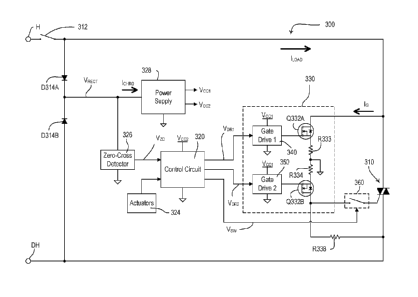
[0050] Fig. 3 is a simplified schematic diagram of an example dimmer
switch 300 (e.g., the
dimmer switch 100 shown in Fig. 1 and/or the dimmer switch 200 shown in Fig.
2). The dimmer
switch 300 may comprise a thyristor, e.g., a triac 310. The triac 310 may
comprise first and second
main terminals coupled between a hot terminal H and a dimmed hot terminal DH
and a gate terminal
configured to receive a control signal (e.g., a gate current) for rendering
the triac conductive. The
hot terminal H may receive a hot voltage VH from an AC power source (e.g., the
AC power source
105). The triac 310 may be rendered conductive to generate a phase-control
voltage Vpc at the
dimmed-hot terminal and conduct a load current 'LOAD through an electrical
load (e.g., the LED
driver 102 shown in Fig. 1) for controlling of the amount of power delivered
to the electrical load.
[0051] The dimmer switch 300 may comprise a control circuit 320, e.g., a
digital control
circuit having a processor, such as, a microprocessor, a programmable logic
device (PLD), a
microcontroller, an application specific integrated circuit (ASIC), a field-
programmable gate
array (FPGA), or any suitable controller or processing device. The control
circuit 320 may be
responsive to actuators 324 (e.g., the rocker switch 116 and/or the intensity
adjustment actuator 118).
The digital control circuit of the dimmer switch 300 may enable the dimmer
switch to offer
advanced features and functionality to a user. For example, the user may be
able to adjust the
features and functionality of the dimmer switch 300 using an advanced
programming mode. The
control circuit 320 may be operable to enter the advanced programming mode in
response to one or
more actuations of the actuators 324. For example, the user may adjust the low-
end intensity LLE
and the high-end intensity LHE between which the control circuit 320 may
control the target
intensity L I RG1 of the LED light source 104. A dimmer switch having an
advanced programming
mode is described in greater detail in commonly-assigned U.S. Patent No.
7,190,125, issued
March 13, 2007, entitled PROGRAMMABLE WALLBOX DIMMER. In addition, the
operation of
the dimmer switch 300 may be configured using an external programming device
(such as a smart
phone, a tablet, or a laptop) as described in greater detail in commonly-
assigned U.S. Patent
Application Publication No. 2013/0026947, published January 31, 2013, entitled
METHOD OF
PROGRAMMING A LOAD CONTROL DEVICE USING A SMART PHONE.
CA 2996603 2019-06-05
CA 02996603 2018-02-23
WO 2017/041011 PCT/US2016/050227
- 17 -
[0052] The dimmer switch 300 may comprise a power supply 328 configured to
conduct a
charging current IcHRG through the electrical load (e.g., the LED driver 102)
for generating a first DC
supply voltage Vcci (e.g., approximately 8 volts) and a second DC supply
voltage Vcc2 (e.g.,
approximately 4 volts). The power supply 328 may be used to power, for
example, at least the
microprocessor 320 (e.g., via the second DC supply voltage Vcc2). Both of the
first and second DC
supply voltages Vcci, Vcc2 may be referenced to a circuit common and the power
supply 328 may
conduct the charging current IcHRG through circuit common. For example, the
power supply 328
may comprise a resistor-zener power supply for generating the first DC supply
voltage Vcci and a
high-efficiency switching power supply for generating the second DC supply
voltage Vcc2. The
power supply 328 may comprise one or more linear regulators, or other suitable
power supply, in
addition to any combination of linear regulators, switching power supplies,
and resistor-zener power
supplies. As shown in Fig. 3, the dimmer switch 300 may not comprise a neutral
terminal (e.g., to
be coupled to the neutral side N of the AC power source 105). As such, the
power supply 328 may
be configured to conduct the charging current IcHRG through the electrical
load. The power supply
328 may also be configured to not conduct the charging current IcHRG through
an earth ground
connection, as shown in Fig. 3.
[0053] The dimmer switch 300 may comprise a zero-cross detection circuit
326 that may
generate a zero-cross signal Vzc that indicates the zero-crossings of the AC
line voltage. Since the
dimmer switch 300 may not comprise a neutral connection and/or an earth ground
connection, the
zero-cross detection circuit 326 may be coupled between the hot terminal H and
the dimmed-hot
terminal DH, and may be responsive to a dimmer voltage VDIM (e.g., the voltage
across the dimmer
switch 300). The zero-cross detection circuit 326 may be configured to drive
the zero-cross signal
Vzc low towards circuit common when the magnitude of the dimmer voltage VDIM
rises above a
zero-cross threshold (e.g., approximately 30 volts) during the positive half-
cycles of the AC power
source 105. The control circuit 320 may receive the zero-cross signal Vzc and
may determine when
to render the triac 310 conductive during a half cycle of the AC power source
based on the
indications of the zero-crossings from the zero-cross signal. The control
circuit 320 may sample the
zero-cross signal Vzc during a zero-cross window, e.g., once every line cycle
(or every half cycle),
to look for an indication of a zero-crossing. For example, a falling edge of
the zero-cross signal Vzc
at the beginning of the positive half-cycles may indicate a zero-crossing of
the AC power source
-18-
105. The control circuit 320 may determine when to sample the zero-cross
signal Vzc during a zero-
cross window based on a previous zero-crossing time (e.g., approximately the
period of one line
cycle from the previous zero-crossing time). If the control circuit 320 does
not detect an indication
of a zero-crossing in a predetermined number of sequential line cycles (e.g.,
approximately three line
cycles), the control circuit 320 may reset.
[0054] Although not shown in Fig. 3, the dimmer switch 300 may comprise a
neutral
terminal (not shown) adapted to be coupled to a neutral connection (e.g., the
neutral side of the AC
power source 105). For example, the power supply 328 may be coupled between
the hot terminal H
and the neutral terminal, such that the power supply may not conduct the
charging current 1CHRG
through the electrical load. In addition, the dimmer switch 300 may comprise a
neutral terminal
zero-cross detection circuit (not shown) that may be coupled between the hot
terminal H and the
neutral terminal for generating a zero-cross signal indicating the zero-
crossings of the AC power
source 105.
[0055] If the dimmer switch 300 comprises a neutral terminal, the dimmer
switch 300 may
comprise either or both of the zero-cross detection circuit 326 (e.g., coupled
between the hot
terminal and the dimmed hot terminal) and the neutral terminal zero-cross
detection circuit (e.g.,
coupled between the hot terminal H and the neutral terminal). The dimmer
switch 300 may be
configured to determine if the neutral terminal is electrically connected to
the neutral side of the AC
power source 105 in response to the neutral terminal zero-cross detection
circuit. The dimmer
switch 300 may be configured to operate in a two-wire mode in which the
control circuit 320 is
responsive to the zero-cross circuit 326 coupled between the hot terminal H
and the dimmed hot
terminal DH, and in a three-wire mode in which the control circuit is
responsive to the neutral
terminal zero-cross detection circuit (e.g., in response to determining that
the neutral terminal is
connected to the neutral side of the AC power source 105). An example of a
dimmer switch
configured to operate in two-wire and three-wire modes of operation is
described in greater detail in
commonly-assigned U.S. Patent No. 7,859,815, issued December 28, 2010,
entitled ELECTRONIC
CONTROL SYSTEMS AND METHODS.
[0056] The dimmer switch 300 may comprise an earth ground terminal (not
shown) adapted
to be coupled to an earth ground connection. For example, the power supply 328
may be coupled
CA 2996603 2019-06-05
CA 02996603 2018-02-23
WO 2017/041011 PCT/US2016/050227
- 19 -
between the hot terminal H and the earth ground terminal for leaking at least
a portion of the
charging current ICHRG through the earth ground connection (e.g., the power
supply may not
conduct any of the charging current IcHRG through the electrical load). In
addition, the dimmer
switch 300 may comprise an earth ground terminal zero-cross detection circuit
(not shown) that may
be coupled between the hot terminal H and the earth ground terminal for
generating a zero-cross
signal indicating the zero-crossings of the AC power source 105.
[0057] The dimmer switch 300 may comprise a gate coupling circuit 330 and a
controllable
switching circuit 360 electrically coupled in series between the control
circuit 320 and the gate
terminal of the triac 310. The gate coupling circuit 330 and the controllable
switching circuit 360
may operate as a gate current path (e.g., the gate current path 220 shown in
Fig. 2) for conducting
pulses of gate current IG through the gate terminal of the triac 310 to render
the triac conductive.
[00581 The gate coupling circuit 330 may comprise a voltage-controlled
controllably
conductive device, such as two MOS-gated transistors (e.g., FETs Q332A, Q332B)
coupled in
anti-series connection between the gate of the triac 310 and a first one of
the main terminals of the
triac 310 (e.g., the hot terminal H of the dimmer switch). The FETs Q332A,
Q332B may comprise
MOSFETs or any suitable voltage-controlled semiconductor switches, such as,
for example, IGBTs.
The sources of the FETs Q332A, Q332B may be coupled together through two
source
resistors R333, R334 (e.g., each having a resistance of approximately 10 S2).
The source
resistors R333, R334 may operate to limit the magnitude of the gate current IG
conducted through the
gate of the triac 310 to a maximum gate current (e.g., approximately 0.6 amp).
The junction of the
source resistors R333, R334 may provide the circuit common for the power
supply 328 to allow the
power supply to conduct the charging current IcHRG through the electrical
load.
[0059] The gate coupling circuit 330 may comprise first and second gate
drive circuits 340,
350 that allow for control (e.g., independent control) of the FETs Q332A,
Q332B. The control
circuit 320 may generate two drive signals VDR1, VDR2 that are received by the
respective gate drive
circuits 340, 350 for rendering the respective FETs Q332A, Q332B conductive
and non-conductive,
such that the triac 310 may be rendered conductive to conduct the load current
LOAD to the electrical
load (e.g., when the controllable switching circuit 360 is also rendered
conductive). For example,
the control circuit 320 may drive the respective drive signals VDR1, VDR2 high
towards the second
supply voltage Vcc2 to render the respective gate drive circuits 340, 350
conductive. The dimmer
CA 02996603 2018-02-23
WO 2017/041011 PCT/US2016/050227
- 20 -
switch 300 may further comprise a full-wave rectifier bridge that may include
the body diodes of the
FETs Q332A, Q332B and the diodes D314A, D314B, and may generate the rectified
voltage VRECT
that is received by the control circuit 320 and the power supply 328.
[0060] The control circuit 320 may generate a switch control signal Vsw for
rendering the
controllable switching circuit 360 conductive and non-conductive. When the
controllable switching
circuit 360 is conductive, the control circuit 320 may render the FETs Q332A,
Q332B conductive to
allow the gate coupling circuit 330 to conduct a pulse of gate current IG
through the gate terminal of
the triac 310 to render the triac conductive, e.g., at the firing time each
half cycle. When operating
in the first gate drive mode (e.g., the pulse gate drive mode), the control
circuit 320 may control the
drive signals VDR1, VDR2 to render both of the FETs Q332A, Q332B non-
conductive (e.g., after the
short pulse time period TPULSE) so that the gate current IG may not be
conducted through the gate
terminal of the triac 310.
[0061] The dimmer switch 300 may comprise a resistor R338, which may have a
resistance
of, for example, approximately 90.9 Q and may be coupled between the gate and
a second one of the
main terminals of the triac 310 (e.g., to the dimmed hot terminal DH of the
dimmer switch). The
gate coupling circuit 330 and the resistor R338 may operate as part of an
alternate load current path
(e.g., the alternate load current path 230 shown in Fig. 2). When operating in
the second gate drive
mode (e.g., the constant gate drive mode), the control circuit 320 may be
configured to control the
FETs Q332A, Q332B of the gate coupling circuit 330 to conduct the load current
koAD to the
electrical load via the alternate load current path after the triac 310
becomes non-conductive and
before the end of the present half cycle. For example, the control circuit 320
may be configured to
render the controllable switching circuit 360 non-conductive (e.g., at the
time TNON-CON in the
present half cycle) to disconnect the gate terminal of the triac 310 from the
FETs Q332A, Q332B of
the gate coupling circuit 330 before the end of each half cycle of the AC line
voltage, such that the
triac 310 is able to commutate off before the end of the half cycle. Between
the time the triac 310
commutates off and the end of the present half cycle, the control circuit 320
may be configured to
conduct the load current Koko to the electrical load via the alternate load
current path.
[0062] Fig. 4 is a simplified schematic diagram of a portion of the dimmer
switch 300
showing the first and second gate drive circuits 340, 350 and the controllable
switching circuit 360
in greater detail. The first gate drive circuit 340 may comprise an NPN
bipolar junction
CA 02996603 2018-02-23
WO 2017/041011 PCT/US2016/050227
-21 -
transistor Q341 having a base that receives the first drive voltage VDR1 via a
resistor R342 (e.g.,
having a resistance of approximately 200 kf2). The collector of the transistor
Q341 may be coupled
to the first DC supply voltage Vcci through a resistor R343 (e.g., having a
resistance of
approximately 200 kn), and to the base of another NPN bipolar junction
transistor Q344. The
collector-emitter junction of the transistor Q344 may be coupled in series
with a diode D345 and the
collector-emitter junction of another NPN bipolar junction transistor Q346.
The base of the
transistor Q346 may be coupled to the first DC supply voltage Vcci through a
resistor R347 (e.g.,
having a resistance of approximately 200 kK2) and to the collector of the
transistor Q346. The
junction of the transistor Q346 and the diode D345 may be coupled to the gate
of the first
FET Q332A through a gate resistor R348 (e.g., having a resistance of
approximately 47 K2).
[0063] When the magnitude of the first drive voltage VDR1 is low (e.g., at
approximately
circuit common), the transistor Q341 may be non-conductive, such that the base
of the
transistor Q345 may be pulled up towards the first DC supply voltage Vcci.
Accordingly, the
transistor Q345 may be rendered conductive, pulling the base of the transistor
Q346 and the gate of
the first FET Q332A down towards circuit common, such that the FET may be non-
conductive.
However, when the first drive voltage VDR1 is high (e.g., at approximately the
first DC supply
voltage Vcci), the transistor Q341 may become conductive, such that the
transistor Q344 may be
rendered non-conductive. Thus, the transistor Q346 may become conductive and
the gate of the first
FET Q332A may be driven up towards the first DC supply voltage Vcci, such that
the FET may be
rendered conductive. The second gate drive circuit 350 may have a similar
structure and operation
(e.g., an identical structure and operation) for rendering the second FET
Q332B conductive and non-
conductive in response to the second drive voltage VDR2.
[0064] The controllable switching circuit 360 may be coupled between the
anti-series-
connected FETs Q332A, Q332B and the gate terminal of the triac 310 and may be
responsive to the
switch control signal Vsw from the control circuit 320. The gate terminal of
the triac 310 may be
coupled to one of the main teiininals of the triac 310 through the parallel
combination of a capacitor
C370 (e.g., having a capacitance of approximately 0.1 [if) and a resistor R372
(e.g., having a
resistance of approximately 47 K2). The controllable switching circuit 360 may
include a full-wave
rectifier bridge comprising four diodes D361-D364. The AC terminals of the
rectifier bridge may be
coupled in series with the gate terminal of the triac 310, while an NPN
bipolar junction transistor
CA 02996603 2018-02-23
WO 2017/041011 PCT/US2016/050227
- 22 -
Q365 may be coupled across the DC terminals of the rectifier bridge. The
controllable switching
circuit 360 may comprise an optocoupler U366 having an output phototransistor
that may be coupled
in series with a resistor R367 across the DC terminals of the bridge. For
example, the resistor R367
may have a resistance of approximately 150 ka The switch control signal Vsw
may be coupled to
the input photodiode of the optocoupler U366 via a resistor R368 (e.g., having
a resistance of
approximately 10 kf2). When the switch control signal Vsw is low, the output
phototransistor of the
optocoupler U366 may be non-conductive, such that the transistor Q365 may be
non-conductive
(e.g., the controllable switching circuit 360 may be non-conductive). However,
when the switch
control-voltage Vsw is high, the output phototransistor of the optocoupler
U366 may be rendered
conductive, such that the transistor Q365 may be conductive (e.g., the
controllable switching
circuit 360 may be conductive and the gate of the triac 310 may receive
current conducted by the
anti-series-connected FETs Q332A, Q332B).
[0065] The control circuit 320 may be configured to operate in a pulse gate
drive mode to
render both the gate coupling circuit 330 and the controllable switching
circuit 360 conductive for a
short pulse time period TPULSE after the firing time in one or more half
cycles (e.g., in each half
cycle) of the AC power source. The gate coupling circuit 330 and the
controllable switching circuit
360 may form part of a gate current path (e.g., the gate current path 220
shown in Fig. 2) between
the control circuit 330 and the triac 310. By rendering both the gate coupling
circuit 330 and the
controllable switching circuit 360 conductive, the control circuit 320 may
render the gate current
path conductive. For example, the control circuit 320 may control the switch
control signal Vsw to
render the controllable switching circuit 360 conductive and may control the
first and second drive
voltages VDR1, VDR2 to enable the FETs Q332A, Q332B to conduct a pulse of gate
current IG via the
gate current path and through the gate terminal of the triac 310 to render the
triac 310 conductive.
After the triac 310 has been rendered conductive, the control circuit 320 may
control the switch
control signal Vsw to render the controllable switching circuit 360 non-
conductive (e.g., after the
short pulse time period TPULSE) and thus to render the gate current path non-
conductive. As a result,
the gate current IG may cease to be conducted through the gate terminal of the
triac 310 (e.g., after
the short pulse time period TPULSE).
[0066] The control circuit 320 may be configured to operate in a constant
gate drive mode
during one or more half cycles of the AC power source to provide constant gate
drive (e.g., gate
CA 02996603 2018-02-23
WO 2017/041011 PCT/US2016/050227
- 23 -
current) to the triac 310. The control circuit 320 may control the gate
coupling circuit 330 and the
controllable switching circuit 360 (e.g., and thus to control the gate current
path) to conduct gate
current IG (e.g., at the firing time of a half cycle) through the gate
terminal of the triac 310 to render
the triac 310 conductive. The control circuit may then maintain the gate
current path conductive for
the remainder of the half cycle (e.g., for a substantial portion of the
remainder of the half cycle) so
that further pulses of gate current IG may be conducted through the gate
terminal of the triac 310.
Accordingly, the triac 310 may be operable to remain conductive (e.g, due to
the gate current IG)
independent of the magnitude of the load current koAD conducted through the
dimmer switch 300
and the electrical load (e.g., the LED driver 102).
[0067] Fig. 5 shows example waveforms illustrating the operation of the
dimmer switch 300
when the control circuit 320 is operating in the constant gate drive mode. The
control circuit 320
may be configured to determine the zero-crossing of the AC line voltage at
time ti in response to the
zero-cross voltage Vzc generated by the zero-cross detection circuit 326. At
the beginning of each
half cycle (e.g., while operating in the constant gate drive mode), the
control circuit 320 may be
configured to render the FETs Q332A, Q332B non-conductive, such that the first
FET Q332A
blocks current during the positive half cycles and the second FET Q332B blocks
current during the
negative half cycles. The control circuit 320 may be configured to drive both
of the drive
voltages VDR1, VDR2 high at the same time, such that the FETs Q332A, Q332B are
operable to
conduct the gate current IG through the gate of the triac 310 (e.g., when the
controllable switching
circuit 360 is also rendered conductive) to render the triac conductive at the
firing time (e.g., at time
t3 as shown in Fig. 5).
[0068] The control circuit 320 may be configured to render the FETs Q332A,
Q332B
conductive for different periods of time or durations. For instance, during a
half cycle, the control
circuit 320 may be configured to control one of the FETs Q332A, Q332B to be
conductive for a first
drive time period TDR1 and to drive the other FET to be conductive for a
second (and longer) drive
time period TDR2. As shown in Fig. 5, during a positive half cycle, the
control circuit 320 may be
configured to drive the second drive voltage VDR2 low at time t5 before the
end of the half cycle (e.g.,
at time t6 in Fig. 5), such that the second FET Q332B may be non-conductive
and ready to block
current at the beginning of a subsequent half cycle (e.g., a negative half
cycle). After the second
drive voltage VDR2 is driven low at time t5, the second FET Q332B may be
configured to conduct
CA 02996603 2018-02-23
WO 2017/041011 PCT/US2016/050227
- 24 -
current through its body diode until the end of the positive half cycle (e.g.,
to maintain the gate
current path conductive). The control circuit 320 may be configured to drive
the first drive voltage
VDR1 low after the end of the positive half cycle at time t7, such that the
first FET Q332A may
remain conductive until the end of the present positive half cycle. Similarly,
during a negative half
cycle, the control circuit 320 may be configured to drive the first drive
voltage VDR1 low before the
end of the negative half cycle and drive the second drive voltage VDR2 low
after the end of the
negative half cycle.
[0069] The control circuit 320 may be configured to drive the switch
control signal Vsw high
(e.g., at time t2 as shown in Fig. 5) in a half cycle to cause the
controllable switching circuit 360 to
become conductive at the same time or prior to rendering the FETs Q332A, Q332B
conductive, for
example, approximately 40 psec before the time t3 when the FETs are rendered
conductive. If the
FETs Q332A, Q332B allow the gate terminal of the triac 310 to conduct the gate
current IQ too close
to the end of the half cycle, the triac 310 may mistakenly be rendered
conductive at the beginning of
the next half cycle, which could cause the triac to be conductive for the
entire next half cycle (e.g., to
thus cause flicker in the LED light source 104). Therefore, the control
circuit 320 may be
configured to drive the switch control signal Vsw low to cause the
controllable switching circuit 360
to become non-conductive before the end of the present half cycle (e.g., at
time Li in Fig. 5). For
example, the control circuit 320 may be configured to drive the switch control
signal Vsw low at
time t4 approximately 600-1000 [tsec before the end of the half cycle (which
occurs at time t6 in
Fig. 5), such that the switch control signal Vsw is high for a switch control
time period Tsw in the
half cycle. Since the controllable switching circuit 360 may be controlled to
be non-conductive
before the end of the half cycle (e.g., to thus prevent further pulses of gate
current IG from being
conducted via the gate current path), the triac 310 may be able to commutate
off when the magnitude
of the load current UAL) drops below the rated holding current of the triac.
The triac 310 may not
become conductive again during the present half cycle (e.g., due to the lack
of a gate drive) and may
remain non-conductive at the beginning of the next half cycle. If the
electrical load (e.g., the LED
driver 102) needs to conduct current after the triac 310 commutates off, the
FETs Q332A, Q332B
may be configured to conduct the load current koAD (e.g., via the alternate
load current path
described herein) . Accordingly, the dimmer switch 300 may be configured to
conduct the load
CA 02996603 2018-02-23
WO 2017/041011 PCT/US2016/050227
- 25 -
current UAL) through the electrical load independent of the rated holding
current of the triac 310 and
without driving the triac 310 to be conductive too close to the next half
cycle.
[0070] Thus, as described herein, the gate current IG may be able to be
conducted through the
gate current path comprising the controllable switching circuit 360 and the
FETs Q332A, Q332B of
the gate coupling circuit 330 between the firing time t3 and a transition time
before the end of the
half cycle (e.g., at time t4 when the controllable switching circuit 360 is
rendered non-conductive).
The load current IwAn may be able to be conducted through the alternate load
current path
comprising the resistor R338 and the FETs Q332A, Q332B of the gate coupling
circuit 330 when the
triac 310 commutates off near the end of the half cycle (e.g., after the
transition time t4 when the
controllable switching circuit 360 is rendered non-conductive) until the end
of the half cycle.
[0071] The control circuit 320 may be configured to operate in one or the
other of the pulse
gate drive mode and the constant gate drive mode. For example, the control
circuit 320 may be
configured to operate in the constant gate drive mode when the dimmer switch
300 is in a steady
state condition, when the control circuit 320 is turning the LED light source
104 on or off, and when
the target intensity LIRGI is dynamically changing (e.g., in response to an
actuation of the intensity
adjustment actuator 118).
[0072] For some high-efficiency lighting loads (e.g., particular models
and/or products by
particular manufacturers), turning on the high-efficiency lighting loads using
the constant gate drive
mode may cause fault conditions. For example, the control circuit 320 may not
be able to determine
accurate zero-crossing information from the zero-cross voltage Vzc generated
by the zero-cross
detection circuit 326 for some high-efficiency lighting loads while turning on
the high-efficiency
lighting loads using the constant gate drive mode. Accordingly, the control
circuit 320 may not
receive indications of zero-crossings of the AC line voltage when zero-
crossings are expected, and
may reset after detecting a predetermined number of missed zero-crossings.
[0073] Fig. 6 shows example waveforms illustrating the operation of the
dimmer switch 300
when turning on an example LED light source using the constant gate drive
mode. Fig. 6 illustrates
the dimmer voltage VDIM (e.g., the voltage across the dimmer switch 300) and
the zero-cross
signal Vzc that is generated by the zero-cross detection circuit 326 from the
dimmer voltage VDTM.
The control circuit 320 may be configured to detect indications of zero-
crossings in response to the
CA 02996603 2018-02-23
WO 2017/041011 PCT/US2016/050227
- 26 -
falling edges of the zero-cross signal Vzc. The control circuit 320 may sample
the zero-cross
signal Vzc during zero-cross windows 400 near the beginning of each line
cycle.
[0074] The high-efficiency lighting load 101 may draw (e.g., leak) current
through the
dimmer switch 300 when the LED light source 104 is off. This leakage current
may charge the bus
capacitor Caus of the high-efficiency lighting load 101 and cause the voltage
across the
high-efficiency lighting load (e.g., the phase-control voltage) to increase in
magnitude over one or
more half cycles even though the triac 310 is non-conductive (as shown in the
first three line cycles
of Fig. 6). As a result, the voltage across the dimmer switch 300 (e.g., a
dimmer voltage \Timm) may
decrease in peak magnitude in each of the one or more half cycles, which may
cause the indications
of the zero-crossings (e.g., the falling edges of the zero-cross signal Vzc)
and the zero-cross
windows 400 to move later into a subsequent line cycle (as shown in Fig. 6).
This may lead to
incorrect detection of the zero-crossings and timing errors when rendering the
triac 310 conductive.
For example, when the control circuit 320 controls the drive signals VDRI,
VDR2 to render the triac
conductive at time ti, the indication of the zero-crossing may be so late in
the half cycle that the
control circuit 320 may keep the gate coupling circuit 330 and the
controllable switching circuit 360
conductive into the next half cycle (as shown at time t2). This may cause the
triac 310 to be rendered
into full conduction (e.g., the phase-control voltage is equal to
approximately the AC line voltage
and the dimmer voltage VDIM is approximately zero volts) and remain fully
conductive in one or
more subsequent half cycles. The control circuit 320 may then not detect
indications of
zero-crossings during the next several (e.g., three) zero-cross windows 400
and may reset (e.g., at
time t3). This may cause undesirable flickering and/or blinking in the LED
light source 104.
[0075] If the control circuit 320 controls the gate coupling circuit 330
and the controllable
switching circuit 360 (e.g., to thus control the gate current path) using the
pulse gate drive mode, the
controllable switching circuit 360 (e.g., and thus the gate current path) may
be rendered non-
conductive long before the end of a half cycle and thus the triac 310 may not
be rendered into full
conduction in a subsequent half cycle. Therefore, the control circuit 320 may
be configured to
operate in the pulse gate drive mode when turning on the LED light source 104
and in the constant
gate drive mode in the steady state condition (e.g., after the LED light
source has been turned on).
[0076] Fig. 7 shows example waveforms illustrating the operation of the
dimmer switch 300
when turning on an example LED light source using the pulse gate drive mode.
The control
CA 02996603 2018-02-23
WO 2017/041011 PCT/US2016/050227
- 27 -
circuit 320 may be configured to control the gate coupling circuit 330 and the
controllable switching
circuit 360 (e.g., to thus control the gate current path) using the pulse gate
drive mode for a turn-on
time period TruRN-ox (which may comprise one or more half cycles of the AC
power source), before
changing to the constant gate drive mode during steady state conditions. The
control circuit 320
may be configured to control the drive signals VDR1, VDR2 to render the gate
coupling circuit 330
conductive at the firing time of a half cycle (e.g., at time ti in Fig. 7). At
or before time ti, the
control circuit may control the switch control signal Vsw to render the
controllable switching circuit
360 conductive such that when the gate coupling circuit 330 becomes conductive
at ti, the triac may
be rendered conductive (e.g., via gate current To conducted over the gate
current path and into the
gate terminal of the triac).
[0077] The control circuit 320 may be configured to render the controllable
switching
circuit 360 non-conductive (e.g., to thus render the gate current path non-
conductive) after a pulse
time period TPULSE from the firing time by rendering the controllable
switching circuit 360 non-
conductive (e.g., at time t2 in Fig. 7) The control circuit 320 may render the
controllable switching
circuit 360 non-conductive by driving the switch control signal Vsw low (e.g.,
at time t2). The
control circuit 320 may control the drive signals VDR1, VDR2 to maintain the
gate coupling circuit 330
conductive for a period of time before the end of the present half-cycle and
after the controllable
switching circuit 360 has been rendered non-conductive. This way, the load
current koAD may be
conducted through the alternate load current path described herein while the
gate coupling circuit
330 remains conductive. Alternatively, the control circuit 320 may drive the
drive signals VDR1,
VDR2 low at the same time it drives the switch control signal Vsw low (e.g.,
at time t2 of the present
half-cycle). This way, the load current LOAD may not be conducted through the
alternate load
current path during the remainder of present half-cycle.
[0078] The control circuit 320 may adjust the length of the pulse time
period TPULSE over one
or more line cycles (or half cycles) during the turn-on time period TTURN-ON.
The one or more line
cycles (or half cycles) may be consecutive. For example, the control circuit
320 may set the pulse
time period TPULSE equal to a minimum pulse time period TPULSE-MIN (e.g.,
between times ti and t2
with a value equal to approximately 100 [tsec) during a first half cycle of
the turn-on time
period TTuRN-ox. The control circuit 320 may increase the pulse time period
TPULSE by a
predetermined increment TiNc (e.g., approximately 20 lasec) during a
subsequent half cycle (e.g.,
CA 02996603 2018-02-23
WO 2017/041011 PCT/US2016/050227
- 28 -
between times t3 and t4). The control circuit 320 may increase the pulse time
period TpuLsE by a
same increment (e.g., approximately 20 litsec) or by varying amounts during
consecutive line cycles
(or half cycles) or during selected line cycles (which may not be consecutive)
until the pulse time
period is equal to a maximum pulse time period TPULSE-MAX. The amount of
increment (same or
varying) be applied in a line cycle may be predetermined. The maximum pulse
time period TPULSE-
MAX may be equal to the length of the time period during which the gate
current path remains
conductive in a constant gate drive mode half cycle. The length of the pulse
time period may be
dependent upon what is required to drive the triac 310 using the constant gate
drive mode to achieve
a target intensity LTRGT of the light source (e.g., dependent upon a present
firing time of the constant
gate drive mode). As such, the maximum pulse time period TPULSE-MAX may be
dependent upon the
target intensity LTRGT to which the control circuit 320 is turning on the LED
light source 104.
Accordingly, at the end of the turn-on time period TTURN-ON, the control
circuit 320 may smoothly
transition into the constant gate drive mode (e.g., at time t5 in Fig. 7) to
achieve the target
intensity LTRGT. For example, the maximum pulse time period TPULSE-MAX may be
approximately 0.5
msec when the target intensity LTRGT is at the low-end intensity LLE and
approximately 5.5 msec
when the target intensity L MGT is at the high-end intensity LHE. In examples,
the turn-on time period
TTuRN-ON may range from approximately 20 line cycles (at low-end) and
approximately 270 line
cycles (at high-end).
[0079] The control circuit 320 may maintain the pulse time period TPULSE
constant during the
turn-on time period TTuRN-ON. In such cases, the control circuit 320 may
adjust the pulse time
period TPULSE at the end of the turn-on time period TTURN-ON (and/or the
beginning of the constant
gate drive mode), so that the pulse time period TPULSE may be approximately
equal to the gate pulse
time period required to drive the triac 310 to achieve the target intensity
Liam- using the constant
gate drive mode.
[0080] Fig. 8 shows an example procedure 800 for operating a dimmer switch
(e.g., the
dimmer switch 300 described herein). Using the dimmer switch 300 as an
example, at 802, the
control circuit 320 of the dimmer switch may detect a zero-crossing of the AC
power source (e.g.,
via the zero-cross detection circuit 326). The control circuit may be
configured to fire the triac 310
at a firing time of a present half-cycle in response to detecting the zero-
crossing. At or before the
firing time, the control circuit may, at 804, drive the switch control signal
Vsw high. At the firing
CA 02996603 2018-02-23
WO 2017/041011 PCT/US2016/050227
- 29 -
time, the control circuit 320 may drive both of the drive voltages \TWO, VDR2
high (e.g., as shown at
806) to render the triac 310 conductive (e.g., via gate current IG conducted
over the gate current path
and into the gate terminal of the triac).
[0081] At 808, the control circuit 320 may drive the switch control signal
Vsw low before the
end of the present half-cycle. During the constant gate drive mode, the
control circuit 320 may drive
the switch control signal Vsw low close to the end of each half-cycle (e.g.,
approximately
600-1000 pec before the end of the half cycle as shown at time t4 in Fig. 5).
During the pulse gate
drive mode, the control circuit 320 may drive the switch control signal Vsw
low shortly after driving
the drive voltages VDRI, VDR2 high (e.g., at the end of the minimum pulse time
period TPULSE-MIN as
shown at time t2 in Fig. 7). When the control circuit 320 is turning on the
lighting load, the time at
which the control circuit may drive the switch control signal Vsw low may
vary, for example,
dependent upon where the present half-cycle is in the turn-on time period
TTURN-ON (which may
comprise one or more half cycles of the AC power source). For example, during
a first half-cycle of
the turn-on time period TTURN-ON, the control circuit 320 may drive the switch
control signal Vsw
low after the pulse time period TPULSE-MIN from the firing time (e.g., the
time at which the control
circuit drives the drive voltages VDRI, VDR2 high). In one or more subsequent
half-cycles, the control
circuit 320 may be configured to increase (e.g., gradually widen) the length
of the pulse time period.
For instance, in a subsequent half-cycle, the control circuit 320 may drive
the switch control
signal Vsw low at a time after the firing time, e.g., at the end of the pulse
time period TPULSE. For
example, the control circuit 320 may increase the pulse time period TPULSE by
the predetermined
increment TINc (e.g., approximately 20 ttsec) each line cycle during the turn-
on time
period TTURN-ON, e.g.,
TPULSE = TPULSE-MIN (N
where N is a number that represents the current line cycle during the turn-on
time period TTURN-ON
and increases by one each line cycle (e.g., until the light source enters a
steady state and/or the pulse
time period reaches a maximum length TPULSE-MAX).
[0082] At 810, the control circuit 320 may determine whether the present
half-cycle of the
AC power source is a positive or a negative half-cycle. If the present half-
cycle is a positive half-
cycle, the control circuit 320 may drive the drive voltage VDR2 low before the
end of the half-cycle
(e.g., as shown at 812), and drive the drive voltage VDR1 low after the end of
the half-cycle (e.g., as
CA 02996603 2018-02-23
WO 2017/041011 PCT/US2016/050227
-30 -
shown at 814). Otherwise (e.g., if the present half-cycle is a negative half-
cycle), the control circuit
320 may drive the drive voltage VDR1 low before the end of the half-cycle
(e.g., as shown at 816),
and drive the drive voltage VDR2 low after the end of the half-cycle (e.g., as
shown at 818).
[0083] The control circuit 320 may be configured to first attempt to turn
on the LED light
source 104 using the constant gate drive mode, detect a fault condition (e.g.,
that the control
circuit 320 resets), and subsequently attempt to turn on the LED light source
104 using the pulse gate
drive mode in response to detecting the fault condition. If the control
circuit 320 is able to turn on
the LED light source 104 using the constant gate drive mode or the pulse gate
drive mode without
detecting fault conditions, the control circuit may be configured to store an
indication of the suitable
gate drive mode in memory for turning on the LED light source, such that the
control circuit may use
that gate drive mode at a subsequent time when the control circuit is
attempting to turn on the LED
light source 104. If the control circuit 320 is not able to turn on the LED
light source 104 using
either of the constant gate drive mode and the pulse gate drive mode, the
control circuit 320 may
attempt to turn on the LED light source using another mode of operation or
another start-up routine
as described herein.
[0084] More generally, a control circuit as described herein (e.g., the
control circuit 320)
may be configured to attempt one of a plurality of start-up routines for
turning on the light source,
detect a fault condition, and subsequently attempt another one of the
plurality of start-up routines
until a suitable start-up routine is identified that can turn on the light
source without fault conditions.
The start-up routines may each comprise one or more actions taken by the
control circuit to turn on
an electrical load. These may include operating the control circuit in a
particular operation mode
(e.g., the pulse gate drive mode or constant gate drive mode described
herein), operating the control
circuit in a combination of operation modes (e.g., with or without a
particular order), or performing
the functions of a particular operation mode in different manners.
[0085] For example, a start-up routine may comprise turning on the light
source using the
constant drive mode as described herein. A start-up routine may comprise
controlling one or more
components of the dimmer switch 300 in a particular manner such that a gate
current may be
conducted through the gate terminal of the thyristor for only a pulse time
period after the firing time
during a half-cycle of the AC power source (e.g., as described in association
with Fig. 7 and with the
pulse gate drive mode). For example, one start-up routine may comprise
gradually increasing the
CA 02996603 2018-02-23
WO 2017/041011 PCT/US2016/050227
-31 -
pulse time period TPULSE, in one or more half-cycles during the turn-on time
period TTURN-ON, while
another start-up routine may comprise keeping the pulse time period TpuLsE
constant during the turn-
on time period TTuRN-ON and increasing the pulse time period TpuLsE at the end
of the turn-on time
period TTURN-ON. To further illustrate, one start-up routine may comprise
driving the switch control
signal Vsw low (e.g., at t2 of Fig. 7) before driving the drive voltages VDR1,
VDR2 low (e.g., such that
an alternate load current path may be maintained around the gate current path)
while another start-up
routine may comprise driving the switch control signal Vsw low at the same
time of driving the drive
voltages VDR1, VDR2 low (e.g., such that an alternate load current path around
the gate current path
may be rendered non-conductive at the same time the gate current path is
rendered non-conductive).
[0086] Fig. 9 shows an example procedure 900 for operating a dimmer switch
(e.g., the
dimmer switches 300 described herein) when turning on a light source. Using
the dimmer
switch 300 as an example, at 902, the control circuit 320 may attempt a first
start-up routine (e.g., by
using the constant gate drive mode described herein) to turn on the light
source. At 904, the control
circuit 320 may determine whether the dimmer has reset (e.g., which may
represent a fault
condition) during the first start-up routine. If no reset has occurred (e.g.,
the light source has not
entered a fault condition), the control circuit 320 may continue performing
the current start-up
routine (and subsequent routines for operating the light source in a steady
state) at 916. For
example, if the control circuit 320 does not detect a fault condition while
turning on the light source
using the constant gate drive mode, the control circuit 320 may complete the
start-up procedure and
continue to operate the light source in a steady state with a steady state
operation mode (e.g., which
may also be the constant gate drive mode).
[0087] If a reset is detected at 904, the control circuit 320 may attempt a
second start-up
routine, at 906, to turn on the light source. The second start-up routine may
comprise, for example,
controlling one or more components of the dimmer switch 300 in a particular
manner (e.g., as
described herein) such that a gate current may be conducted through the gate
terminal of the thyristor
for only a pulse time period after the firing time during a half-cycle of the
AC power source (e.g., as
provided by the gate drive mode described herein). At 908, the control circuit
320 may determine
whether the dimmer has reset (e.g., which may represent a fault condition)
during the second start-up
routine. If no reset has occurred (e.g., the light source has not entered a
fault condition), the control
circuit 320 may continue performing the current start-up routine (and
subsequent routines for
CA 02996603 2018-02-23
WO 2017/041011 PCT/US2016/050227
-32 -
operating the light source in a steady state) at 916. For example, if the
control circuit 320 does not
detect a fault condition while turning on the light source using the second
start-up routine, the
control circuit 320 may complete the start-up procedure with the current start-
up routine, and
continue to operate the light source in a steady state with a steady state
operation mode (e.g., which
may be the constant gate drive mode).
[0088] If a reset is detected at 908, the control circuit 320 may attempt a
third start-up
routine, at 910, to turn on the light source. For example, the third start-up
routine may comprise
controlling one or more components of the dimmer switch 300 in a different
manner than the second
start-up routine such that a gate current may be conducted through the gate
terminal of the thyristor
for only a pulse time period after the firing time during a half-cycle of the
AC power source (e.g., as
provided by the gate drive mode described herein). For instance, the third
start-up routine may
comprise setting the pulse time period to a first value (e.g., to TPULSE-MIN)
in a first half-cycle of the
AC power source, and then increasing (e.g., gradually increasing) the pulse
time period in one or
more subsequent half-cycles (e.g., consecutive half-cycles) of the AC power
source. At 912, the
control circuit 320 may determine whether the dimmer has reset (e.g., which
may represent a fault
condition) during the third start-up routine. If no reset has occurred (e.g.,
the light source has not
entered a fault condition), the control circuit 320 may continue performing
the current start-up
routine (and subsequent routines for operating the light source in a steady
state) at 916. If a reset is
detected at 912, the control circuit 320 may revert to performing the first
start-up routine, and the
actions described herein may be repeated.
[00891 Although three start-up routines are shown as an example in Fig. 9,
it should be noted
that the scope of the disclosure is not limited by such an example. The
control circuit 320 may be
configured to choose from more or fewer than three start-up routines to start
up the electrical load.
For example, when more than three start-up routines are available, the control
circuit 320 may
perform the additional start-up routines after 914 in a similar manner as that
illustrated in association
with 904-914.
[0090] If the dimmer switch 300 has a neutral terminal and the control
circuit 320 determines
that the neutral terminal is connected to the neutral side of the AC power
source 105, the control
circuit may be configured to operate in the pulse gate drive mode in multiple
situations (e.g.,
including at all times). For example, the control circuit 320 may be
configured to operate in the
CA 02996603 2018-02-23
WO 2017/041011 PCT/1JS2016/050227
-33 -
pulse gate drive mode when the dimmer switch 300 is in the steady state
condition, when the control
circuit 320 is presently turning the LED light source 104 on or off, and when
the target
intensity LTRGT is dynamically changing. If the control circuit 320 determines
that the neutral
terminal is not connected to the neutral side of the AC power source 105, the
control circuit may be
configured to operate in the constant gate drive mode both when turning on the
electrical load and
when in the steady state condition (e.g., including at all times), or to
operate in the pulse gate drive
mode when turning on the LED light source 104 and then operating in the
constant gate drive mode
when in the steady state condition.
[0091] The control circuit 320 may be configured to operate in one of the
constant gate drive
mode and the pulse gate drive mode in response to a user input received, for
example, from
actuations of the actuators 324 during the advanced programming mode and/or
from an external
programming device (such as a smart phone, a tablet, or a laptop).
[00921 Fig. 10 is a simplified block diagram of another load control
device, e.g., a dimmer
switch 500, which may be deployed as the dimmer switch 100 of Fig. I or the
dimmer switch 200 of
Fig. 2. The dimmer switch 500 may comprise a full-wave rectifier bridge 514
(including four
diodes D514A, D514B, D514C, D514D) that has AC terminals electrically coupled
in series
between a hot terminal H and a dimmed hot terminal DH, and DC terminals for
providing a rectified
voltage VRECT to a control circuit 530 (e.g., a digital control circuit). The
control circuit 530 may
comprise a processor, e.g., a microprocessor, a programmable logic device
(PLD), a microcontroller,
an application specific integrated circuit (ASIC), a field-programmable gate
array (FPGA), or any
suitable controller or processing device. The dimmer switch 500 may comprise a
gate coupling
circuit 550 electrically coupled in series between the control circuit 530 and
the gate terminal of the
triac 510. The gate coupling circuit 550 may operate as part of a gate current
path (e.g., the gate
current path 220 shown in Fig. 2) for conducting pulses of gate current IG
through the gate terminal
of the triac 510 to render the triac conductive.
[0093] The gate coupling circuit 550 may comprise a voltage-controlled
controllably
conductive device, such as a single MOS-gated transistor (e.g., a FET Q552)
inside of a full-wave
rectifier bridge that includes diodes D556A-D556D (as well as the diode
D514D). The FET Q552
may be coupled across the DC tet tninals of the full-wave rectifier bridge,
while the AC terminals are
coupled between the hot terminal H and the gate of the triac 510 The gate
coupling circuit 550 may
CA 02996603 2018-02-23
WO 2017/041011 PCT/US2016/050227
-34 -
receive a drive voltage VDR from the control circuit 530, and the drive
voltage VDR may be coupled
to the gate of the FET Q552 via a gate drive circuit 560. When the FET Q552 is
rendered
conductive, a pulse of gate current IG may be conducted through the FET Q552,
the diodes D556A,
D556D, and the gate terminal of the triac 510 during positive half cycles of
the AC power source to
render the triac conductive. During negative half cycles of the AC power
source, a pulse of gate
current IG may be conducted through the gate terminal of the triac 510, the
FET Q552, and the
diodes D556B, D556C and the diode D514D. While not shown as such in Fig. 10,
the diode D556B
may comprise four diodes coupled in series to ensure that the diode D556D is
forward biased during
the positive half cycles.
[0094] The dimmer switch 500 may comprises one or more actuators 536 (e.g.,
the rocker
switch 116 and/or the intensity adjustment actuator 118) for receiving user
inputs and a zero-cross
detection circuit 534 for generating a zero-cross voltage Vzc representative
of the zero-crossing of
the AC line voltage VAC. The control circuit 530 may be configured to render
the triac 510
conductive in response to the zero-cross detection circuit 534 and/or the
actuators 536. The dimmer
switch 500 may further comprise a resistor 554 (e.g., having a resistance of
approximately 30-47 Q)
coupled between the gate of the triac 510 and the dimmed hot terminal DH
(e.g., the second main
load terminal of the triac 510).
[0095] The dimmer switch 500 may comprise a power supply 520 for generating
a first DC
supply voltage Vcci (e.g., approximately 2.8 volts) for powering the control
circuit 530 and a
boosting power supply, e.g., a boost converter 528, which may receive the
first DC supply voltage
Vcci and generate a second boosted DC supply voltage Vcc2 (e.g., approximately
15 volts) for
driving the FET Q552 of the gate coupling circuit 550.
[0096] The dimmer switch 500 may further comprise a controllable switching
circuit 580.
The controllable switching circuit 580 may be coupled to the DC terminals of
the full-wave rectifier
bridge 514, such that the controllable switching circuit 580 may be coupled in
parallel electrical
connection with the triac 510. The controllable switching circuit 580 may
operate as an alternate
load current path (e.g., similar to the alternate load current path 230 shown
in Fig. 2) to allow the
load current kaki) to flow through the electrical load when the triac is non-
conductive. The control
circuit 530 may generate a load-current-path control signal VLcp for rendering
the controllable
switching circuit 580 (and thus the gate current path) conductive and non-
conductive For example,
CA 02996603 2018-02-23
WO 2017/041011 PCT/US2016/050227
-35 -
the controllable switching circuit 580 may comprise a field-effect transistor
(FET) or other suitable
semiconductor switch or switching circuit coupled across the DC terminals of
the full-wave rectifier
bridge 514. The controllable switching circuit 580 may comprise a drive
circuit (not shown) for
providing the second DC supply voltage Vcc2 to the gate of the FET for
rendering the FET
conductive, e.g., in response to the load-current-path control signal VLcp.
The controllable switching
circuit 580 may comprise a bidirectional semiconductor switch (such as a triac
or two FETs in anti-
series connection) or other suitable switching circuit coupled across the AC
terminals of the full-
wave rectifier bridge 514.
[0097] The control circuit 530 may be configured to operate in a pulse gate
drive mode to
render the gate coupling circuit 550 (and thus the gate current path)
conductive for a short pulse time
period TPULSE after the firing time in a half cycle. The control circuit 530
may control the drive
voltage VDR to render the gate coupling circuit 550 conductive to allow the
FET Q552 to conduct a
pulse of gate current IG through the gate terminal of the triac 510 to render
the triac conductive.
After the triac 510 has been rendered conductive, the control circuit 530 may
control the drive
voltage VDR to render the gate coupling circuit 550 (and thus the gate current
path) non-conductive
(e.g., after the short pulse time period TpuLsE) during the remainder of the
half cycle (e.g., during a
substantial portion of the remainder of the half cycle).
[0098] The control circuit 530 may be configured to operate in a constant
gate drive mode to
provide constant gate drive to the triac 510. The control circuit 530 may
control the drive voltage
VDR to render the gate coupling circuit 550 (and thus the gate current path)
conductive at the firing
time of a half cycle, such that gate current IG may be conducted through the
gate terminal of the triac
510 to thus render the triac 510 conductive at the firing time. The control
circuit may then maintain
the gate coupling circuit 550 (and thus the gate current path) conductive for
the remainder of the half
cycle (e.g., for a substantial portion of the remainder of the half cycle)
after the firing time.
Accordingly, the triac 510 may be operable to remain conductive (e.g., due to
the gate current IG)
independent of the magnitude of the load current koAD conducted through the
dimmer switch 500
and the electrical load (e.g., the LED driver 102).
[0099] Fig. 11 shows example waveforms illustrating the operation of the
dimmer
switch 500 of Fig. 10 when operating in the constant gate drive mode. The
control circuit 530 may
drive the drive voltage VDR high towards the first DC supply voltage Vcci to
render the gate
CA 02996603 2018-02-23
WO 2017/041011 PCT/US2016/050227
-36 -
coupling circuit 580 (and thus the gate current path) conductive at the firing
time (e.g., at time ti in
Fig. 11) of one or more half cycles. The gate current IG may then be conducted
through the gate of
the triac to render the triac 510 conductive. The control circuit 530 may
maintain the drive voltage
VDR high to keep the gate coupling circuit 550 (and thus the gate current
path) conductive after the
firing time ti until a transition time (e.g., at time t2) before the next zero-
crossing (e.g.,
approximately 600 microseconds before the next zero-crossing). Since the gate
coupling circuit 550
is rendered non-conductive before the end of the half cycle, the triac 510 may
be able to commutate
off when the magnitude of the load current koAD drops below the rated holding
current of the triac.
The triac 510 may not be rendered conductive again during the present half
cycle and may remain
non-conductive at the beginning of the next half cycle.
[00100] The control circuit 530 may drive the load current path control
signal VLcp high to
render the controllable switching circuit 580 conductive at approximately the
transition time t2, such
that the controllable switching circuit is able to conduct the load current
koAD if the triac 510
commutates off before the end of the half cycle. For example, the control
circuit 530 may drive the
load current path control signal VL.cp high before driving the drive voltage
VDR low to render the gate
coupling circuit 550 non-conductive (e.g., approximately 10 microseconds
before driving the drive
voltage VDR 1010 so that the controllable switching circuit 580 may be
rendered conductive at or
before the time when the triac 510 commutates off. The control circuit 530 may
then drive the load
current path control signal VLcp low to render the controllable switching
circuit 580 non-conductive
at the end of the half cycle (e.g., at time t3 in Fig. 11).
[00101] The control circuit 530 may be configured to operate in the pulse
gate drive mode or
the constant gate drive mode based on various factors including, for example,
user inputs or the
operational state of the electrical load. The control circuit 530 may be
configured to operate in one
of the constant gate drive mode or the pulse gate drive mode in response to
one or more user inputs
received, for example, from actuations of the actuators 536 during the
advanced programming mode
and/or from an external programming device (such as a smart phone, a tablet,
or a laptop).
[00102] The control circuit 530 may be configured to operate in the pulse
gate drive mode
when turning on the electrical load and in the constant gate drive mode in
steady state conditions
(e.g., in a similar manner as the control circuit 320 of the dimmer switch
300). The control
circuit 530 may be configured to control the gate coupling circuit 550 (and
thus the gate current
CA 02996603 2018-02-23
WO 2017/041011 PCT/US2016/050227
-37 -
path) using the pulse gate drive mode for a turn-on time period TruRN-ON,
before changing to the
constant gate drive mode during steady state conditions. The control circuit
530 may be configured
to control the drive signal VDR to render the gate coupling circuit 550
conductive at the firing time
and thus render the triac 510 conductive (e.g., by conducting gate current IG
via the gate current path
and through the gate terminal of the triac). The control circuit 530 may be
configured to render the
gate coupling circuit 550 (and thus the gate current path) non-conductive
after the pulse time
period TPULSE from the firing time by rendering the controllable switching
circuit 580
non-conductive The control circuit 530 may adjust the length of the pulse time
period TPULSE over
one or more line cycles (or half cycles) during the turn-on time period TTURN-
ON. The one or more
line cycles (or half cycles) may be consecutive. For example, during the turn-
on time period TTURN-
ON, the control circuit 530 may be configured to increase the pulse time
period TPULSE by a
predetermined increment TINC (e.g., approximately 20 psec) during consecutive
line cycles from a
minimum pulse time period TPULSE-MIN (e.g., approximately 100 usec) to a
maximum pulse time
period TPULSE-MAX (which may range, for example, from approximately 0.5 msec
at low-end to
approximately 5.5 msec at high-end). The length of the turn-on time period
TFURN-ON may be
dependent upon a target intensity LTRGT and may range, for example, from
approximately 20 line
cycles (at low-end) to approximately 270 line cycles (at high-end). The
maximum pulse time
period TPULSE-MAX may be equal to the length of the time period during which
the gate current path
remains conductive in a constant gate drive mode half cycle. The length of the
time period may be
dependent upon what is required to drive the triac 510 using the constant gate
drive mode to achieve
a target intensity LTRGT of the light source (e.g., dependent upon a present
firing time of the constant
gate drive mode). The maximum pulse time period TPULSE-MAX may thus be
dependent upon the
target intensity LTRGT to which the control circuit 530 is turning on the LED
light source 104.
Accordingly, at the end of the turn-on time period TTURN-ON, the control
circuit 530 may smoothly
transition into the constant gate drive mode to achieve the target intensity
LTRGT.
[00103] The control circuit 530 may maintain the pulse time period TPULSE
constant during the
turn-on time period TTURN-ON. In such cases, the control circuit 530 may
adjust the pulse time
period TPULSE at the end of the turn-on time period TTURN-ON (and/or the
beginning of the constant
gate drive mode), so that the pulse time period TPULSE may be approximately
equal to the gate pulse
CA 02996603 2018-02-23
WO 2017/041011 PCT/US2016/050227
-38 -
time period required to drive the triac 510 to achieve the target intensity
LTRGr using the constant
gate drive mode.
[00104] The control circuit 530 may be configured to perform at least a
subset of the
procedure illustrated by and described in association with Fig. 8.
[00105] The control circuit 530 may be configured to first attempt to turn
on the LED light
source 104 using the constant gate drive mode, detect a fault condition (e.g.,
that the control
circuit 530 reset), and subsequently attempt to turn on the LED light source
104 using the pulse gate
drive mode in response to detecting the fault condition. If the control
circuit 530 is able to turn on
the LED light source 104 using the constant gate drive mode or the pulse gate
drive mode without
detecting fault conditions, the control circuit may be configured to store an
indication of the suitable
gate drive mode in memory for turning on the LED light source 104, such that
the control circuit
may use that gate drive mode whenever the control circuit is attempting to
turn on the LED light
source 104. If the control circuit 530 is not able to turn on the LED light
source 104 using either of
the constant gate drive mode and the pulse gate drive mode, the control
circuit 530 may attempt to
turn on the LED light source using another mode of operation. More generally,
the control circuit
530 may turn on the light source by performing a procedure similar to that
illustrated in and
described in association with Fig. 9.
[00106] If the dimmer switch 500 has a neutral terminal and the control
circuit 530 deteimines
that the neutral terminal is connected to the neutral side of the AC power
source 105, the control
circuit may be configured to operate in the pulse gate drive mode in multiple
situations (e.g.,
including at all times). If the control circuit 530 determines that the
neutral terminal is not connected
to the neutral side of the AC power source 105, the control circuit may be
configured to operate in
the constant gate drive mode both when turning on the electrical load and when
in the steady state
condition (e.g., including at all times), or to operate in the pulse gate
drive mode when turning on the
LED light source 104 and then operating in the constant gate drive mode when
in the steady state
condition.