Note: Descriptions are shown in the official language in which they were submitted.
CA 02996898 2018-02-26
DESCRIPTION
THERMOELECTRIC CONVERSION ELEMENT AND
THERMOELECTRIC CONVERSION MODULE
TECHNICAL FIELD
[0001]
The present invention relates to thermoelectric conversion elements and
thermoelectric modules.
BACKGROUND ART
[0002]
Thermoelectric conversion elements are known as clean energy
conversion elements without the use of petroleum or ozone, and have been
desired to be made more efficient, larger in area and thinner in recent years.
For example, power generation elements using the Seebeck effect
(thermoelectric
conversion power generation elements) and cooling/heating elements using the
Peltier effect (Peltier elements) have been under development.
[0003]
The structure and the principle of such thermoelectric conversion
elements are described. FIG.3 is a conception diagram for illustrating a
structure of a conventional thermoelectric conversion element.
A conventional thermoelectric conversion element 100 as shown in FIG.3
is basically called a n-type thermoelectric conversion element, and composed
of
a plurality of electrodes opposed (metal electrodes) 120, 121, and 180; and a
block body 130 made of an n-type thermoelectric semiconductor and a block
body 131 made of a p-type thermoelectric semiconductor which are disposed
1
CA 02996898 2018-02-26
between the electrodes. The block bodies 130 and 131 are electrically
connected to each other by the electrode 180 at their ends on one side
(junction
end), and a block body of an n-type thermoelectric conversion semiconductor
and a block body of a p-type thermoelectric conversion semiconductor are
connected in series. The block bodies 130 and 131 are connected to the
electrodes 120 and 121, respectively, at their ends on the other side.
[0004]
In this configuration, if the temperature of the electrode 180 is made high
and the temperature of the opposite electrode 120, 121 is made low, a
temperature difference is provided therebetween, thermal energy is converted
into electric energy by the Seebeck effect. Also, for example, by applying a
direct
current voltage between the electrode 180 and the electrodes 120, 121, and by
passing a current from the electrode 120 in the direction of the electrode 121
via
the electrode 180, the electrode 180 acts as an endothermic working electrode,
the electrodes 120, 121 act as heat radiation working electrodes, and electric
energy is converted into thermal energy by the Peltier effect.
[00051
Here, the endothermic energy in the case where the conventional
thermoelectric conversion element is used as a Peltier element is discussed.
The endothermic energy Q on an upper side of the electrode 180 is represented
by the following equation (1):
Q = QP QR (1),
wherein Qp is an amount of Peltier endotherm, QR is an amount of Joule heat,
and QK is an amount of heat conduction (see FIG.3).
Currently, the element structure of a practical thermoelectric
conversion element has a block shape of a cross-sectional area S at about
several
2
CA 02996898 2018-02-26
mm2 and a length L at about several mm. Multiple block bodies having such a
shape are connected in series to be modularized, and a thermoelectric
conversion
element (Peltier element) whose heat absorption area (cooling area) is
expanded
by modularization has been put to practical use. However, such a n-type
thermoelectric conversion element is about several mm in length L, so that
radiation heat from the heat source directly affects the electrode of the low-
temperature portion, therefore it is difficult to ensure the temperature
difference
between the electrodes. In addition, the shape is nonflexible, it is difficult
to bring
the electrode portions into close contact with the heat source or the cooling
source, therefore there is a problem that it is difficult to secure a
temperature
difference between the electrodes.
[00061
To overcome the above problems, recently it has got actively developing a
sheet-type thermoelectric conversion element, that is an element of forming
thermoelectric conversion materials on a flexible insulating sheet and forming
both a high-temperature electrode and a low-temperature electrode at each end
surface of the sheet as shown in FIG.2 (For example, see Non-Patent Document
1). Such a sheet-type thermoelectric conversion element has the structure to
be
able to take a certain distance between the high-temperature electrode and the
low-temperature electrode in a plane, therefore the low-temperature electrode
can avoid an influence of direct radiant heat from the heat source, as a
result
there is an advantage that it gets easy to secure a temperature difference
between
electrodes. Furthermore, the use of flexible sheets allows the electrode
portion
adhere to heat/cold sources, therefore it also gets easy to ensure the
temperature
difference between electrodes.
3
CA 02996898 2018-02-26
RELATED ART DOCUMENTS
[0007]
Non-Patent Document 1:Yoshiyuki Nonoguchi, Kenji Ohashi, Rui
Kanazawa, Koji Ashiba, Kenji Hata, Tetsuya Nakagawa, Chihaya Adachi,
Tomoaki Tanase and Tsuyoshi Kawai, "Systematic Conversion of Single Walled
Carbon Nanotubes into n-type Thermoelectric Materials by Molecular Dopants",
Scientific Reports, Published 26 November 2013, Volume 3, Article number:
3344, doi:10.1038/srep03344.
SUMMARY OF THE INVENTION
PROBLEMS TO BE SOLVED BY THE INVENTION
[0008]
However, in the sheet type thermoelectric conversion element, due to the
element structure in which the thickness of the thermoelectric conversion
material layer is thin and the distance between the high temperature electrode
and the low temperature electrode is long, there is a problem that the
internal
resistance of the thermoelectric conversion material layer becomes high,
therefore, it is difficult to obtain a large output.
Further, conventional thermoelectric conversion elements have been
developed by concurrently letting three characteristics have in thermoelectric
conversion materials, which are high Seebeck coefficient (thermoelectric
force),
high electric conductivity, and low thermal conductivity. However, it is
difficult
to obtain a material that simultaneously satisfies these three properties, in
particular, if a thermoelectric conversion material having high electric
conductivity is used to improve the internal resistance of the thermoelectric
conversion material layer, the Seebeck coefficient decreases(See Fig.4), as a
result, there is a problem that it is impossible to obtain a large output.
4
CA 02996898 2018-02-26
MEANS FOR SOLVING THE PROBLEMS
[0009]
According to the present invention, a thermoelectric conversion element
may comprise at least a charge transport layer, a thermoelectric conversion
material layer and electrodes, wherein the charge transport layer comprises
graphite treated to dope charge-donating materials so that the graphite has an
n-type semiconductor property, or graphite treated to dope charge-accepting
materials so that the graphite has a p-type semiconductor property.
Further, according to the present invention, an n-type thermoelectric
conversion element may comprise at least an n-type charge transport layer, n-
type thermoelectric conversion material layers and electrodes, wherein the n-
type charge transport layer comprises graphite treated to dope charge-donating
materials so that the graphite has an n-type semiconductor property, and the n-
type thermoelectric conversion material layers are formed on the both ends of
the n-type charge transport layer, and the electrodes are formed on top of the
n-
type thermoelectric conversion material layers.
Further, according to the present invention, a p-type thermoelectric
conversion element may comprise at least a p-type charge transport layer, p-
type
thermoelectric conversion material layers and electrodes, wherein the p-type
charge transport layer comprises graphite treated to dope charge-accepting
materials so that the graphite has a p-type semiconductor property, and the p-
type thermoelectric conversion material layers are formed on the both ends of
the p-type charge transport layer, and the electrodes are formed on top of the
p-
type thermoelectric conversion material layers.
Further, according to the present invention, the charge-donating
materials in the thermoelectric conversion element may comprise at least one
5
CA 02996898 2018-02-26
of the group consisting of tetrathiafulvalene(TTF), tetramethyl-
tetrathiafulvalene(TMTTF), bis-ethylenedithio-tetrathiafulvalene(BEDT-TTF),
Tetraselenafulvalene(TSF), triphenylphosphine(TPP),
trimethoxyphenylphosphine(Me0-TPP),
trifluoride-triphenylphosphine(F-TPP), diphenylphosphine(DPP), bis-
diphenylphosphino-ethane(DPPE),
bis-diphenylpho sphino-propane(DPPP), amines, polyamines,
polyethyleneimine, sodium-carbonate, lithium-carbonate, potassium-
carbonate, Cu-phthalocyanine, Zn-phthalocyanine and the like, derivatives
thereof.
Further, according to the present invention, the charge-accepting
materials in the thermoelectric conversion element may comprise at least one
of the group consisting of tetracyanoquinodimethane(TCNQ), tetrafluoro-
tetracyanoquinodirnethane(TCNQF4), dicyclopentyldimethoxysilane-
dicyanobenzoquinone(DDQ), trinitrofluorenone(TNF), dinitro-fluorenone(DNF),
carbazole, 9H-carbazole-4o1, 2-hydroxy-9H-carbazole, phenyl-boronic-acid,
pyridine, quinoline, imidazole, triphenylamine and the like, and derivatives
thereof.
Further, according to the present invention, the thermoelectric
conversion material layers in the thermoelectric conversion element may
comprise at least one of carbon nanotubes, Bi-Te based compounds, oxides, or
combinations of these materials.
Further, according to the present invention, a thermoelectric conversion
module may be constituted by connecting at least one of the above-mentioned
n-type thermoelectric conversion elements and at least one of the above-
6
mentioned p-type thermoelectric conversion elements in series or in parallel,
or
in a combination of series and parallel.
Further, in the present invention, the thermoelectric conversion element
has further an insulating substrate, wherein, the insulating substrate may be
a
composite substrate formed by joining two pieces of a second substrates to
both
ends of a first substrate, and the second substrate may be made of insulating
materials having higher thermal conductivity than that of the first substrate,
wherein, the charge transport layer is formed on the insulating substrate, and
the thermoelectric conversion material layers are formed on the doped layer at
both ends of the charge transport layer.
Further, in the present invention, thermoelectric conversion material
layers may be formed on the doped layer at both ends of the charge transport
layer and passivation film may be formed on the exposed portion of the doped
layer of the central part of the charge transport layer where the
thermoelectric
conversion material layer is not formed.
Further, according to the present invention, a thermoelectric conversion
module may be constituted by connecting at least two or more of the above-
mentioned thermoelectric conversion elements in series or in parallel or in a
combination of series and parallel.
In a broad aspect, moreover, the present invention provides:
(1) A
thermoelectric conversion element comprises at least a charge
transport layer and thermoelectric conversion material layers and electrodes,
wherein the charge transport layer comprises a surface of a graphite treated
to
dope charge-donating material so that the surface has an n-type semiconductor
property, or a surface of a graphite treated to dope charge-accepting material
so
that the surface has a p-type semiconductor property, wherein the thermal
7
CA 2996898 2019-04-17
conductivity in the in-plane direction of the doped surface of the graphite is
reduced by doping the charge-donating material or the charge-accepting
material and wherein charge carriers are transported in the in-plane direction
of
the doped surface.
(2) The thermoelectric conversion element according to (1), wherein
the charge transport layer comprises a surface of a graphite treated to dope
charge-donating material, and wherein n-type thermoelectric conversion
material layers are formed at the doped surface of the both ends of the n-type
charge transport layer, and the electrodes are formed on the upper parts of
the
thermoelectric conversion material layers.
(3) The thermoelectric conversion element according to (1), wherein
the charge transport layer comprises a surface of a graphite treated to dope
charge-accepting material, and wherein p-type thermoelectric conversion
material layers are formed at the doped surface of the both ends of the p-type
charge transport layer, and the electrodes are formed on the upper parts of
the
thermoelectric conversion material layers.
(4) The thermoelectric conversion element according to (1), wherein
the charge-donating material comprises at least one of the group consisting of
tetrathiafulvalene (TTF), tetramethyl-tetrathiafulvalene (TMTTF), bis-
ethylenedithio-tetrathiafulvalene (BEDT-TTF), tetraselenafulvalene (TSF),
triphenylphosphine (TPP), trimethoxyphenylphosphine (Me0-TPP), trifluoride-
triphenylphosphine (F-TPP), diphenylphosphine (DPP), bis-diphenylphosphino-
ethane (D PPE), bis-diphenylphosphino-propane (D PPP), amines, polyamines,
polyethyleneimine, sodium-carbonate, lithium-carbonate, potassium-
carbonate, Cu-phthalocyanine, and Zn-phthalocyanine.
7a
CA 2996898 2019-04-17
(5) The thermoelectric conversion element according to (1), wherein
the charge-accepting material comprises at least one of the group consisting
of
tetracyanoquinodimethane (TCNQ), tetrafluoro-tetracyanoquinodimethane
(TCNQF4), dicyclopentyldimethoxysilane-dicyanobenzoquinone (DD Q),
trinitrofluorenone (TNF), dinitro-fluorenone (DNF), carbazole, 9H-carbazole-
4o1,
2-hydroxy-9H-carbazole, phenyl-boronic-acid, pyridine, quinoline, imidazole,
and triphenylamine.
(6) The thermoelectric conversion element according to (1), wherein
the thermoelectric conversion material layers comprise at least one of the
group
consisting of carbon nanotubes, Bi-Te based compounds, and oxides.
(7) The thermoelectric conversion element according to (1), wherein
the thermoelectric conversion element further comprises an insulating
substrate,
wherein, the insulating substrate is a composite substrate formed by joining
two
pieces of a second substrate one by one to both ends of a first substrate, and
wherein the second substrate is made of insulating material having higher
thermal conductivity than that of the first substrate.
(8) The thermoelectric conversion element according to (1), wherein
the thermoelectric conversion material layers are formed on both ends of the
charge transport layer, and a passivation film is formed on the exposed
portion
of the doped layer of the central part of the charge transport layer where the
thermoelectric conversion material layer is not formed.
(9) A thermoelectric conversion module constituted by connecting a
plurality of the thermoelectric conversion elements according to (2) and a
plurality of the thermoelectric conversion elements according to (3).
EFFECTS OF THE INVENTION
[0010]
7b
CA 2996898 2019-04-17
The thermoelectric conversion element of the present invention is
characterized in using the graphite surface as the charge transfer layer which
is
doped with either charge-donating materials or charge-accepting materials so
that the graphite surface has either an n-type or a p-type semiconductor
property. Electric conductivity of the graphite surface having semiconductor
7c
CA 2996898 2019-04-17
CA 02996898 2018-02-26
property is more than 100 times high as compared with that of conventional
thermoelectric conversion materials. Also, it hardly causes heat
generating/absorbing even if it contacts with thermoelectric conversion
materials. Further, the graphite surface doped with charge-donating materials
or charge-accepting materials has lower thermal conductivity.
The present invention, by using the graphite surface pretreated so that
the graphite surface has an n-type or a p-type semiconductor property as a
charge transport layer, it is possible to lower the internal resistance of the
sheet-
type thermoelectric conversion element. The sheet type thermoelectric
conversion element has a structure having a certain distance in a plane
between
the high temperature electrode and the low temperature electrode, therefore
there is an advantage that a large temperature difference can be secured
between
the electrodes. Further, materials having high Seebeck coefficient can be
selected
as n-type or p-type thermoelectric conversion materials formed on the both end
surfaces of the charge transport layer. By providing a charge transport layer
to
thermoelectric conversion materials, it becomes possible to use the
thermoelectric conversion materials which have not been used so much up to
now because of their very low electric conductivity even though the Seebeck
coefficient is high. As a result, it has got possible to provide a
thermoelectric
conversion element of the large output unprecedented.
Further, in the present invention, a passivation film is formed on the
portion exposed the doped layer of the charge transport layer, thus it is
possible
to provide a time stable thermoelectric conversion element.
Further, in the present invention, by using an insulating substrate in
which an insulating material having high thermal conductivity and an
insulating
material having low thermal conductivity are combined, it can provide an
8
CA 02996898 2018-02-26
excellent thermoelectric conversion module which one end portion of the
laminated modules functions effectively as a heating/high-temperature section
and another end portion of the laminated modules functions effectively as a
cooling/low-temperature section.
The present invention provides a thermoelectric conversion element and
a thermoelectric conversion module having such excellent thermoelectric
performances, and provides a clean new energy conversion technology.
BRIEF DESCRIPTION OF THE DRAWINGS
[0011]
FIG.1 is a top view, and a sectional view of a thermoelectric conversion
element A according to Embodiment 1 of the present invention.
FIG.2 is a top view, and a sectional view of a thermoelectric conversion
element according to Comparative Embodiment 1 of the present invention.
FIG.3 is a conception diagram for illustrating a structure of a
conventional thermoelectric conversion element.
FIG.4 is a schematic diagram for showing thermoelectric performance
characteristics (room temperature) of thermoelectric conversion materials.
FIG.5 is an explanatory diagram for showing an example of production
processes of a thermoelectric conversion module according to Embodiment 2 of
the present invention. (1) shows the first layer (process 1) of the
thermoelectric
conversion module, (2) shows the second layer (process 2) of the
thermoelectric
conversion module, (3) shows the third layer (process 3) of the thermoelectric
conversion module, (4) shows the forth layer (process 4) of the thermoelectric
conversion module.
FIG.6 is a schematic diagram of a thermoelectric conversion module
according to Embodiment 3 of the present invention. (1) shows a perspective
view
9
CA 02996898 2018-02-26
of the thermoelectric conversion module,(2) shows a sectional view taken along
line E-E of the thermoelectric conversion module in (1).
FIG.7 is an explanatory view for showing a connection example between
a thermoelectric conversion module and an output measuring device according
to Embodiment 2 or 3 of the present invention.
MODE FOR CARRYING OUT THE INVENTION
[0012]
[Thermoelectric Conversion Element of Present Invention]
Graphite has anisotropy with respect to electric conduction
characteristics, and the sheet manufactured from natural graphite has electric
conductivities in the in-plane direction at approximately 2,000 to 10,000S/cm,
an electric conductivity in the thickness direction at approximately 1S/cm. A
graphite sheet obtained by graphitization of a sheet of a polymer such as
polyimide has electric conductivities in the in-plane direction at
approximately
10000 to 25000 S/cm and an electric conductivity in a thickness direction at
approximately 5 S/cm. And, the thermoelectric conversion material has an
electric conductivity of approximately 500 to 1000 S/cm, therefore either of
the
graphite sheets can be used as an effective charge transport layer by using
the
high electric conductivity in the in-plane direction of the graphite.
[0013]
Upon use of graphite as a charge transport layer, the graphite is
pretreated so that the graphite has n-type or p-type semiconductor property in
order to perform carrier transport without energy loss between the graphite
and
the thermoelectric conversion materials. As methods for pretreatment, it is
able
to use methods for transforming carbon nanotubes or graphene into an n-type
or a p-type semiconductor.
CA 02996898 2018-02-26
As methods for transforming the graphite into n-type semiconductor, it
is able to use a method of heat-treating the graphite under potassium
atmosphere, or a method of doping charge-donating materials and the like.
As the charge-donating materials for doping, it can be used at least one
of the group consisting of tetrathiafulvalene(TTF),tetramethyl-
tetrathiafulvalene(TMTTF),bis-ethylenedithio-tetrathiafulvalene(BEDT-TTF),
Tetraselenafulvalene(TSF),triphenylphosphine(TPP),trimethoxyphenylphosphine
(Me0-TPP),
trifluoride-triphenylphosphine(F-TPP), diphenylphosphine(DPP), bis-
diphenylphosphino-ethane(DPPE),
bis-diphenylphosphino-propane(DPPP), amines, polyamines,
polyethyleneimine, sodium-carbonate, lithium-carbonate, potassium-
carbonate, Cu-phthalocyanine, Zn-phthalocyanine and the like, and derivatives
thereof.
As methods for transforming the graphite into p-type semiconductor, it is
able to use a method of introducing lattice defects into the graphite, or a
method
of doping charge-accepting materials and the like.
As the charge-accepting materials for doping, it can be used at least one
of the group consisting of tetracyanoquinodimethane (TCNQ), tetrafluoro-
tetracyanoquinodimethane(TCNQF4), dicyclopentyldimethoxysilane-
dicyanobenzoquinone(DDQ), trinitrofluorenone(TNF), dinitro-fluorenone(DNF),
carbazole, 9H-carbazole-4o1, 2-hydroxy-9H-carbazole, phenyl-boronic-acid,
pyridine, quinoline, imidazole, triphenylamine and the like, and derivatives
thereof.
Further, it was found that the thermal conductivity of the graphite
surface is greatly reduced by doping with charge-donating materials or charge-
11
CA 02996898 2018-02-26
accepting materials. The following is known, phonon propagation of graphite
propagates two-dimensionally on the graphite surface, unlike the case where
phonons propagate in bulk solid three-dimensionally, therefore, by injecting
lattice defects into the graphite surface, the average free path of the
phonons
gets equal to the distance between the lattice defects, as a result, the
thermal
conductivity is greatly reduced. The cause of this reduction of the thermal
conductivity in the present invention is considered that the doping elements
instead of the lattice defects play role to inhibit the two-dimensional
propagation
of phonons.
[0014]
(1)
As the thermoelectric conversion materials in the present invention, it
can be used at least one of the group consisting of carbon nanotubes, Bi-Te
based compounds, or oxides.
For the formation of carbon nanotubes, it is known a CVD method using
methane or acetylene as a raw material and a laser ablation method irradiating
a laser beam to graphite. In the present invention, carbon nanotubes are
prepared by filtering commercially available carbon nanotube dispersions. In
order to produce n-type carbon nanotubes, carbon nanotubes are doped with
charge-donating materials, and in order to produce p-type carbon nanotubes,
carbon nanotubes are doped with charge-accepting materials. As a doping
method, an organic solvent is prepared so as to contain a few wt% of each
dopant
of charge-donating materials or charge-accepting materials, and an amount
predetermined of carbon nanotubes is provided, and it is added to the organic
solvent, and after mixing and stirring the solvent, it is filtered, then after
putting
12
CA 02996898 2018-02-26
the filtration residue into a mold, it is heated and dried. In this manner,
the
thermoelectric conversion material layer is formed.
As the charge-donating materials for doping, it can be used at least one
of the group consisting of tetrathiafulvalene(TTF), tetramethyl-
tetrathiafulvalene (TMTTF) , bis-ethylenedithio-tetrathiafulvalene(BEDT-TTF),
Tetraselenafulvalene (TSF) , triphenylphosphine (TPP) ,
trimethoxyphenylphosphine(Me0-TPP) ,
trifluoride-triphenylpho sphine (F-TPP), diphenylphosphine(DPP), bis-
diphenylphosphino-ethane(DPPE),
bis-diphenylphosphino-propane(DPPP), amines, polyamines,
polyethyleneimine, sodium-carbonate, lithium-carbonate, potassium-
carbonate, Cu-phthalocyanine, Zn-phthalocyanine and the like, and derivatives
thereof.
As the charge-accepting materials for doping, it can be used at least one
of the group consisting of tetracyanoquinodimethane(TCNQ),
tetraflu oro-tetracyanoquinodimethane (TC NQ F4), dicyclopentyldimethoxysilane-
dicyanobenzoquinone(DDQ), trinitroflu orenone (TNF) , dinitro-fluorenone(DNF),
carbazole, 9H-carbazole-4o1, 2-hydroxy-9H-carbazole, phenyl-boronic-acid,
pyridine, quinoline, imidazole, triphenylamine and the like, and derivatives
thereof.
(2)
In general, thermoelectric performance characteristics of the
thermoelectric conversion material is represented by the product (S2o) of the
square of Seebeck coefficient (S) and electric conductivity (o), as shown in
FIG.4,
there are Bi-Te based compounds in the vicinity of the maximum value.
Examples of Bi-Te based compounds, it is preferred to use Bi-Te-Se based
13
CA 02996898 2018-02-26
compounds (n-type thermoelectric conversion material) and Bi-Te-Sbbased
compounds (p-type thermoelectric conversion material) that are superior to
thermoelectric performance characteristics in the range from room temperature
to 500 K.
Because Bi, Te, Se, Sb and the like are rare metals and expensive, there
is a problem that it is difficult to supply sufficiently to market demand.
Therefore,
in addition to the Bi-Te based compounds, we would examine to use oxide
materials which have not been much used up to now as thermoelectric
conversion materials because of their very low electric conductivity even
though
the Seebeck coefficient is high.
As the oxide materials, is not particularly limited, it is preferable to use
metal oxides such as Fe0,Fe203, Fe304, CuO, Cu2O, ZnO, Zni_xAlx0, MnO, NiO,
CoO, TiO2, SrTiO3.
In the structure of a conventional thermoelectric conversion element, the
three characteristics of high Seebeck coefficient, high electric conductivity,
and
low thermal conductivity are required for a thermoelectric conversion
material.
Therefore, it was difficult to use the oxide materials as a thermoelectric
conversion material, because the electric conductivity of those is very low in
the
range 0.5 S/cm or less even if the Seebeck coefficient of those is high in the
range
300 to 1000 p.V/ K.
However, in the thermoelectric conversion element having a charge
transport layer of the present invention, the charge transport layer made of
graphite plays a role for electrical conduction, and a sheet-type element
structure which can easily secures a temperature difference between electrodes
plays a role for heat conduction, and the thermoelectric conversion material
layer
has an advantage that only the Seebeck coefficient needs to be high.
Therefore,
14
CA 02996898 2018-02-26
it is possible to effectively use the oxide materials having high
Seebeckcoefficient,
and it is possible to improve greatly the output of the thermoelectric
conversion
element.
(3)
[Thermoelectric Conversion Module of Present Invention]
The thermoelectric conversion module of the Embodiment 2as shown in
FIG.5 in the present invention is arranged a large number of thermoelectric
conversion elements in series on an insulating substrate, wherein the
thermoelectric conversion element comprises an insulating substrate, a charge
transport layer, thermoelectric conversion material layers, and electrodes,
wherein the charge transport layer comprises either an n-type charge transport
layer treated by doping charge-donating materials into the graphite surface or
a
p-type charge transport layer treated by doping charge-accepting materials
into
the graphite surface.
As shown in FIG.5(2), a plurality of n-type charge transport layers 2N and
p-type charge transport layers 2P are alternately disposed on one side of the
insulating substrate while being spaced apart from each other at predetermined
intervals.
Next, as shown in FIG.5(3), n-type thermoelectric conversion material
layers 3N are formed on the both end surfaces of the n-type charge transport
layers 2N, and p-type thermoelectric conversion material layers 3P are formed
on the both end surfaces of the p-type charge transport layers 2P,
respectively.
Next, as shown in FIG.5(4), electrodes 4 are formed on the thermoelectric
conversion material layers in the third layer of FIG.5(3) so as to be in
contact
with both an n-type thermoelectric conversion material layer 3N and a p-type
thermoelectric conversion material layer 3P, thus it becomes a structure which
CA 02996898 2018-02-26
a plurality of n-type thermoelectric conversion material layers 3N and a
plurality
of p-type thermoelectric conversion material layers 3P are connected in
series.
Further, passivation films 8 are formed on the surface where the doped
layer is exposed, of the central portions of the n-type charge transport
layers 2N
and the p-type charge transport layers 2P where the thermoelectric conversion
material layers are not formed.
As the passivation film 8, it is preferable to use nitride film such as
silicon-nitride, aluminum-nitride, or carbide film such as silicon carbide, or
fluorine resins such as polytetrafluoroethylene, polyvinylidene fluoride,
tetrafluoroethylene-hexafluoropropylene.
(4)
As shown in FIG.6(1),(2), the thermoelectric conversion module according
to the Embodiment 3 of the present invention has a structure in which the
thermoelectric conversion modules MA, MB, MC are stacked in the thickness
.. direction and are connected electrically. In this case, since the end
portion of the
thermoelectric conversion module acts as a heating/high-temperature portion or
a cooling/low-temperature portion, it is preferable to have a good thermal
conductivity at each end portion between each of the thermoelectric conversion
module. In contrast, it is preferable to have a low thermal conductivity as
much
.. as possible between the heating/high-temperature section and the
cooling/low-
temperature section. In order to realize such a thermoelectric conversion
module
structure, it is preferable to use a composite substrate, of which both ends
are
made of insulating materials having high thermal conductivity, and of which
the
central portion is made of insulating materials having low thermal
conductivity,
as shown in FIG.5(1).
16
CA 02996898 2018-02-26
As the substrates comprising insulating materials having high thermal
conductivity, it is preferable to use ceramic substrates made of aluminum-
nitride,
silicon-carbide, alumina and the like, or insulating substrates coated with
aluminum-nitride, silicon-carbide, alumina and the like.
The FIG.6(2) shows a cross-sectional view of an end portion of the
thermoelectric conversion module using the ceramic substrate 5 as the
insulating substrate. The entire of the end portion has the structure having a
high thermal conductivity.
As the substrates comprising insulating materials having low thermal
conductivity, it is preferable to use plastic resin substrates made of
polyethylene, polypropylene, polystyrene, polyethylene terephthalate,
methacrylate resin, phenol resin, melamine resin, polyurethane, polycarbonate,
epoxy resin and the like, or composite resin substrates obtained by mixing
powder of glass fiber, silicon oxide, alumina in the plastic resin materials,
or
porous ceramic substrates such as porous silicon, porous alumina, or the like.
As shown in FIG.7, by using an insulating substrate of the present
invention, one end portion of the laminated thermoelectric conversion modules
functions effectively as a heating/high-temperature section, the other end
portion of the laminated thermoelectric conversion modules functions
effectively
as a cooling/low-temperature section, therefore excellent thermoelectric
conversion performances can be realized.
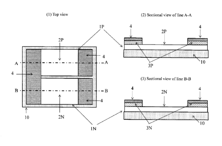
[0015]
Next, the thermoelectric conversion element according to the
Embodiment 1 is described based on FIG.1.
[Embodiment 1]
17
CA 02996898 2018-02-26
The thermoelectric conversion element A according to the Embodiment 1
is described. FIG.1 is a drawing of a thermoelectric conversion element
A.FIG.1(1) is the top view, FIG. 1(2) is the sectional view taken along the
line A-A
in FIG.1(1), and FIG.1(3) is the sectional view taken along the line B-B in
FIG.1(1).
[0016]
As shown in FIG.1, the thermoelectric conversion element A according to
the present embodiment is composed of an n-type thermoelectric conversion
section 1Nand a p-type thermoelectric conversion section 113 which are formed
apart from each other on an insulating substrate 10 having heat resistance and
insulating properties, and electrodes 4. The n-type thermoelectric conversion
section 1N is laminated in this order of a charge transport layer 2N, n-type
thermoelectric conversion material layers 3N on the insulating substrate 10.
The
p-type thermoelectric conversion section 1P is laminated in this order of a
charge
transport layer 2P, p-type thermoelectric conversion material layers 3P on the
insulating substrate 10.
[0017]
In the present embodiment, graphite sheets pretreated so that the
graphite sheets have an n-type or a p-type semiconductor property are used as
charge transport layers 2N and 2P. As the graphite sheets, PGS graphite sheets
.. which are obtained by graphitizing polymer sheets of polyimide and the like
are
used. The thickness of the graphite sheets is not particularly limited, but
graphite sheets having a thickness of approximately 50 to 300 pm are used.
The pretreatment for giving an n-type property is as follows, a Dimethyl
sulfoxide (DMSO) solution is prepared so as to contain n-type dopants at
5vvt%,
wherein n-type dopants are charge-donating materials such as
triphenylphosphine(TPP), diphenyl phosphate phono propane (DPPP),
18
CA 02996898 2018-02-26
trimethoxyphenyl phosphine (Me0-TPP), and this solution is applied to the
graphite sheet surface, then it is heated at 200 C under N2 atmosphere. This
process is repeated five times to ensure that the charge-donating materials
are
doped on the graphite surface. The graphite sheets pretreated in this way are
used as the charge transport layer 2N of n-type thermoelectric conversion
section
1N.
The pretreatment for giving a p-type property is as follows, a Dimethyl
sulfoxide (DMSO) solution is prepared so as to contain p-type dopants at 5
wt%,
wherein p-type dopants are charge-accepting materials such as
tetracyanoquinodimethane (TCNQ), 4-hydroxy-9H-carbazole, or carbazole, and
this solution is applied to the graphite sheet surface, then it is heated at
200 C
under N2 atmosphere. This process is repeated five times to ensure that the
charge-donating materials are doped on the graphite surface. The graphite
sheets pretreated in this way are used as the charge transport layer 2P of p-
type
thermoelectric conversion section 1P.
[0018]
In the present embodiment, the n-type thermoelectric conversion
material layer 3N and the p-type thermoelectric conversion material layer 3P
can
be made of at least one of carbon nanotubes, Bi-Te based compounds, oxides, or
combinations of these materials. The thermoelectric conversion material layers
may be formed of a plate-like thermoelectric conversion material cut out a
sintered body, or may be formed by a well-known method such as a vapor
deposition, a sputtering and a CVD method. Alternatively, converting
thermoelectric conversion materials into a paste, and the thermoelectric
conversion material layers may be formed by printing and heating the paste in
a
screen printing method or a doctor blade method or the like.
19
CA 02996898 2018-02-26
[0019]
In the case of carbon nanotube materials, carbon nanotubes (density:0.5
g/cm3) are prepared by filtering commercially available carbon nanotube
dispersions.
In order to produce n-type carbon nanotubes, Carbon nanotubes of 5mg
are added in a Dimethyl sulfoxide (DMS0) solution of 10m1 containing n-type
dopant at 5 wt%, wherein the n-type dopant is charge-donating materials such
as triphenylphosphine (TPP), diphenyl phosphate phono propane (DPPP),
trimethoxyphenyl phosphine (Me0-TPP), and after mixing and stirring the
solvent it is filtered, then, after putting the filtration residue into a
mold, it is
heated and dried at 130 C for 20 minutes. In this manner, the thermoelectric
conversion material layer comprising n-type carbon nanotubes is formed.
In order to produce p-type carbon nanotubes, Carbon nanotubes of 5mg
are added in a Dimethyl sulfoxide (DMSO) solution of 10m1 containing p-type
dopant at 5 wt%, wherein the p-type dopant is charge-donating materials such
as tetracyanoquinodimethane (TCNQ), 4-hydroxy-9H- carbazole, or carbazole,
and after mixing and stirring the solvent it is filtered, then, after putting
the
filtration residue into a mold, it is heated and dried at 130 C for 20minutes.
In
this manner, the thermoelectric conversion material layer comprising p-type
carbon nanotubes is formed.
[0020]
In the case of Bi-Te based materials, the Bi2Te2.7Se0.3 is used as n-type
thermoelectric conversion materials, the Bio.5Sb1.5Te3 is used asp-type
thermoelectric conversion materials. By using a powder (average particle
diameter: approximately 3 pm) prepared by pulverizing Bi-Te based materials
with the composition of Bi2Te2.7Seo.3 or Bi0.5Sbi.5Te3 which are produced by a
CA 02996898 2018-02-26
melting method, each paste of Bi-Te based materials is prepared with the
following formulation. These each paste is printed and baked at 150 C for 10
minutes under N2 atmosphere, thus thermoelectric conversion material layers
are formed.
[Formulation of Paste of Bi-Te Based Material (parts by weight)]
=Bi-Te based material powder: 100 parts
=Terpineol: 12 parts
=Ethylcellulose: 3 parts
[0021]
Further, in the case of oxide materials, an n-type thermoelectric
conversion material layer 3N is formed of iron oxide (Fe2O3), or zinc oxide
(Zn0),
and a p-type thermoelectric conversion material layer 3P is formed of copper
oxide (Cu2O). In this embodiment, iron oxide (Fe2O3), zinc oxide (ZnO) and
copper
oxide (Cu2O) are formed by an ion plating method. As a target, Fe, Zn, Cu are
used respectively, they are heated by an electron gun. As reactive gases,
oxygen
gas at 15 to 20 sccm, the nitrogen gas at 3 to 5 sccm are provided under
reduced
pressure of 10-3 Pa, their gases are reacted in a plasma which is generates by
a
high frequency, thus oxide films are formed on the substrate (graphite). The
oxide films having a thickness of about 0.3 pm are formed under conditions of
a
substrate temperature at 130 C, a high-frequency power output at 300 W, a
substrate bias at 0 V, and a film forming rate of 0.5 to 1 nm / sec, then they
are
annealed at 150 C for 10 minutes under N2 atmosphere. In this manner,
thermoelectric conversion material layers are formed on the graphite sheet.
[0022]
As mentioned above in the present embodiment, the charge transport
layers 2N and 2P made of graphite are formed on the substrate 10, and the
21
CA 02996898 2018-02-26
thermoelectric conversion material layers 3N and 3P are laminated on the both
end surfaces of the charge transport layer, wherein the thermoelectric
conversion
material layers 3N and 3P comprise at least one of Bi-Te based compounds,
oxides, carbon nanotubes, a lamination of carbon nanotubes and Bi-Te based
compounds, or a lamination of carbon nanotubes and oxides. Ag layers are
formed by vapor deposition on the thermoelectric conversion material layers,
and
electrodes 4 are formed by attaching Al substrates with solder onto the Ag
layers.
Through the above processes, the thermoelectric conversion element A
(FIG.1) according to Embodiment 1 is produced.
[0023]
[Comparative Embodiment 1]
The thermoelectric conversion element B according to the comparative
Embodiment 1 is described. FIG.2 is a drawing of a thermoelectric conversion
element B. FIG.2(1) is the top view, FIG.2(2) is the sectional view taken
along the
line C-C in FIG.2(1), and FIG.2(3) is the sectional view taken along the line
D-D
in FIG.2(1)
[0024]
As shown in FIG.2, in the thermoelectric conversion element B according
to Comparative Embodiment 1, the thermoelectric conversion material layers 3N
and 3P are formed on the insulating substrate 10, and it is different from
Embodiment 1 that the charge transport layers 2N and 2P are not formed. Then
the electrodes are formed on the both end surfaces of the thermoelectric
conversion material layers 3N and 3P.
In this comparative Embodiment 1, the thermoelectric conversion
material layers 3N and 3P are formed of Bi-Te based compounds, oxides, carbon
nanotubes by the same processes as the Embodiment 1. In addition, the
22
CA 02996898 2018-02-26
thermoelectric conversion element B (FIG.2) according to the comparative
Embodiment 1 is produced by the same processes as in Embodiment 1.
[0025]
The Examples described below were produced as follows.
[Example 1]
The thermoelectric conversion element A(1) shown in Embodiment 1
(FIG.1) was produced as described in (1-1) to (1-4) below.
[0026]
(1-1)
A silicon resin sheet was provided by sides of 84 mm x 102 mm and a
thickness of 1 mm as the insulating substrate 10. A PGS graphite sheet doped
withtriphenylphosphine(TPP) of charge-donating materials (n-type dopant) was
provided by sides of 40 mm x 100 mm and a thickness of 100 pm as the charge
transport layer 2N. The graphite sheet was disposed on the silicon resin sheet
at
the position of 1 mm inside from the edge of the silicon resin sheet. A heat-
resistant adhesive was used to adhere.
Carbon nanotubes doped withtriphenylphosphine(TPP) of charge-
donating materials (n-type dopant) were formed into sides of 40 mm x 20 mm
and a thickness of 100 pm by a doctor blade method on the both end surfaces
of the graphite sheet where were positions predetermined as the thermoelectric
conversion material layer 3N as shown in FIG.1, then they were heated and
dried
at 130 C for 20 minutes.
By processes described above, the n-type thermoelectric conversion
section 1N has the three layer structure composed of the insulating substrate
10
and the charge transport layer2N and the thermoelectric conversion material
layer 3N formed on the both end surfaces of the charge transport layer2N.
23
CA 02996898 2018-02-26
[0027]
(1-2)
Next, a PGS graphite sheet doped with tetracyanoquinodimethane (TCNQ)
of charge-accepting materials (p-type dopant) was provided by sides of 40 mm x
100 mm and a thickness of 100 pm as the charge transport layer 2P. The
graphite sheet was disposed on the silicon resin sheet at the position of lmm
inside from the edge of the silicon resin sheet and 2mm apart from the end of
the charge transport layer 2N. A heat-resistant adhesive was used to adhere.
Carbon nanotubes doped with tetracyanoquinodimethane (TCNQ) of
charge-accepting materials (p-type dopant) were formed into sides of 40 mm x
mm and a thickness of 100 pm by a doctor blade method on the both end
surfaces of the graphite sheet where were positions predetermined as the
thermoelectric conversion material layer 3P as shown in FIG.1, then they were
heated and dried at 130 C for 20 minutes.
15 By processes described above, the p-type thermoelectric conversion
section 1P has the three layer structure composed of the insulating substrate
10
and the charge transport layer 2P and the thermoelectric conversion material
layer 3P formed on the both end surfaces of the charge transport layer 2P.
[0028]
20 (1-3)
Ag layers were formed into sides of 40 mm x 20 mm by Ag vapor
deposition on the both end surfaces of the n-type thermoelectric conversion
material layer 3N and the p-type thermoelectric conversion material layer 3P.
Al
substrates having sides of 40 mm x 20 mm and a thickness of 20 pm or, sides
of 82 mm x 20 mm and a thickness of 20 pm were fixed by soldering onto the Ag
layers, and the electrodes 4 were formed.
24
CA 02996898 2018-02-26
The thermoelectric conversion element A(1) composed of an n-type
thermoelectric conversion section 1N and a p-type thermoelectric conversion
section 1P was produced as described above. (See FIG.1.)
[0029]
(1-4)
pieces of the thermoelectric conversion element A(1) produced as
described above were connected in series to form a thermoelectric conversion
element by using Al substrates having sides of 82 mm x 20 mm and a thickness
of 20 pm, and a laminate film was superposed on the top of the thermoelectric
10 .. conversion element, then it was evacuated and heated at 200 C and
laminated
to fabricate a module.
[0030]
In the module composed of the thermoelectric conversion element A(1)
produced as described above, the output of the module was examined under the
condition of one electrode end at 50 C and the other electrode end at 0 C. The
output of 1.80mW was obtained, as shown in Table 1.
[0031]
[Table 1]
(Table I]
Thermoelectric conversion Temperature Number
of Module Module Module
material layer dopant _ Ofference
elements _ voltage current output
Charge transport layer AT(K) pieces mV , mA mW
CNT (n-type) TPP (n-type)
r
gaphite (n-type) TPP (n-type)
Example 1 50 10 30.0 60.0
1.80
CNT (p-type) TCNO (p-type)
graphite (p-type) TCNQ (p-type)
CNT (n-type) Me0-TPP (n-type)
graphite (n-type) Me0-TPP (n-type)
Example 2 50 10 33.5 66.8
2.24
CNT (p-type) carbazole (p-type)
9
graphite (p-type) carbazole (p-type)
Bi2Te275Se03 (n-type)
0
graphite (n-type) DPPP (n-type)
0-
t..) Example 3 50 10
88.5 177.0 15.7 'g
(7) Bi05Sb.5Tej (p-type)
i ., graphite (p-type)
9H-carbazole-4o1 (p-type) 2
,
0.,
Fl10 3 (n-type)
graphite (n-type) n-type:TPP (n-type)
Example 4 - 50 10 268.3 530.3
142
Cu2O (p-type)
graphite (p-type) p-type:TCNO (p-type)
,
,
ZnO (n-type) ,
graphite (n-type) n-type:Me0-TPP (n-type)
Example 5 50 10 324.0 638.2
207
Cu2O (p-type)
graphite (p-type) p-type:carbazole (p-type)
,
Bi2Te275Se03(n-type)
CNT (n-type) n-type :DPPP (n-type)
graphite (n-type) n-type:DPPP (,type)Example 6
50 10 112.6 225.0 25.3
Bio5Sb,5Te 3 (p-type)
CNT (p-type) 9H-carbazole-4o1 (p-type)
graphite (p-type) 9H-carbazole-4o1 (p-type)
CP C Q1 o
Cl'
[Table 1]continued
Thermoelectric conversion Temperature Number
of Module Module Module
material layer dopant cifference
elements voltage current output
Charge transport layer AT(K) pieces mV mA mW
Fe2O3 (n-type)
CNT (n-type) TPP (n-type)
.....__......
graphite (n-type) TPP (n-type)
Example 7 50 10 282.3 557.7 157
Cu2O (p-type)
CNT (p-type) TCNQ (p-type)
graphite (p-type) TCNQ (p-type)
ZnO (n-type)
g
CNT (n-type) Me0-TPP (n-type)
.
,s,
.,
graphite (n-type) Me0-TPP (n-type)
0,
Example 8 - 50 10
337.6 662.7 224 .
0,
Cu2O (p-type)
n.)
.
0,
,
-.I CNT (p-type) ___ carbazole (p-type)
.
i
graphite (p-type) carbazole (p-type)
.
Comparative CNT (n-type) TPP (n-type)
50 10
18.0 0.707 0.013
example 1 CNT (p-type) TCNQ (p-type) .
Comparative CNT (n-type) Me0-TPP (n-type)
50 10
12.8 0.116 0.0015
example 2 CNT (p-type) carbazole (p-type) .
Comparative Ei2Te 2 75Set) 3 (n-type)
50 10
46.8 26.93 1.26
example 3 Bit) 5Sbi 5Te3 (p-type)
Comparative Fe2O3 (n-type)
50 10
85.3 0.011 0.00093
example 4 0u20 (p-type) ,
Comparative ZnO (n-type)
50 10
141.3 0.004 0.00061
example 5 Cu2O (p-type)
CA 02996898 2018-02-26
[0032]
[Example 2]
The thermoelectric conversion element A(2) shown in Embodiment 1 (FIG.
1) was produced as described in (2-1) to (2-4) below.
[0033]
(2-1)
A silicon resin sheet was provided by sides of 84 mm x 102 mm and a
thickness of 1 mm as the insulating substrate 10. A PGS graphite sheet doped
with trimethoxyphenylphosphine (Me0-TPP) of charge-donating materials (n-
type dopant) was provided by sides of 40 mm x 100 mm and a thickness of 100
pm as the charge transport layer 2N. The graphite sheet was disposed on the
silicon resin sheet at the position of lmm inside from the edge of the silicon
resin
sheet. A heat-resistant adhesive was used to adhere.
Carbon nanotubes doped with trimethoxyphenylphosphine (Me0-TPP) of
charge-donating materials (n-type dopant) were formed into sides of 40 mm x 20
mm and a thickness of 100 pm by a doctor blade method on the both end
surfaces of the graphite sheet where were positions predetermined as the
thermoelectric conversion material layer 3N as shown in FIG.1, then they were
heated and dried at 130 C for 20 minutes.
By processes described above, the n-type thermoelectric conversion
section 1N has the three layer structure composed of the insulating substrate
10
and the charge transport layer 2N and the thermoelectric conversion material
layer 3N formed on the both end surfaces of the charge transport layer 2N.
[0034]
(2-2)
28
CA 02996898 2018-02-26
Next, a PGS graphite sheet doped with carbazole of charge-accepting
materials (p-type dopant) was provided by sides of 40 mm x 100 mm and a
thickness of 100 pm as the charge transport layer 2P. The graphite sheet was
disposed on the silicon resin sheet at the position of lmm inside from the
edge
of the silicon resin sheet and 2mm apart from the end of the charge transport
layer 2N. A heat-resistant adhesive was used to adhere.
Carbon nanotubes doped with carbazole of charge-accepting materials (p-
type dopant) were formed into sides of 40 mm x 20 mm and a thickness of 100
pm by a doctor blade method on the both end surfaces of the graphite sheet
where were positions predetermined as the thermoelectric conversion material
layer 3P as shown in FIG.1, then they were heated and dried at 130 C for 20
minutes.
By processes described above, the p-type thermoelectric conversion
section 113 has the three layer structure composed of the insulating substrate
10
and the charge transport layer 2P and the thermoelectric conversion material
layer 3P formed on the both end surfaces of the charge transport layer 2P.
[0035]
(2-3)
Ag layers were formed into sides of 40 mm x 20 mm by Ag vapor
deposition on the both end surfaces of the n-type thermoelectric conversion
material layer 3N and the p-type thermoelectric conversion material layer 3P.
Al
substrates having sides of 40 mm x 20 mm and a thickness of 20 pm or, sides
of 82 mm x 20 mm and a thickness of 20 pm were fixed by soldering onto the Ag
layers, and the electrodes 4 were formed.
29
CA 02996898 2018-02-26
The thermoelectric conversion element A(2) composed of an n-type
thermoelectric conversion section 1N and a p-type thermoelectric conversion
section 1P was produced as described above. (See FIG.1.)
[0036]
(2-4)
pieces of the thei _______ moelectric conversion element A(2) produced as
described above were connected in series to form a thermoelectric conversion
element by using Al substrates having sides of 82 mm x 20 mm and a thickness
of 20 pm, and a laminate film was superposed on the top of the thermoelectric
10 conversion element, then it was evacuated and heated at 200 C and
laminated
to fabricate a module.
[0037]
In the module composed of the thermoelectric conversion element A(2)
produced as described above, the output of the module was examined under the
condition of one electrode end at 50 C and the other electrode end at 0 C. The
output of 2.24mW was obtained, as shown in Table 1.
[0038]
[Example 3]
The thermoelectric conversion element A(3) shown in Embodiment 1 (FIG.
.. 1) was produced as described in (3-1) to (3-4) below.
[0039]
(3-1)
A silicon resin sheet was provided by sides of 84 mm x 102 mm and a
thickness of 1 mm as the insulating substrate 10. A PGS graphite sheet doped
with bis-diphenylphosphino-propane (DPPP) of charge-donating materials (n-
type dopant) was provided by sides of 40 mm x 100 mm and a thickness of 100
CA 02996898 2018-02-26
pm as the charge transport layer 2N.The graphite sheet was disposed on the
silicon resin sheet at the position of 1 mm inside from the edge of the
silicon resin
sheet. A heat-resistant adhesive was used to adhere.
As an n-type thermoelectric conversion material, Bi2Te2.7Se0.3 was formed
.. into sides of 40 mm x 20 mm and a thickness of 100 pm by a screen printing
method on the both end surfaces of the graphite sheet where were positions
predetermined as the thermoelectric conversion material layer 3N as shown in
FIG. 1, then they were heated at 150 C for 10 minutes under N2 atmosphere.
By processes described above, the n-type thermoelectric conversion
section 1N has the three layer structure composed of the insulating substrate
10
and the charge transport layer 2N and the thermoelectric conversion material
layer 3N formed on the both end surfaces of the charge transport layer 2N.
[0040]
(3-2)
Next, a PGS graphite sheet doped with 9H-carbazole-4o1 of charge-
accepting materials (p-type dopant) was provided by sides of 40 mm x 100 mm
and a thickness of 100 pm as the charge transport layer 2P. The graphite sheet
was disposed on the silicon resin sheet at the position of lmm inside from the
edge of the silicon resin sheet and 2mm apart from the end of the charge
transport layer 2N. A heat-resistant adhesive was used to adhere.
As a p-type thermoelectric conversion material, Bi0.5Sbi.5Te3 was formed
into sides of 40 mm x 20 mm and a thickness of 100 pm by a screen printing
method on the both end surfaces of the graphite sheet where were positions
predetermined as the thermoelectric conversion material layer 3P as shown in
.. FIG. 1, then they were heated at 150 C for 10 minutes under N2 atmosphere.
31
CA 02996898 2018-02-26
By processes described above, the p-type thermoelectric conversion
section 1P has the three layer structure composed of the insulating substrate
10
and the charge transport layer 2P and the thermoelectric conversion material
layer 3P formed on the both end surfaces of the charge transport layer 2P.
[0041]
(3-3)
Ag layers were formed into sides of 40 mm x 20 mm by Ag vapor
deposition on the both end surfaces of the n-type thermoelectric conversion
material layer 3N and the p-type thermoelectric conversion material layer 3P.
Al
substrates having sides of 40 mm x 20 mm and a thickness of 20 pm or, sides
of 82 mm x 20 mm and a thickness of 20 pm were fixed by soldering onto the Ag
layers, and the electrodes 4 were formed.
The thermoelectric conversion element A(3) composed of an n-type
thermoelectric conversion section 1N and a p-type thermoelectric conversion
.. section 1P was produced as described above. (See FIG.1.)
[0042]
(3-4)
10 pieces of the thermoelectric conversion element A(3) produced as
described above were connected in series to form a thermoelectric conversion
.. element by using Al substrates having sides of 82 mm x 20 mm and a
thickness
of 20 pm, and a laminate film was superposed on the top of the thermoelectric
conversion element, then it was evacuated and heated at 200 C and laminated
to fabricate a module.
[0043]
In the module composed of the thermoelectric conversion element A(3)
produced as described above, the output of the module was examined under the
32
CA 02996898 2018-02-26
condition of one electrode end at 50 C and the other electrode end at 0 C. The
output of 15.7mW was obtained, as shown in Table 1.
[0044]
[Example 4]
The thermoelectric conversion element A(4) shown in Embodiment 1
(FIG.1) was produced as described in (4-1) to (4-4) below.
[0045]
(4-1)
A silicon resin sheet was provided by sides of ** mm x ** mm and 84 mm,
a length of 102 mm, a thickness of 1 mm as the insulating substrate 10. A PGS
graphite sheet doped withtriphenylphosphine(TPP) of charge-donating materials
(n-type dopant) was provided by sides of 40 mm x 100 mm and a thickness of
100 pm as the charge transport layer 2N. The graphite sheet was disposed on
the silicon resin sheet at the position of lmm inside from the edge of the
silicon
resin sheet. A heat-resistant adhesive was used to adhere.
As an n-type thermoelectric conversion material, Fe2O3 was formed into
sides of 40 mm x 20 mm and a thickness of 0.3 pm by an ion plating method on
the both end surfaces of the graphite sheet where were positions predetermined
as the thermoelectric conversion material layer 3N as shown in FIG. 1, then
they
were annealed at 150 C for 10 minutes under N2 atmosphere.
By processes described above, the n-type thermoelectric conversion
section 1N has the three layer structure composed of the insulating substrate
10
and the charge transport layer 2N and the thermoelectric conversion material
layer 3N formed on the both end surfaces of the charge transport layer 2N.
[0046]
(4-2)
33
CA 02996898 2018-02-26
Next, a PGS graphite sheet doped with tetracyanoquinodimethane (TCNQ)
of charge-accepting materials (p-type dopant) was provided by sides of 40 mm x
100 mm and a thickness of 100 pm as the charge transport layer 2P. The
graphite sheet was disposed on the silicon resin sheet at the position of lmm
inside from the edge of the silicon resin sheet and 2mm apart from the end of
the charge transport layer 2N. A heat-resistant adhesive was used to adhere.
As a p-type thermoelectric conversion material, Cu2O was formed into
sides of 40 mm x 20 mm and a thickness of 0.3 pm by an ion plating method on
the both end surfaces of the graphite sheet where were positions predetermined
as the thermoelectric conversion material layer 3P as shown in FIG.1, then
they
were annealed at 150 C for 10 minutes under N2 atmosphere.
By processes described above, the p-type thermoelectric conversion
section 1P has the three layer structure composed of the insulating substrate
10
and the charge transport layer 2P and the thermoelectric conversion material
layer 3P formed on the both end surfaces of the charge transport layer 2P.
[0047]
(4-3)
Ag layers were formed into sides of 40 mm x 20 mm by Ag vapor
deposition on the both end surfaces of the n-type thermoelectric conversion
material layer 3N and the p-type thermoelectric conversion material layer 3P.
Al
substrates having sides of 40 mm x 20 mm and a thickness of 20 pm or, sides
of 82 mm x 20 mm and a thickness of 20 pm were fixed by soldering onto the Ag
layers, and the electrodes 4 were formed.
The thermoelectric conversion element A(4) composed of an n-type
thermoelectric conversion section 1N and a p-type thermoelectric conversion
section 1P was produced as described above. (See FIG.1.)
34
CA 02996898 2018-02-26
[0048]
(4-4)
pieces of the thermoelectric conversion element A(4) produced as
described above were connected in series to form a thermoelectric conversion
5 element by using Al substrates having sides of 82 mm x 20 mm and a
thickness
of 20 Tim, and a laminate film was superposed on the top of the thermoelectric
conversion element, then it was evacuated and heated at 200 C and laminated
to fabricate a module.
[0049]
10 In the module composed of the thermoelectric conversion element A(4)
produced as described above, the output of the module was examined under the
condition of one electrode end at 50 C and the other electrode end at 0 C. The
output of 142mW was obtained, as shown in Table 1.
[0050]
[Example 5]
The thermoelectric conversion element A(5) shown in Embodiment 1
(FIG.1) was produced as described in (5-1) to (5-4) below.
[0051]
(5-1)
A silicon resin sheet was provided by sides of 84 mm x 102 mm and a
thickness of 1 mm as the insulating substrate 10. A PGS graphite sheet doped
with trimethoxyphenylphosphine (Me0-TPP) of charge-donating materials (n-
type dopant) was provided by sides of 40 mm x 100 mm and a thickness of 100
pm as the charge transport layer 2N. The graphite sheet was disposed on the
silicon resin sheet at the position of lmm inside from the edge of the silicon
resin
sheet. A heat-resistant adhesive was used to adhere.
CA 02996898 2018-02-26
As an n-type thermoelectric conversion material, ZnO was formed into
sides of 40 mm x 20 mm and a thickness of 0.3 pm by an ion plating method on
the both end surfaces of the graphite sheet where were positions predetermined
as the thermoelectric conversion material layer 3N as shown in FIG. 1, then
they
were annealed at 150 C for 10 minutes under N2 atmosphere.
By processes described above, the n-type thermoelectric conversion
section 1N has the three layer structure composed of the insulating substrate
10
and the charge transport layer 2N and the thermoelectric conversion material
layer 3N formed on the both end surfaces of the charge transport layer 2N.
[0052]
(5-2)
Next, a PGS graphite sheet doped with carbazole of charge-accepting
materials (p-type dopant) was provided by sides of 40 mm x 100 mm and a
thickness of 100 pm as the charge transport layer 2P. The graphite sheet was
disposed on the silicon resin sheet at the position of lmm inside from the
edge
of the silicon resin sheet and 2mm apart from the end of the charge transport
layer 2N. A heat-resistant adhesive was used to adhere.
As a p-type thermoelectric conversion material, Cu2O was formed into
sides of 40 mm x 20 mm and a thickness of 0.3 pm by an ion plating method on
the both end surfaces of the graphite sheet where were positions predetermined
as the thermoelectric conversion material layer 3P as shown in FIG. 1, then
they
were annealed at 150 C for 10 minutes under N2 atmosphere.
By processes described above, the p-type thermoelectric conversion
section 1P has the three layer structure composed of the insulating substrate
10
and the charge transport layer 2P and the thermoelectric conversion material
layer 3P formed on the both end surfaces of the charge transport layer 2P.
36
CA 02996898 2018-02-26
[0053]
(5-3)
Ag layers were formed into sides of 40 mm x 20 mm by Ag vapor
deposition on the both end surfaces of the n-type thermoelectric conversion
material layer 3N and the p-type thermoelectric conversion material layer 3P.
Al
substrates having sides of 40 mm x 20 mm and a thickness of 20 pm or, sides
of 82 mm x 20 mm and a thickness of 20 pm were fixed by soldering onto the Ag
layers, and the electrodes 4 were formed.
The thermoelectric conversion element A(5) composed of an n-type
thermoelectric conversion section 1N and a p-type thermoelectric conversion
section 1P was produced as described above. (See FIG.1.)
[0054]
(5-4)
10 pieces of the thermoelectric conversion element A(5) produced as
described above were connected in series to form a thermoelectric conversion
element by using Al substrates having sides of 82 mm x 20 mm and a thickness
of 20 pm, and a laminate film was superposed on the top of the thermoelectric
conversion element, then it was evacuated and heated at 200 C and laminated
to fabricate a module.
[0055]
In the module composed of the thermoelectric conversion element A(5)
produced as described above, the output of the module was examined under the
condition of one electrode end at 50 C and the other electrode end at 0 C. The
output of 207mW was obtained, as shown in Table 1.
[0056]
[Example 6]
37
CA 02996898 2018-02-26
The thermoelectric conversion element A(6) shown in Embodiment 1
(FIG.1) was produced as described in (6-1) to (6-4) below.
[0057]
(6-1)
A silicon resin sheet was provided by sides of 84 mm x 102 mm and a
thickness of 1 mm as the insulating substrate 10. A PGS graphite sheet doped
with bis-diphenylphosphino-propane (DPPP) of charge-donating materials (n-
type dopant) was provided by sides of 40 mm x 100 mm and a thickness of 100
pm as the charge transport layer 2N. The graphite sheet was disposed on the
silicon resin sheet at the position of lmm inside from the edge of the silicon
resin
sheet. A heat-resistant adhesive was used to adhere.
Carbon nanotubes doped with bis-diphenylphosphino-propane (DPPP) of
charge-donating materials (n-type dopant) were formed into sides of 40 mm x 20
mm and a thickness of 100 pm by a doctor blade method on the both end
surfaces of the graphite sheet where were positions predetermined as the
thermoelectric conversion material layer 3N as shown in FIG.1, then they were
heated and dried at 130 C for 20 minutes. Bi2Te2.7Se0.3 was formed into sides
of
40 mm x 20 mm and a thickness of 100 pm on the top of the carbon nanotubes
layers by a screen printing method, then they were heated at 150 C for 10
minutes under N2 atmosphere. In this manner, n-type thermoelectric conversion
material layers 3N which were composed of a lamination of the carbon nanotube
layer and the Bi2Te2.7Seo.3 layer were formed.
By processes described above, the n-type thermoelectric conversion
section 1N has the three layer structure composed of the insulating substrate
10
and the charge transport layer 2N and the thermoelectric conversion material
layer 3N formed onthe both end surfaces of the charge transport layer 2N.
38
CA 02996898 2018-02-26
[0058]
(6-2)
Next, a PGS graphite sheet doped with 9H-carbazole-4o1 of charge-
accepting materials (p-type dopant) was provided by sides of 40 mm x 100 mm
and a thickness of 100 pm as the charge transport layer 2P. The graphite sheet
was disposed on the silicon resin sheet at the position of lmm inside from the
edge of the silicon resin sheet and 2mm apart from the end of the charge
transport layer 2N. A heat-resistant adhesive was used to adhere.
Carbon nanotubes doped with 9H-carbazole-4o1 of charge-accepting
materials (p-type dopant) were formed into sides of 40 mm x 20 mm and a
thickness of 100 pm by a doctor blade method on the both end surfaces of the
graphite sheet where were positions predetermined as the thermoelectric
conversion material layer 3P as shown in FIG.1, then they were heated and
dried
at 130 C for 20 minutes. Bio.5Sbi.5Te3 was formed into sides of 40 mm x 20 mm
and a thickness of 100 pm on the top of the carbon nanotubes layers by a
screen
printing method, then they were heated at 150 C for 10 minutes under N2
atmosphere. In this manner, p-type thermoelectric conversion material layers
3P
which were composed of a lamination of the carbon nanotube layer and the
Bia5Sb .5Te3 layer were formed.
By processes described above, the p-type thermoelectric conversion
section 1P has the three layer structure composed of the insulating substrate
10
and the charge transport layer 2P and the thermoelectric conversion material
layer 3P formed on the both end surfaces of the charge transport layer 2P.
[0059]
(6-3)
39
CA 02996898 2018-02-26
Ag layers were formed into sides of 40 mm x 20 mm by Ag vapor
deposition on the both end surfaces of the n-type thermoelectric conversion
material layer 3N and the p-type thermoelectric conversion material layer 3P.
Al
substrates having sides of 40 mm x 20 mm and a thickness of 20 pm or, sides
of 82 mm x 20 mm and a thickness of 20 pm were fixed by soldering onto the Ag
layers, and the electrodes 4 were formed.
The thermoelectric conversion element A(6) composed of an n-type
thermoelectric conversion section 1N and a p-type thermoelectric conversion
section 1P was produced as described above. (See FIG.1.)
[0060]
(6-4)
10 pieces of the thermoelectric conversion element A(6) produced as
described above were connected in series to form a thermoelectric conversion
element by using Al substrates having sides of 82 mm x 20 mm and a thickness
of 20 pm, and a laminate film was superposed on the top of the thermoelectric
conversion element, then it was evacuated and heated at 200 C and laminated
to fabricate a module.
[0061]
In the module composed of the thermoelectric conversion element A(6)
.. produced as described above, the output of the module was examined under
the
condition of one electrode end at 50 C and the other electrode end at 0 C. The
output of 25.3mW was obtained, as shown in Table 1.
[0062]
[Example 7]
The thermoelectric conversion element A(7) shown in Embodiment 1
(FIG.1) was produced as described in (7-1) to (7-4) below.
CA 02996898 2018-02-26
[0063]
(7-1)
A silicon resin sheet was provided by sides of 84 mm x 102 mm and a
thickness of 1 mm as the insulating substrate 10. A PGS graphite sheet doped
withtriphenylphosphine(TPP) of charge-donating materials (n-type dopant) was
provided by sides of 40 mm x 100 mm and a thickness of 100 pm as the charge
transport layer 2N. The graphite sheet was disposed on the silicon resin sheet
at
the position of lmm inside from the edge of the silicon resin sheet. A heat-
resistant adhesive was used to adhere.
Carbon nanotubes doped withtriphenylphosphine(TPP) of charge-
donating materials (n-type dopant) were formed into sides of 40 mm x 20 mm
and a thickness of 100 pm by a doctor blade method on the both end surfaces
of the graphite sheet where were positions predetermined as the thermoelectric
conversion material layer 3N as shown in FIG.1, then they were heated and
dried
at 130 C for 20 minutes.Fe203 was formed into sides of 40 mm x 20 mm and a
thickness of 0.3 pm on the top of the carbon nanotubes layers by a screen
printing method, then they were annealed at 150 C for 10 minutes under N2
atmosphere. In this manner, n-type thermoelectric conversion material layers
3N
which were composed of a lamination of the carbon nanotube layer and the Fe2O3
layer were formed.
By processes described above, the n-type thermoelectric conversion
section 1N has the three layer structure composed of the insulating substrate
10
and the charge transport layer 2N and the thermoelectric conversion material
layer 3N formed on the both end surfaces of the charge transport layer 2N.
[0064]
(7-2)
41
CA 02996898 2018-02-26
Next, a PGS graphite sheet doped with tetracyanoquinodimethane (TCNQ)
of charge-accepting materials (p-type dopant) was provided by sides of 40 mm x
100 mm and a thickness of 100 pm as the charge transport layer 2P. The
graphite sheet was disposed on the silicon resin sheet at the position of 1 mm
inside from the edge of the silicon resin sheet and 2mm apart from the end of
the charge transport layer 2N. A heat-resistant adhesive was used to adhere.
Carbon nanotubes doped with tetracyanoquinodimethane (TCNQ) of
charge-accepting materials (p-type dopant) were formed into sides of 40 mm x
20 mm and a thickness of 100 pm by a doctor blade method on the both end
surfaces of the graphite sheet where were positions predetermined as the
thermoelectric conversion material layer 3P as shown in FIG.1, then they were
heated and dried at 130 C for 20 minutes. Cu2O was formed into sides of 40 mm
x 20 mm and a thickness of 0.3 pm on the top of the carbon nanotubes layers
by a screen printing method, then they were annealed at 150 C for 10 minutes
under N2 atmosphere. In this manner, p-type thermoelectric conversion material
layers 3P which were composed of a lamination of the carbon nanotube layer
and the Cu2O layer were formed.
By processes described above, the p-type thermoelectric conversion
section 1P has the three layer structure composed of the insulating substrate
10
and the charge transport layer 2P and the thermoelectric conversion material
layer 3P formed on the both end surfaces of the charge transport layer 2P.
[00651
(7-3)
Ag layers were formed into sides of 40 mm x 20 mm by Ag vapor
deposition on the both end surfaces of the n-type thermoelectric conversion
material layer 3N and the p-type thermoelectric conversion material layer 3P.
Al
42
CA 02996898 2018-02-26
substrates having sides of 40 mm x 20 mm and a thickness of 20 pm or, sides
of 82 mm x 20 mm and a thickness of 20 pm were fixed by soldering onto the Ag
layers, and the electrodes 4 were formed.
The thermoelectric conversion element A(7) composed of an n-type
thermoelectric conversion section 1N and a p-type thermoelectric conversion
section 1P was produced as described above. (See FIG.1.)
[0066]
(7-4)
pieces of the thermoelectric conversion element A(7) produced as
10 described above were connected in series to form a thermoelectric
conversion
element by using Al substrates having sides of 82 mm x 20 mm and a thickness
of 20 pm, and a laminate film was superposed on the top of the thermoelectric
conversion element, then it was evacuated and heated at 200 C and laminated
to fabricate a module.
[0067]
In the module composed of the thermoelectric conversion element A(7)
produced as described above, the output of the module was examined under the
condition of one electrode end at 50 C and the other electrode end at 0 C. The
output of 157mW was obtained, as shown in Table 1.
[0068]
[Example 8]
The thermoelectric conversion element A(8) shown in Embodiment 1
(FIG.1) was produced as described in (8-1) to (8-4) below.
[0069]
(8-1)
43
CA 02996898 2018-02-26
A silicon resin sheet was provided by sides of 84 mm x 102 mm and a
thickness of 1 mm as the insulating substrate 10. A PGS graphite sheet doped
with trimethoxyphenylphosphine (Me0-TPP) of charge-donating materials (n-
type dopant) was provided by sides of 40 mm x 100 mm and a thickness of 100
pm as the charge transport layer 2N. The graphite sheet was disposed on the
silicon resin sheet at the position of lmm inside from the edge of the silicon
resin
sheet. A heat-resistant adhesive was used to adhere.
Carbon nanotubes doped with trimethoxyphenylphosphine (Me0-TPP) of
charge-donating materials (n-type dopant) were formed into sides of 40 mm x 20
mm and a thickness of 100 pm by a doctor blade method on the both end
surfaces of the graphite sheet where were positions predetermined as the
thermoelectric conversion material layer 3N as shown in FIG.1, then they were
heated and dried at 130 C for 20 minutes. ZnO was formed into sides of 40 mm
x 20 mm and a thickness of 0.3 pm on the top of the carbon nanotubes layers
by a screen printing method, then they were annealed at 150 C for 10 minutes
under N2 atmosphere. In this manner, n-type thermoelectric conversion material
layers 3N which were composed of a lamination of the carbon nanotube layer
and the Fe2O3 layer were formed.
By processes described above, the n-type thermoelectric conversion
section 1N has the three layer structure composed of the insulating substrate
10
and the charge transport layer 2N and the thermoelectric conversion material
layer 3N formed on the both end surfaces of the charge transport layer 2N.
[0070]
(8-2)
Next, a PGS graphite sheet doped with carbazole of charge-accepting
materials (p-type dopant) was provided by sides of 40 mm x 100 mm and a
44
CA 02996898 2018-02-26
thickness of 100 pm as the charge transport layer 2P. The graphite sheet was
disposed on the silicon resin sheet at the position of lmm inside from the
edge
of the silicon resin sheet and 2mm apart from the end of the charge transport
layer 2N. A heat-resistant adhesive was used to adhere.
Carbon nanotubes doped with carbazole of charge-accepting materials (p-
type dopant) were formed into sides of 40 mm x 20 mm and a thickness of 100
pm by a doctor blade method on the both end surfaces of the graphite sheet
where were positions predetermined as the thermoelectric conversion material
layer 3P as shown in FIG.1, then they were heated and dried at 130 C for 20
minutes. Cu2O was formed into sides of 40 mm x 20 mm and a thickness of 0.3
pm on the top of the carbon nanotubes layers by a screen printing method, then
they were annealed at 150 C for 10 minutes under N2 atmosphere. In this
manner, p-type thermoelectric conversion material layers 3P which were
composed of a lamination of the carbon nanotube layer and the Cu2O layer were
formed.
By processes described above, the p-type thermoelectric conversion
section 1P has the three layerstructure composed of the insulating substrate
10
and the charge transport layer 2P and the thermoelectric conversion material
layer 3P formed onthe both end surfaces of the charge transport layer 2P.
[0071]
(8-3)
Ag layers were formed into sides of 40 mm x 20 mm by Ag vapor
deposition on the both end surfaces of the n-type thermoelectric conversion
material layer 3N and the p-type thermoelectric conversion material layer 3P.
Al
substrates having sides of 40 mm x 20 mm and a thickness of 20 pm or, sides
CA 02996898 2018-02-26
of 82 mm x 20 mm and a thickness of 20 pm were fixed by soldering onto the Ag
layers, and the electrodes 4 were formed.
The thermoelectric conversion element A(8) composed of an n-type
thermoelectric conversion section 1N and a p-type thermoelectric conversion
section 1P was produced as described above. (See FIG.1.)
[0072]
(8-4)
pieces of the thermoelectric conversion element A(8) produced as
described above were connected in series to form a thermoelectric conversion
10 element by using Al substrates having sides of 82 mm x 20 mm and a
thickness
of 20 pm, and a laminate film was superposed on the top of the thermoelectric
conversion element, then it was evacuated and heated at 200 C and laminated
to fabricate a module.
[0073]
In the module composed of the thermoelectric conversion element A(8)
produced as described above, the output of the module was examined under the
condition of one electrode end at 50 C and the other electrode end at 0 C. The
output of 224mW was obtained, as shown in Table 1.
[0074]
The examples described below were produced as follows.
[Comparative Example 1]
The thermoelectric conversion element B(1) shown in Comparative
Embodiment 1 (FIG.2) was produced as described in (Comparison 1-1) to
(Comparison 1-4) below.
[0075]
(Comparison 1-1)
46
CA 02996898 2018-02-26
A silicon resin sheet was provided by sides of 84 mm x 102 mm and a
thickness of 1 mm as the insulating substrate 10. Carbon nanotubes doped
withtriphenylphosphine(TPP) of charge-donating materials (n-type dopant) were
formed into sides of 40 mm x 100 mm and a thickness of 300 pm by a doctor
blade method on the silicon resin sheet at the position of lmm inside from the
edge of the silicon resin sheet, then they were heated and dried at 130 C for
20
minutes.
By processes described above, the n-type thermoelectric conversion
section 1N has the two layer structure composed of the insulating substrate 10
and the thermoelectric conversion material layer 3N.
[0076]
(Comparison 1-2)
Next, carbon nanotubes doped with tetracyanoquinodimethane (TCNQ) of
charge-accepting materials (p-type dopant) were formed into sides of 40 mm x
100 mm and a thickness of 300 pm by a doctor blade method on the silicon resin
sheet at the position of lmm inside from the edge of the silicon resin sheet
and
2mm apart from the end of the thermoelectric conversion material layer 3N,
then
they were heated and dried at 130 C for 20 minutes.
By processes described above, the p-type thermoelectric conversion
section 1P has the two layer structure composed of the insulating substrate 10
and the thermoelectric conversion material layer 3P.
[0077]
(Comparison 1-3)
Ag layers were formed into sides of 40 mm x 20 mm by Ag vapor
deposition on the both end surfaces of the n-type thermoelectric conversion
material layer 3N and the p-type thermoelectric conversion material layer 3P.
Al
47
CA 02996898 2018-02-26
substrates having sides of 40 mm x 20 mm and a thickness of 20 pm or, sides
of 82 mm x 20 mm and a thickness of 20 pm were fixed by soldering onto the Ag
layers, and the electrodes 4 were formed.
The thermoelectric conversion element B(1) composed of an n-type
thermoelectric conversion section 1N and a p-type thermoelectric conversion
section 1P was produced as described above. (See FIG.2.)
[0078]
(Comparison 1-4)
pieces of the thermoelectric conversion element B(1) produced as
10 described above were connected in series to form a thermoelectric
conversion
element by using Al substrates having sides of 82 mm x 20 mm and a thickness
of 20 pm, and a laminate film was superposed on the top of the thermoelectric
conversion element, then it was evacuated and heated at 200 C and laminated
to fabricate a module.
[0079]
In the module composed of the thermoelectric conversion element 3(1)
produced as described above, the output of the module was examined under the
condition of one electrode end at 50 C and the other electrode end at 0 C. It
was
only obtained output of 0.013mW in comparison to the output of 1.80mW of
Example 1, as shown in Table 1.
[0080]
[Comparative Example 2]
The thermoelectric conversion element B(2) shown in Comparative
Embodiment 1 (FIG.2) was produced as described in (Comparison 2-1) to
(Comparison 2-4) below.
[0081]
48
CA 02996898 2018-02-26
(Comparison 2-1)
A silicon resin sheet was provided by sides of 84 mm x 102 mm and a
thickness of 1 mm as the insulating substrate 10. Carbon nanotubes doped with
trimethoxyphenylphosphine(Me0-TPP) of charge-donating materials (n-type
dopant) were formed into sides of 40 mm x 100 mm and a thickness of 300 pm
by a doctor blade method on the silicon resin sheet at the position of lmm
inside
from the edge of the silicon resin sheet, then they were heated and dried at
130 C
for 20 minutes.
By processes described above, the n-type thermoelectric conversion
section 1N has the two layer structure composed of the insulating substrate 10
and the thermoelectric conversion material layer 3N.
[0082]
(Comparison 2-2)
Next, carbon nanotubes doped with carbazole of charge-accepting
materials (p-type dopant) were formed into sides of 40 mm x 100 mm and a
thickness of 300 pm by a doctor blade method on the silicon resin sheet at the
position of lmm inside from the edge of the silicon resin sheet and 2mm apart
from the end of the thermoelectric conversion material layer 3N,then they were
heated and dried at 130 C for 20 minutes.
By processes described above, the p-type thermoelectric conversion
section 1P has the two layer structure composed of the insulating substrate 10
and the thermoelectric conversion material layer 3P.
[0083]
(Comparison 2-3)
Ag layers were formed into sides of 40 mm x 20 mm by Ag vapor
deposition on the both end surfaces of the n-type thermoelectric conversion
49
CA 02996898 2018-02-26
material layer 3N and the p-type thermoelectric conversion material layer 3P.
Al
substrates having sides of 40 mm x 20 mm and a thickness of 20 pm or, sides
of 82 ram x 20 mm and a thickness of 20 pm were fixed by soldering onto the Ag
layers, and the electrodes 4 were formed.
The thermoelectric conversion element B(2) composed of an n-type
thermoelectric conversion section 1N and a p-type thermoelectric conversion
section IP was produced as described above. (See FIG.2.)
[0084]
(Comparison 2-4)
10 pieces of the thermoelectric conversion element B(2) produced as
described above were connected in series to form a thermoelectric conversion
element by using Al substrates having sides of 82 mm x 20 mm and a thickness
of 20 pm, and a laminate film was superposed on the top of the thermoelectric
conversion element, then it was evacuated and heated at 200 C and laminated
to fabricate a module.
[0085]
In the module composed of the thermoelectric conversion element B(2)
produced as described above, the output of the module was examined under the
condition of one electrode end at 50 C and the other electrode end at 0 C. It
was
only obtained output of 0.0015mW in comparison to the output of 2.24mW of
Example 2, as shown in Table 1.
[0086]
[Comparative Example 3]
The thermoelectric conversion element B(3) shown in Comparative
Embodiment 1 (FIG.2) was produced as described in (Comparison 3-1) to
(Comparison 3-4) below.
CA 02996898 2018-02-26
[0087]
(Comparison 3-1)
A silicon resin sheet was provided by sides of 84 mm x 102 mm and a
thickness of 1 mm as the insulating substrate 10. As an n-type thermoelectric
conversion material, Bi2Te2.7Se0.3 was formed into sides of 40 mm x 100 mm and
a thickness of 300 pm by a screen printing method on the silicon resin sheet
at
the position of lmm inside from the edge of the silicon resin sheet, then they
were heated at 150 C for 10 minutes under N2 atmosphere.
By processes described above, the n-type thermoelectric conversion
section 1N has the two layer structure composed of the insulating substrate 10
and the thermoelectric conversion material layer 3N.
[0088]
(Comparison 3-2)
Next, as a p-type thermoelectric conversion material,Bia5Sbi.5Te3 was
formed into sides of 40 mm x 100 mm and a thickness of 300 pm by a screen
printing method on the silicon resin sheet at the position of lmm inside from
the
edge of the silicon resin sheet and 2mm apart from the end of the
thermoelectric
conversion material layer 3N, then they were heated at 150 C for 10 minutes
under N2 atmosphere.
By processes described above, the p-type thermoelectric conversion
section IP has the two layer structure composed of the insulating substrate 10
and the thermoelectric conversion material layer 3P.
[0089]
(Comparison 3-3)
Ag layers were formed into sides of 40 mm x 20 mm by Ag vapor
deposition on the both end surfaces of the n-type thermoelectric conversion
51
CA 02996898 2018-02-26
material layer 3N and the p-type thermoelectric conversion material layer 3P.
Al
substrates having sides of 40 mm x 20 mm and a thickness of 20 pm or, sides
of 82 mm x 20 mm and a thickness of 20 pm were fixed by soldering onto the Ag
layers, and the electrodes 4 were formed.
The thermoelectric conversion element B(3) composed of an n-type
thermoelectric conversion section 1N and a p-type thermoelectric conversion
section 1P was produced as described above. (See FIG.2.)
[0090]
(Comparison 3-4)
10 pieces of the thermoelectric conversion element B(3) produced as
described above were connected in series to form a thermoelectric conversion
element by using Al substrates having sides of 82 mm x 20 mm and a thickness
of 20 pm, and a laminate film was superposed on the top of the thermoelectric
conversion element, then it was evacuated and heated at 200 C and laminated
to fabricate a module.
[0091]
In the module composed of the thermoelectric conversion element B(3)
produced as described above, the output of the module was examined under the
condition of one electrode end at 50 C and the other electrode end at 0 C. It
was
only obtained output of 1.26mW in comparison to the output of 15.7mW of
Example 3 or the output of 25.3mW of Example 6, as shown in Table 1.
[0092]
[Comparative Example 4]
The thermoelectric conversion element B(4) shown in Comparative
Embodiment 1 (FIG.2) was produced as described in (Comparison 4-1) to
(Comparison 4-4) below.
52
CA 02996898 2018-02-26
[0093]
(Comparison 4-1)
A silicon resin sheet was provided by sides of 84 mm x 102 mm and a
thickness of 1 mm as the insulating substrate 10. As an n-type thermoelectric
conversion material, Fe2O3 was formed into sides of 40 mm x 100 mm and a
thickness of 1 pm by an ion plating method on the silicon resin sheet at the
position of 1 mm inside from the edge of the silicon resin sheet, then they
were
annealed at 150 C for 10 minutes under N2 atmosphere.
By processes described above, the n-type thermoelectric conversion
section 1N has the two layer structure composed of the insulating substrate 10
and the thermoelectric conversion material layer 3N.
[0094]
(Comparison 4-2)
Next, as a p-type thermoelectric conversion material, Cu2O was formed
into sides of 40 mm x 100 mm and a thickness of 1 pm by an ion plating method
on the silicon resin sheet at the position of 1 mm inside from the edge of the
silicon resin sheet and 2mm apart from the end of the thermoelectric
conversion
material layer 3N, then they were annealed at 150 C for 10 minutes under N2
atmosphere.
By processes described above, the p-type thermoelectric conversion
section 1P has the two layer structure composed of the insulating substrate 10
and the thermoelectric conversion material layer 3P.
[0095]
(Comparison 4-3)
Ag layers were formed into sides of 40 mm x 20 mm by Ag vapor
deposition on the both end surfaces of the n-type thermoelectric conversion
53
CA 02996898 2018-02-26
material layer 3N and the p-type thermoelectric conversion material layer 3P.
Al
substrates having sides of 40 mm x 20 mm and a thickness of 20 pm or, sides
of 82 mm x 20 mm and a thickness of 20 pm were fixed by soldering onto the Ag
layers, and the electrodes 4 were formed.
The thermoelectric conversion element B(4) composed of an n-type
thermoelectric conversion section 1N and a p-type thermoelectric conversion
section 1P was produced as described above. (See FIG.2.)
[0096]
(Comparison 4-4)
10 pieces of the thermoelectric conversion element B(4) produced as
described above were connected in series to form a thermoelectric conversion
element by using Al substrates having sides of 82 mm x 20 mm and a thickness
of 20 pm, and a laminate film was superposed on the top of the thermoelectric
conversion element, then it was evacuated and heated at 200 C and laminated
to fabricate a module.
[0097]
In the module composed of the thermoelectric conversion element B(4)
produced as described above, the output of the module was examined under the
condition of one electrode end at 50 C and the other electrode end at 0 C. It
was
only obtained output of 0.00093mW in comparison to the output of 142mW of
Example 4 or the output of 157mW of Example 7 as shown in Table 1.
[0098]
[Comparative Example 5]
The thermoelectric conversion element B(5) shown in Comparative
Embodiment 1 (FIG.2) was produced as described in (Comparison 5-1) to
(Comparison 5-4) below.
54
CA 02996898 2018-02-26
[0099]
(Comparison 5-1)
A silicon resin sheet was provided by sides of 84 mm x 102 mm and a
thickness of 1 mm as the insulating substrate 10. As an n-type thermoelectric
conversion material, ZnO was formed into sides of 40 mm x 100 mm and a
thickness of 1 pm by an ion plating method on the silicon resin sheet at the
position of lmm inside from the edge of the silicon resin sheet, then they
were
annealed at 150 C for 10 minutes under N2 atmosphere.
By processes described above, the n-type thermoelectric conversion
section 1N has the two layer structure composed of the insulating substrate 10
and the thermoelectric conversion material layer 3N.
[0100]
(Comparison 5-2)
Next, as a p-type thermoelectric conversion material, Cu2O was formed
into sides of 40 mm x 100 mm and a thickness of 1 pm by an ion plating method
on the silicon resin sheet at the position of 1 mm inside from the edge of the
silicon resin sheet and 2mm apart from the end of the thermoelectric
conversion
material layer 3N, then they were annealed at 150 C for 10 minutes under N2
atmosphere.
By processes described above, the p-type thermoelectric conversion
section 1P has the two layer structure composed of the insulating substrate 10
and the thermoelectric conversion material layer 3P.
[0101]
(Comparison 5-3)
Ag layers were formed into sides of 40 mm x 20 mm by Ag vapor
deposition on the both end surfaces of the n-type thermoelectric conversion
CA 02996898 2018-02-26
material layer 3N and the p-type thermoelectric conversion material layer 3P.
Al
substrates having sides of 40 mm x 20 mm and a thickness of 20 pm or, sides
of 82mm x 20 mm and a thickness of 20pm were fixed by soldering onto the Ag
layers, and the electrodes 4 were formed.
The thermoelectric conversion element B(5) composed of an n-type
thermoelectric conversion section 1N and a p-type thermoelectric conversion
section 1P was produced as described above. (See FIG.2.)
[0102]
(Comparison 5-4)
10 pieces of the thermoelectric conversion element B(5) produced as
described above were connected in series to form a thermoelectric conversion
element by using Al substrates having sides of 82 mm x 20 mm and a thickness
of 20 pm, and a laminate film was superposed on the top of the thermoelectric
conversion element, then it was evacuated and heated at 200 C and laminated
to fabricate a module.
[0103]
In the module composed of the thermoelectric conversion element B(5)
produced as described above, the output of the module was examined under the
condition of one electrode end at 50 C and the other electrode end at 0 C. It
was
only obtained output of 0.00061mW in comparison to the output of 207mW of
Example 4 or the output of 224mW of Example 8 as shown in Table 1.
[01041
[Embodiment 21
Next, the thermoelectric conversion module according to the Embodiment
2is described based on FIG.5.
56
CA 02996898 2018-02-26
FIG.5 is an explanatory diagram for showing an example of production
processes of a thermoelectric conversion module according to Embodiment2of
the present invention. FIG.5(1) shows the first layer (process 1) of the
thermoelectric conversion module, FIG.5(2) shows the second layer (process 2)
of the thermoelectric conversion module, FIG.5(3) shows the third layer
(process
3) of the thermoelectric conversion module. FIG.5(4) shows the forth layer
(process 4) of the thermoelectric conversion module.
[0105]
(Process 1)
Two ceramic substrates 5 having sides of 310 mm x 51 mm and a
thickness of 1 mm were provided, and a resin substrate 6 made of phenol resin
having sides of 310 mm x 50 mm and a thickness of 1 mm was provided.
As shown in the first layer (process 1) of FIG.5(1), it was arranged so that
the resin substrate 6 is sandwiched between the two ceramic substrates 5, and
it was bonded by a heat-resistant adhesive. In this manner, a composite
substrate having sides of 310 mm x 152 mm and a thickness of 1 mm was
fabricated with the two ceramic substrates 5 and the resin substrate 6. This
was
used as the insulating substrate 10.
Here, when assuming that the longitudinal direction of the insulating
substrate 10 is the X-direction and the transverse direction of that is the Y-
direction, then the insulating substrate 10 is placed so that the ceramic
substrate 5, the resin substrate 6 and the ceramic substrate 5 are arranged in
this order in the Y direction.
[0106]
(Process 2)
57
CA 02996898 2018-02-26
As the charge transport layer 2N,three PGS graphite sheets (2N) doped
withtriphenylphosphine(TPP) of charge-donating materials (n-type dopant) were
provided by sides of 50 mm x 150 mm and a thickness of 100 pm. Next, as the
charge transport layer 2P, three PGS graphite sheets (2P) doped with
tetracyanoquinodimethane (TCNQ) of charge-accepting materials (p-type dopant)
was provided by sides of 50 mm x 150 mm and a thickness of 100 pm.
As shown in the second layer (process 2) of FIG.5(2), graphite sheets (2N,
2P) as charge transport layers were disposed alternately at the positions of
the
charge transport layers 2N and 2P on the insulating substrate 10 so that their
doping surfaces faced up respectively. A heat-resistant adhesive was used to
adhere.
Each graphite sheet (2N, 2P) was disposed so that its longitudinal
direction was along the Y-direction. As a result, both ends of each graphite
sheet
(2N, 2P) were disposed so as to be in contact with the ceramic substrate 5 at
both ends of the insulating substrate 10.
In addition, a plurality of graphite sheets (2N, 2P) (three pieces
respectively in FIG.5) were disposed so that the N-type graphite sheets and
the
P-type graphite sheets were alternately disposed in the X-direction.
[0107]
(Process 3)
As shown in the third layer (process 3) of FIG.5(3), the thermoelectric
conversion material layers 3N and 3P having sides of 50 mm x 50 mm and a
thickness of 100 pm were formed on the both end surfaces of the graphite
sheets
(2N, 2P) of the second layer respectively. Each of the thermoelectric
conversion
material layers 3N and 3P was formed by a screen printing method using paste
of Bi2Te2.78e0.3 as n-type thermoelectric conversion materials and paste of
58
CA 02996898 2018-02-26
Bio 5Sbi.sTe3 as p-type thermoelectric conversion materials, then they were
heated at 150 C for 10 minutes under N2 atmosphere.
[0108]
(Process 4)
As shown in the fourth layer (process 4) of FIG.5(4), the passivation films
8were formed by applying polytetrafluoroethylene on the portions exposed the
doped layer on the central surfaces of the graphite sheets (2N) and by baking
at
350 C,and also the passivation films 8were formed by forming the silicon
nitride
films by a plasma CVD method on the portions exposed the doped layer on the
central surfaces of the graphite sheets (2P).Next, Ag layers were formed into
sides
of 50 mm x 50 mm by Ag vapor deposition on top surfaces of the thermoelectric
conversion material layers 3N and 3P, and Al substrates having sides of 50 mm
x 50 mm and a thickness of 50 pm or, sides of 101 mm x 50 mm and a thickness
of 50 pm were fixed by soldering onto the Ag layers, thus the electrodes 4
were
formed.
Electrodes 4 were arranged by bonding adjacent Ag layers with each other
so that a route of electric charges flowing through the graphite layers (2N,
2P) in
the second layer made a meander shape.
Further, electrical connection terminals 7 were fixed to the side surfaces
of the electrodes 4 at both ends of the meander shape mentioned above. The
electrical connection terminal 7 is a terminal made of copper wire and has a
structure in which the surface is covered with insulator.
As mentioned above, three sets of the thermoelectric conversion elements
constituted of an n-type thermoelectric conversion section and a p-type
thermoelectric conversion section were disposed in series connection on the
59
CA 02996898 2018-02-26
insulating substrate 10, thus a thermoelectric conversion module was
constituted.
[0109]
Thus, it has been possible to realize a thermoelectric conversion module
having charge transport layers by arranging the three sets of the
thermoelectric
conversion elements constituted of an n-type thermoelectric conversion section
and a p-type thermoelectric conversion section in series.
[0110]
[Embodiment 3]
Next, the thermoelectric conversion module according to the Embodiment
3is described based on FIG.6.
FIG.6 is a schematic diagram of a thermoelectric conversion module
according to Embodiment 3of the present invention. FIG.6(1) shows a
perspective
view of the thermoelectric conversion module. FIG.6(2) shows a sectional view
taken along line E-E of the thermoelectric conversion module in FIG.6(1).
[0111]
As shown in FIG. 6(1), (2), the thermoelectric conversion module
according to Embodiment 3 of the present invention has a structure that the
thermoelectric conversion modules in FIG.5 were superposed in three stages
along the thickness direction (Z-direction).
[0112]
Specifically, as shown in FIG.6(2), the bottom surface of the ceramic
substrate 5 of the thermoelectric conversion module MB was contacted with the
upper surface of the electrode 4 of the thermoelectric conversion module MA,
and the bottom surface of the ceramic substrate 5 of the thermoelectric
conversion module MC was contacted with the upper surface of the electrode 4
CA 02996898 2018-02-26
of the thermoelectric conversion module MB, and these three thermoelectric
conversion modules were arranged by being bonded with a heat-resistant
adhesive.
Subsequently, the insulating substrate 10 having sides of 310 mm x 152
mm and a thickness of 1 mm was disposed at the uppermost part of the
thermoelectric conversion module stacked in three stages.
[0113]
Then, in the thermoelectric conversion module, the arrangement of the
n-type thermoelectric conversion section and the p-type thermoelectric
conversion section of the top-stage and the bottom-stage were alternated the
arrangement of those of the middle-stage each other. Subsequently, the
electric
connection terminals 7 of each thermoelectric conversion module stacked in the
thickness direction (Z-direction) were connected in series so as to form a
meander shape from the bottom-stage to the top-stage. Next, the phenol resin
substrates were adhered to the four side portions of the stacked
thermoelectric
conversion module with a heat resistant adhesive.
Finally, the laminate films were placed in joint portions of the four sides,
and were evacuated and heated at 200 C, thus it was laminated and sealed.
Surplus laminate films which cover the top surface and the bottom surface of
the ceramic substrates in the module were removed, and the ceramic substrate
surfaces were exposed.
[0114]
By laminating the thermoelectric conversion modules in three layers in
this way, it has been possible to realize a thermoelectric conversion module
having charge transport layers and having excellent thermoelectric conversion
performances.
61
CA 02996898 2018-02-26
[0115]
FIG.7 is an explanatory view for showing a connection example between
a thermoelectric conversion module and an output measuring device according
to Embodiment 2 or 3 of the present invention.
[0116]
As shown in FIG.7, by using insulating substrates of the present
invention, one end portion of the laminated thermoelectric conversion module
functions effectively as a heating/high-temperature section, and the other end
portion of the laminated thermoelectric conversion module functions
effectively
as a cooling/low-temperature section. Therefore, excellent thermoelectric
conversion performances can be realized.
[0117]
In addition, in the Embodiment 2, although the structure of the
thermoelectric conversion module which used three setsof thermoelectric
conversion elements has been described, it is of course not limited to three
sets.
Further, in the Embodiment 3, although the thermoelectric conversion
module arranged in three stages of thermoelectric conversion modules in series
connection has been described, it is of course not limited to three, and it
may
include parallel connections.
DESCRIPTION OF REFERENCE NUMERALS
[0118]
Thermoelectric conversion element A: Thermoelectric conversion element
according to Embodiment 1 of the present invention
Thermoelectric conversion element B: Thermoelectric conversion element
according to Comparative Embodiment 1
1N: N-type thermoelectric conversion section
62
CA 02996898 2018-02-26
1P: P-type thermoelectric conversion section
2N: N-type charge transport layer
2P: P-type charge transport layer
3N: N-type thermoelectric conversion material layer
3P: P-type thermoelectric conversion material layer
4: Electrode
5: Ceramic substrate
6: Resin substrate
7: Electrical connection terminal
8: Passivation film
10: Insulating substrate
MA, MB, MC: Thermoelectric conversion module
100: Conventional thermoelectric conversion element
120, 121, 180: Electrode
63