Note: Descriptions are shown in the official language in which they were submitted.
CA 02996986 2018-02-27
WO 2017/035437 PCT/US2016/048888
SINGLE OR DUAL TRANSFER PROCESS FOR PREPARING AND TRANSFERRING
SHARPLY DEFINED SINGLE ELEMENTS TO OBJECTS TO BE PROTECTED
RELATED APPLICATION
[00011 This application claims priority to U.S. Provisional Patent
Application Serial No.
62/210,578, filed August 27, 2015, which is incorporated herein in its
entirety by reference.
TECHNICAL FIELD
[00021 The present invention generally relates to a single or dual
transfer process for
preparing and transferring relatively non-tearable or tear resistant single
elements having sharp
definition to objects to be protected, particularly security documents such as
banknotes.
BACKGROUND
[00031 Foil transfer processes (e.g., hot stamping), which involve
transferring a dry film
to a substrate through heat and pressure, are well known in several
industries. For example,
diffraction foil types are used as tamper proof seals in low level brand
security, and on transit
passes, while holographic foil types are used in security and brand
protection.
[00041 A typical foil construction used in these transfer processes is
made up of a carrier
(e.g., a polyester film having a thickness ranging from about 12 to about 38
microns), a thin release
coat, a tie or color coat, an optional embossed (e.g., cast embossed) layer, a
vacuum deposited
aluminum layer, and a heat-activated adhesive layer.
[00051 The foils are applied with a patterned die which when positioned
on the foil
(optionally aligned with an image pattern on the foil) can transfer the foil
in the shape of the
heated die. The aluminum layer of the transfer foil may be vacuum deposited on
top of an
embossed layer (e.g., a diffraction or holographic patterned layer) or
embossing may occur after
vacuum deposition of the aluminum layer. The vacuum deposited aluminum layer
of the transfer
foil may also be demetalized to form a pattern and/or shape in addition to the
transferred pattern
and/or shape.
[00061 This type of transfer relies on the very fragile nature of the
transferred pattern
and/or shape which allows it to rupture with a clean break at the die edge.
The thickness and
type of release coat, the nature of the layer(s) being transferred, and the
thickness and type of
adhesive are adjusted to arrive at a suitable operating window to achieve an
acceptable degree
1
CA 02996986 2018-02-27
WO 2017/035437 PCT/US2016/048888
of resolution for the pattern and/or shape being transferred. In addition, the
temperature, dwell
time, and pressure as well as the peeling conditions and machine speed are
also adjusted to
optimize and facilitate the transfer. Very detailed and precise patterns have
been transferred
cleanly and reliably using this method on a variety of materials and
substrates in many industries.
100071 Relatively non-tearable or tear resistant materials such as micro-
optic film
materials and resin structures can be difficult or impossible to effectively
transfer using known
foil transfer techniques. In particular, the ability to find a suitable
operating window for obtaining
a dean and consistent break is extremely difficult due to the increased
structural strength of these
film materials and resin structures. In fact, the operating window for
reliable conversion is either
too small or non-existent for practical manufacturing practices.
[0008] The phrase "relatively non-tearable or tear resistant", as used
herein, is intended
to mean a material or structure that is moderately to highly resistant to
tearing or cleaving in
either or both the longitudinal and width directions.
SUMMARY OF THE INVENTION
[0009] In view of the above, a need exists for tools, mechanisms and
processes that can
utilize a foil transfer process (e.g., hot stamping) to rapidly and reliably
transfer discontinuous
security features (e.g., isolated single elements such as patches/stripes),
such as relatively non-
tearable or tear resistant film materials and resin structures, to an object
to be protected (e.g.,
security paper).
[0010] The present invention provides a pre-patch transfer sheet, a pre-
patch transfer
die-cut sheet, and a single or dual transfer process; each for use in
preparing/transferring sharply
defined single elements to objects to be protected.
[0011] In a first aspect, the invention provides a single transfer
process for transferring
isolated single elements to an object to be protected. The process produces a
pre-patch transfer
die-cut sheet that is then used in applying the isolated single elements to an
object to be
protected. In one embodiment, the process comprises:
(a) providing a carrier substrate;
(b) applying a separation layer (e.g., a waxy or lower adhesion separation
layer) to a
surface of the carrier substrate;
2
CA 02996986 2018-02-27
WO 2017/035437 PCT/US2016/048888
(c) applying a relatively non-tearable or tear resistant film material or
resin structure
(e.g., a micro-optic film material assembly) to a surface of the separation
layer on the
carrier substrate;
(d) applying an adhesive layer to a surface of the applied film material or
resin
structure;
(e) cutting a plurality of cuts into at least one of the adhesive layer,
the film material
or resin structure, or the separation layer to produce single elements (e.g.,
discontinuous
and isolated patches, long strips) and a continuous background element and/or
discontinuous background elements, thereby forming a pre-patch transfer die
cut sheet.
[0012] In one exemplary embodiment, the pre-patch transfer die-cut sheet
comprises:
a carrier substrate;
a pre-patch transfer assembly that is affixed along a first side of the
carrier
substrate and comprising (1) at least one isolated element for transfer having
(i) a micro-
optic film material assembly that produces a synthetic image and (ii) an
adhesive layer
affixed along a first side of the micro-optic film material assembly opposite
the carrier
substrate; and (2) a background or waste element/region adjacent to or
surrounding the
at least one isolated element for transfer that is affixed along the first
side of the carrier
substrate and that is separated from the at least one isolated element for
transfer by one
or more cut marks.
[0013] In another aspect of the invention, the invention provides a dual
transfer process
whereby step (f) below is added to the single transfer process detailed in
steps (a) through (e)
above. Step (f) comprises
(0 transferring the background element or background elements from
the pre-patch
transfer die-cut sheet and leaving the isolated single elements affixed to the
carrier
substrate along the first side of the carrier substrate, thereby forming a pre-
patch transfer
sheet.
[0014] In one exemplary embodiment, the pre-patch transfer sheet
comprises:
a carrier substrate;
a pre-patch transfer assembly that is affixed along a first side of the
carrier
substrate and comprising (1) at least one isolated element for transfer having
(i) a micro-optic film
material assembly that produces a synthetic image and (ii) an adhesive layer
affixed along a first
3
CA 02996986 2018-02-27
WO 2017/035437 PCT/US2016/048888
side of the micro-optic film material assembly opposite the carrier substrate,
and (2) a background
area from which the background or waste element/region has been removed, which
is adjacent
to or surrounds the at least one isolated element for transfer.
[00151 In another aspect of the invention, a process is provided for
applying the isolated
single elements to an object to be protected. The process comprises steps (a)
through (e) as
detailed above in the single transfer process and dual transfer process but
further includes a step
(g) which comprises:
(g) transferring the cut single elements from the pre-patch transfer
die-cut sheet or
from the pre-patch transfer sheet to the objects to be protected (e.g.,
banknotes) to
thereby provide a protected object having at least one isolated single element
(e.g., stripe
or patch security element).
[0016] Step (f) above is not part of the single transfer process of the
present invention,
but is part of the inventive dual transfer process.
[0017] The following Brief Description of the Drawings and the Detailed
Description of
the Invention provide further explanation of embodiments of the claimed
invention.
BRIEF DESCRIPTION OF THE DRAWINGS
[0018] The present disclosure may be better understood with reference to
the following
drawings. Various layers shown in the drawings are not necessarily to scale,
emphasis instead
being placed upon clearly illustrating the principles of the present
disclosure. While exemplary
embodiments are disclosed in connection with the drawings, there is no intent
to limit the present
disclosure to the embodiment or embodiments disclosed herein. On the contrary,
the intent is to
cover all alternatives, modifications and equivalents.
[0019] FIG. 1 is a sectional side view of an exemplary embodiment of the
transfer sheet
during the dual transfer process of the present invention before the transfer
sheet and a sacrificial
carrier substrate are brought together and areas surrounding cut single
elements on the transfer
sheet (i.e., waste regions) are transferred to the sacrificial carrier
substrate, leaving only cut,
isolated single elements on the transfer sheet;
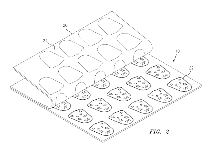
[0020] FIG. 2 is a top, side perceptive view of the sacrificial carrier
substrate shown in
FIG. 1 with bonded waste areas or regions partially separated from the
transfer sheet;
4
CA 02996986 2018-02-27
WO 2017/035437 PCT/US2016/048888
[00211 FIG. 3 is a schematic sectional elevation of one exemplary
embodiment for
transferring the sharply defined single elements from the transfer sheet to an
object to be
protected such as a banknote; and
[00221 FIG. 4 is a schematic, top planar view of a converting machine
wherein a web of
high value documents is precisely brought into contact with hot stamping dies
and a web of
isolated patches.
DETAILED DESCRIPTION OF THE INVENTION
[00231 Other features and advantages of the invention will be apparent
to one of
ordinary skill from the following detailed description. Unless otherwise
defined, all technical and
scientific terms used herein have the same meaning as commonly understood by
one of ordinary
skill in the art to which this invention belongs. All publications, patent
applications, patents and
other references mentioned herein are incorporated by reference in their
entirety. In case of
conflict, the present specification, including definitions, will control. In
addition, the materials,
methods, and examples are illustrative only and not intended to be limiting.
[00241 One aspect of the invention provides a single transfer process.
This process
comprises (a) providing a carrier substrate; (b) applying a separation layer
to a surface of the
carrier substrate; (c) applying a film material or resin structure (e.g., a
micro-optic film material
assembly) to a surface of the separation layer (d) applying an adhesive layer
to a surface of the
applied film material or resin structure; (e) cutting a plurality of cuts or
cut marks into at least one
of the adhesive layer, the film material or resin structure, or the separation
layer to produce
isolated single elements for transfer and a background element or background
elements.
[00251 By this process, a pre-patch transfer die-cut sheet is produced
that comprises (1)
a carrier substrate; and (2) a pre-patch transfer assembly that is affixed
along a first side of the
carrier substrate and which itself comprises (a) at least one isolated element
for transfer which
comprises (i) a material layer disposed along a first side of the carrier
substrate and which in its
uncut state may not be susceptible to conventional die-stamping processes; and
(ii) an adhesive
layer affixed along a first side of the material layer and opposite the
carrier substrate; and (b) a
background or waste element/region that is adjacent to or surrounds the at
least one isolated
element for transfer that is itself affixed along the first side of the
carrier substrate and is
separated from the isolated element for transfer by one or more cut marks.
CA 02996986 2018-02-27
WO 2017/035437 PCT/US2016/048888
[00261 In an exemplary embodiment, the single transfer process further
comprises
transferring the isolated element for transfer to an object to be protected.
Here it should be
noted that the cutting step (e) can be done by various methods including but
not limited to the
use of a die-cutting device having particular design shapes or configurations.
The cutting step
produces a separation between the isolated elements and the background element
or
background element(s). Here, it should be understood that the isolated element
for transfer and
the background element(s) may be of the same or of different layered
construction. However, in
preferred embodiments, the background element(s) and the isolated element for
transfer are of
identical construction. The die cutting step can be applied to cut through any
number of the layers
but must leave uncut at least one layer, preferably the layer at the furthest
distance from the
adhesive layer. In a particular embodiment, the cutting step (e) comprises
applying the die to cut
through the adhesive layer, the tear resistant material layer, and any other
layer(s) between the
material layer and the carrier substrate. This cutting step produces a pre-
patch transfer die-cut
sheet wherein the cut marks of a desired depth separates the isolated elements
for transfer from
the background element(s) for removal.
[0027] In the application step (g) a die stamp having a desired design
with desired
pressure points is placed in alignment with the isolated elements for transfer
and applied to an
opposing second side of the carrier substrate while the pre-patch transfer die-
cut sheet is affixed,
via the adhesive layer, to an object to be protected. The die stamp through
applied pressure
and/or heat applied by the pressure points in the die-stamp's design, applies
a force and/or heat
to the isolated elements for transfer and a lesser or non-existent force
and/or heat to the
background element(s) for removal. Due to the cut marks, the isolated elements
for transfer shall
be transferred and affixed to the object to be protected and the background
element(s) and the
carrier substrate can be cleanly and rapidly removed from object leaving
behind the isolated
element(s) for transfer on the object.
[00281 In the dual transfer process, a step (f) is interjected between
steps (e) and (g),
whereby a sacrificial carrier layer is applied to a first side of the adhesive
layer in the pre-patch
transfer die-cut sheet, opposite the carrier substrate. In one embodiment of
this aspect, the die-
stamp is applied to a first side of the sacrificial carrier layer opposite the
carrier substrate and the
adhesive layers. Here however, the design on the die-stamp is such that
pressure points are
6
CA 02996986 2018-02-27
WO 2017/035437 PCT/US2016/048888
aligned with the background element(s) for removal Due to the cut marks, the
background
element(s) for removal can be easily and rapidly removed from the carrier
substrate onto the
sacrificial carrier substrate, leaving behind the isolated element(s) for
transfer on the carrier
substrate. This forms the pre-patch transfer sheet. In a second transfer step,
the pre-patch
transfer sheet is applied to an object to be protected by placing the adhesive
layer of the at least
one isolated element for transfer against the object. Advantageously, while it
is possible to use a
die-stamp with a design having pressure points corresponding to the placement
of the at least
one isolated element for transfer; this is not required. By this process, it
is possible to use a die
stamp of various designs with or without pressure points corresponding to the
placement of the
at least one isolated dement for transfer. This significantly increases the
speed at which the
isolated element for transfer can be transferred to the object to be
protected. The sacrificial
carrier substrate may be composed of various materials which may be different
or identical to the
carrier substrate. For example, and as described below, the material may
comprise polyethylene
terephthalate (PET).
[0029] In one embodiment, the pre-patch transfer die-cut sheet or the
pre-patch transfer
sheet may have any combination of alignment between the separation layer, the
tear resistant
material, and the adhesive layer. For example, the separation layer may cover
the entire carrier
substrate or it cover only the areas corresponding to the isolated element(s)
for transfer, or some
discontinuous area slightly larger (e.g., 0.1mm to 0.4mm) or slightly smaller
(e.g., 0.2mm) than
the isolated element(s) for transfer. Similarly, it is also contemplated that
additional layers may
be incorporated into the sheets that are similarly registered or unregistered
to the isolated
element(s) for transfer; this includes the adhesive layer described herein or
additional adhesive
layers. For example, in one embodiment the adhesive layer described herein may
cover the
isolated tear resistant material or it may cover the background element(s) as
well Where it covers
the background element(s) as well, one of ordinary skill in the art will
understand that the
thickness of such an adhesive layer must be selected to avoid interfering with
the dean separation
of the background element(s) from the isolated element(s) for transfer during
the application
process to the sacrificial carrier substrate or to the object to be protected.
[0030] In one embodiment, the object to be protected is an object that
may be
counterfeited or misidentified. Persons of ordinary skill in the art would be
able to identify such
objects. For example, such object may include security paper used to form
security documents
7
CA 02996986 2018-02-27
WO 2017/035437 PCT/US2016/048888
such as high value documents including but not limited to currency banknotes,
checks, promissory
notes and the like. Alternatively, the security documents may be government
issued documents
including but not limited to documents such as passports, ID cards, stamps and
the like. It is also
contemplated herein that the isolated elements for transfer may be applied to
commercial
products. These isolated elements are suitable and are contemplated to provide
security and/or
aesthetic effects to the products or objects to which they are attached.
[0031] The cutting step (e) allows the use of a foil stamping process in
the application of
material (e.g., micro-optic film material assembly, or the like) to an object
with high resolution.
That is to say that the isolated element(s) for transfer, including but not
limited to patches of
micro-optic film material assembly, when applied to the object to be
protected, will have clean
sharp lines. In one embodiment, the edges of the isolated elements for
transfer are straight. In
another embodiment, the lines have very few ridges and are therefore sharply
defined. This
improves the printability of the object, where for example it is a banknote,
because there is less
fraying of print indicia and better (i.e., cleaner lines) resolution of the
printed indicia. This also
improves the aesthetic effect of the object.
[0032] In an exemplary embodiment of the single transfer process, the
plurality of single
elements are elongate patches or stripes that extend along the length of a
continuous sheet of
security paper or security documents such as banknotes. Step (e) is performed
using a precision
die cutting operation and step (g) is performed using a die stamping
operation.
[0033] In one such embodiment (i.e., type 1, registered stripe), a
series of closely spaced
die cut lines (e.g., 5 cuts at 2 millimeter (mm) increments) are placed in the
elongate patches or
stripes at those locations where the lead edge and optionally also the rear
edge of the stamping
die will contact the elongate patches during transfer from the transfer sheet
to the continuous
sheet of security documents. The series of closely spaced die cut lines allows
for registration
uncertainty. As noted above, no waste removal step (i.e., step (f)) is
required using this technique.
[0034] In another such embodiment (i.e., type 2, random registration),
which may be
combined with the previous embodiment, the elongate patches are cut to assure
that each
security document (e.g., banknote) has an elongate patch or stripe starting at
least as high as the
first document or note and to minimize any portion of any patch or stripe
spanning more than
one note (i.e., tail length overshoot). For example, while it is not known
where the starting and
ending edges of each stripe will fall, one can calculate the distance from the
stripe start to the top
8
CA 02996986 2018-02-27
WO 2017/035437 PCT/US2016/048888
of the first document or note, for example, 20 mm. The elongate patches are
then cut at regular
intervals along their length (e.g., every 20 mm or less). These cuts may
further frustrate potential
harvesting. Moreover, the shape of the cut may be complex to add to the design
if visible in the
final document or note.
[0035] In an exemplary embodiment of the dual transfer process, step (e)
is performed
using a precision die cutting operation, and step (f) is performed using a
patterned die stamping
operation. During step (f), the carrier substrate and the sacrificial carrier
substrate are brought
together, subjected to the patterned die stamping operation (including heat
and pressure), and
after each substrate or web has had sufficient time to cool, the two
substrates or webs are peeled
from each other and the background or waste regions surrounding the single
elements (e.g.,
patches) stay with the sacrificial carrier web and the original carrier web is
left with the desired
patches. The adhesive is now only on an upper surface of each patch, which may
then be
transferred to, for example, a security document.
[0036] In an exemplary embodiment of the inventive single or dual
transfer process, one
or more additional cut lines are incorporated in the cutting die design, which
do not have a
corresponding design element on the stamping or transfer die. The additional
cut line(s) within
each single element (e.g., patches, long strips) constitutes a very desirable
secure tearing feature
that provides additional tamper resistance, discouraging even careful removal.
These cut lines
can also function to add to the visual design and thus the security value of
the single elements.
[0037] In another exemplary embodiment, step (g), which is also
performed using a die
stamping operation, involves the transfer of the single elements in register
to one or more designs
on, for example, a security document.
[0038] The present invention further provides a process for forming a
transfer sheet
made up of a plurality of relatively non-tearable or tear resistant, single
elements on a carrier
substrate, each single element having a sharp definition, wherein the process
comprises process
steps (a)-(e), as described above.
[0039] The terms "sharply defined" and "sharp definition", as used
herein, are intended
to mean single elements having clearly defined, distinct shapes and details
including sharp
corners, small radius (e.g., 0.2 millimeter (mm)) holes, islands, patterned or
serrated edges,
and/or text elements, which are prepared using a precision die cutting
operation.
9
CA 02996986 2018-02-27
WO 2017/035437 PCT/US2016/048888
[0040) The present invention also provides such a transfer sheet, which
in an exemplary
embodiment comprises a plurality of micro-optic single elements for transfer
to objects to be
protected, wherein each micro-optic single element forms one or more
synthetically magnified
images.
[004111 In one such embodiment, the transfer sheet is a pre-patch
transfer, die-cut sheet
(i.e., a sheet before areas surrounding the cut single elements are
transferred from the carrier
substrate to a sacrificial carrier substrate and before the cut single
elements are transferred to an
object(s) to be protected). The inventive sheet comprises:
a carrier substrate;
a pre-patch transfer assembly that is affixed along a first side of the
carrier substrate that
comprises:
at least one isolated element for transfer having (i) a micro-optic film
material
assembly that produces a synthetic image and (ii) an adhesive layer affixed
along a first
side of the micro-optic film material assembly opposite the carrier substrate;
and
a background or waste element adjacent to or surrounding the at least one
isolated element for transfer that is affixed along the first side of the
carrier substrate and
that is separated from the at least one isolated element for transfer by one
or more cut
marks.
[0042) In another such embodiment, the transfer sheet is a pre-patch
transfer sheet (i.e.,
a sheet after areas surrounding the cut single elements are transferred from
the carrier substrate
to a sacrificial carrier substrate but before the cut single elements are
transferred to an object(s)
to be protected). The inventive sheet comprises:
a carrier substrate; and
a pre-patch transfer assembly that is affixed along a first side of the
carrier substrate and
that comprises:
at least one isolated element for transfer having (i) a micro-optic film
material
assembly that produces a synthetic image and (ii) an adhesive layer affixed
along a first
side of the micro-optic film material assembly opposite the carrier substrate;
and
a background area from which material has been removed that is adjacent to or
surrounds the at least one isolated element for transfer.
CA 02996986 2018-02-27
WO 2017/035437 PCT/US2016/048888
[0043) A process for applying one or more single elements to an object
to be protected
is also provided, the process comprising using the transfer sheet described
above to transfer the
single element(s) onto a surface of the object.
[00441 Further provided is an object to be protected, the object
displaying one or more
relatively non-tearable or tear resistant, single elements having sharp
definition applied to a
surface thereof. In an exemplary embodiment, the one or more single elements
are (a) micro-
optic single elements, (b) prepared and applied using the single or dual
transfer process described
above, and/or (c) applied using the transfer sheet described above.
[0045] Referring now to FIG. 1, there is shown an exemplary embodiment
of the transfer
sheet 10 during the dual transfer process of the present invention with cut
marks 11 before the
transfer sheet and a sacrificial carrier substrate 20 are brought together and
before areas
surrounding cut single elements on the transfer sheet (i.e., waste regions)
are transferred to the
sacrificial carrier substrate. The transfer sheet 10 comprises four (4) layers
including a carrier
substrate 12. The carrier substrate 12 has a thickness ranging from about 10
to about 30 microns
and may be formed of one of a number of different types of material including
a polymeric film
prepared using, for example, cellulose tri-acetate, polyester, polyethylene,
PET, polypropylene
(e.g., biaxially oriented polypropylene), polystyrene, polyvinyl carbonate,
polyvinylidene chloride,
and combinations thereof. A separation layer 14 made from a wax or lower
adhesion or tack
material (e.g., polyethylene, silicone) having a thickness of less than or
equal to about 1 micron
(preferably ranging from about 1 molecular layer to about 1 micron is applied
to the carrier
substrate 12. When the separation layer 14 is used with a micro-optic film
material having an
exposed lens layer, the separation layer may have a relief structure on one
surface that mates or
conforms to the exposed lens layer of the micro-optic film material.
[0046) A relatively non-tearable or tear resistant film material or
resin structure 16
having a thickness ranging from about 5 to about 30 microns is applied to the
separation layer 14.
[0047) In one preferred embodiment, the material or structure 16 is a
micro-optic film
material. As noted above, such materials form or project one or more
synthetically magnified
optical images, and generally comprise: at least one arrangement of image
icons, and at least one
arrangement of optionally embedded focusing elements positioned to form and
project one or
more synthetic images of at least a portion of the arrangement(s) of image
icons. These projected
images may show a number of different optical effects. Such structures are
described in U.S.
11
CA 02996986 2018-02-27
WO 2017/035437 PCT/US2016/048888
Patent No. 7,333,268 to Steenblik et al., U.S. Patent No. 7,468,842 to
Steenblik et al., U.S. Patent
No. 7,738,175 to Steenblik et al., U.S. Patent Application Publication No.
2014/0376091 Al to
Jordan etal.; International Patent Publication Number WO 2005/106601 A2 to
Commander etal.,
and International Patent Publication Number WO 2007/076952 A2 to Kaule et al.
[0048] The term "micro-optic film material" or "micro-optic film
material assembly", as
used herein, is intended to mean a system for projecting one or more synthetic
images that
comprises at least one arrangement of optionally embedded focusing elements
(e.g., micro-
lenses) and at least one arrangement of image icons (e.g., image icons (i) in
the form of posts
formed from one or more pigmented materials, (ii) in the form of posts where
areas surrounding
the posts are coated and/or partially or completely filled with one or more
pigmented materials,
or (iii) in the form of voids or recesses which are coated and/or partially or
completely filled with
one or more pigmented materials), wherein the arrangement(s) of optionally
embedded focusing
elements are positioned to form and project one or more synthetic images of at
least a portion of
the arrangement(s) of image icons.
[0049] The terms "synthetically magnified image" or "synthetic image",
as used herein,
is intended to mean that the image is synthetized by the united performance of
a multiplicity of
individual focusing element/image icon systems. Each focusing element
magnifies a dot/very
small space of the image below the focusing element, the dots are then
combined and projected,
thus leading to a magnified image, which is a synthetic image.
[0050] An adhesive layer 18 having a thickness ranging from about 3 to
about 12 microns
is applied to a surface of the film material or resin structure 16. Suitable
adhesives are not limited
and include, but are not limited to, thermoplastic adhesive systems including
acrylics (e.g.,
poly(methyl methacrylate)) and polyurethanes, and thermally activated
adhesives (i.e., hot melt
or heat seal adhesives).
[0051] The sacrificial carrier substrate 20 has a thickness ranging from
about 8 to about
40 microns and may be formed of the same material(s) noted above for carrier
substrate 12. The
sacrificial carrier substrate 20 may also be formed of paper materials or
combinations of paper,
film(s) and coating(s) that satisfactorily bond to the adhesive layer 18.
Optionally, the sacrificial
carrier substrate 20 can be coated with an adhesive that is similar or
complementary to the
adhesive used to form adhesive layer 18.
12
CA 02996986 2018-02-27
WO 2017/035437 PCT/US2016/048888
[00521 Prior to bringing the sacrificial carrier substrate 20 into
contact with the adhesive
layer 18, a precision die cutting operation is used to cut a plurality of
single elements (e.g.,
patches, long strips) 22 in the film material or resin structure 16 to a depth
that does not reach
(or substantially penetrate) the carrier substrate 12, thereby forming the
inventive transfer sheet
10. Optionally, the precision die cutting operation may be done in
registration to design elements
(e.g., a patch or other region of small or large size) on the film material or
resin structure 16. The
precision die cutting operation is performed on or slightly offset from the
intended pattern of
single elements (i.e., the planned transfer pattern). The amount and direction
of offset can be
adjusted to optimize the sought after result of cleanly transferring the
desired pattern. The
accuracy of die cutting to transfer pattern is maintained at a tolerance of
less than about 1
millimeter (mm), preferably less than about 0.2 mm.
[00531 Once the sacrificial carrier substrate 20 is brought into contact
with the precision
cut sheet, a patterned and heated stamping die is used to precisely press and
heat areas
surrounding the cut single elements (i.e., background or waste areas) causing
the adhesive to
adhere to the sacrificial substrate. As best shown in FIG. 2, the two webs are
then separated,
thereby transferring background or waste areas 24 surrounding the cut single
elements 22 from
the precision cut sheet to the sacrificial carrier substrate 20, leaving cut,
isolated single elements
22 behind. The patterned die stamping operation can be performed using
precision rotary or
intermittent motion flat-bed stamping. As will be appreciated by those skilled
in the art, the
operating temperature(s) used during the patterned die stamping operation is
adjusted based on,
for example, the processing speed, and factors including thermal transfer
properties and adhesive
bonding conditions. The speed is adjusted based on the temperature(s), dwell
time(s), as well as
adhesive and thermal transfer properties.
[00541 A rotary machine was used to execute the inventive dual transfer
process using a
web measuring 200 mm in width with a repeat period of 70 centimeters (cm).
Speeds of greater
than 30 meters per minute were demonstrated. Registration between the die and
stamping
operations achieved the required tolerance to successfully remove the waste
areas or regions in
precise alignment. A resin coated paper was used for the sacrificial carrier
substrate. The rotary
machine was capable of synchronizing to pre-defined design elements on the
starting web. An
eyespot was used to synchronize the web to the rotary machine.
13
CA 02996986 2018-02-27
WO 2017/035437 PCT/US2016/048888
[0055) Once prepared, the inventive transfer sheet 10 with sharply
defined single
elements 22 (e.g., a web of isolated patches or long strips) may be handled
like a traditional
transfer foil, that is, the material can be wound and unwound from a roll. The
web of patches or
long strips, which are matched with adhesive one for one, may be easily used
by a downstream
operation to transfer clean and consistent patches or strips to, for example,
high value
documents. The long strips may span the entire length of the high value
document. As noted
above, the complexity of the patches or long strips may be increased to
provide additional security
and tamper resistance. For example, holes/islands may be further included in
the transferred
patch or strip.
[00561 In a subsequent step or downstream operation, which is best shown
in FIG. 3, a
heated or hot stamping die 26 that is optionally sized larger (e.g., 1 to 5 mm
larger) than the
sharply defined single elements 22 is used to transfer the single elements
from the transfer sheet
to objects to be protected (e.g., banknotes) 28. By way of example, a high
value document
converting machine such as an OPTI-NOTAT" or similar machine may be used to
transfer the single
elements to a required position over a banknote by detection of suitable
register marks to locate
the single element directly under the hot stamping die 26 carried by the
converting machine. This
causes the adhesive to be bonded to the banknote to secure the single element
in the required
position.
[0057) In an exemplary embodiment in which the transfer sheet 10 is a
web of isolated
patches, an eyespot is incorporated on the web, which is used by an OPTI-
NOTAT" converting
machine to synchronize the web of isolated patches to one or more hot stamping
dies of the
converting machine. The web of isolated patches is brought into contact with
the hot stamping
die(s), which is larger than the isolated patches. The size of the hot
stamping die(s) is only limited
by the need to avoid contacting any surrounding patches. A web of high value
documents is then
precisely brought into contact with the hot stamping die(s) and the web of
isolated patches, each
patch containing an adhesive layer facing the web of high value documents. A
series of rollers
press the web of high value documents against the web of isolated patches and
the hot stamping
die(s). The adhesive regions flow onto and into the high value documents.
After a cooling period,
the web of isolated patches is peeled from the web of high security documents
leaving the patches
behind on the documents. The empty web is optionally run through the
converting machine to
remove remaining patches or wound to a waste take-up reel. Operating
conditions such as heat
14
CA 02996986 2018-02-27
WO 2017/035437 PCT/US2016/048888
or temperature, pressure and speed can be adjusted to optimize the transfer of
the patches to
the documents.
[0058] It is not unusual for such a machine to have nested regions on
the web of isolated
patches or roll of patterned film. The amount of overlap is a function of the
registration accuracy
of the patterned web and converting machine. In one such embodiment, as shown
in FIG. 4, the
height of transferred patches or regions A, B is significantly less than the
total height of each
banknote 28a, 28b, 28c, 28d. In this embodiment, two or more groups of patches
or regions can
be transferred on each pass of the web through the machine. In the case of two
passes, odd
patches or regions (i.e., regions A) might be transferred on a first transfer
operation 30 (Pass 1)
and the even patches or regions (i.e., regions B) might be transferred on a
second transfer
operation 32 (Pass 2). As will be readily appreciated by those skilled in the
art, passing the same
web or material two or more times through a converting machine increases the
yield of the
material.
[0059] As evident from the above description, the present invention
provides a wider
operating window for reliable conversion. An additional benefit is a much
higher web to
transferred single element utilization ratio. The transferred single elements
can be placed closer
to the edge of the carrier substrate and closer to each other. Area yield
improvements on the
order of 100% may be possible with the inventive process.
[0060] In addition, more complex object shapes may be formed using the
inventive
process resulting in better artistic integration and increased resistance to
simulation. Another
benefit is the ability to examine the film material or resin structure in the
background or waste
areas on the sacrificial carrier substrate. It is hard to monitor quality
aspects of the film material
or resin structure before transfer, so this added benefit presents a valuable
quality control
opportunity.
[0061] While various embodiments of the present invention have been
described above
it should be understood that they have been presented by way of example only,
and not
limitation. Thus, the breadth and scope of the present invention should not be
limited by any of
the exemplary embodiments.
SUBSTITUTE SHEET (RULE 26)