Note: Descriptions are shown in the official language in which they were submitted.
CA 02997184 2018-02-28
WO 2016/036420
PCT/US2015/024655
Patent Application for
TRANSFORMER
[0001] Related Applications
[0002] This application claims the benefit of U.S. provisional patent
application serial
number 62/046,782, filed September 05, 2014.
[0003] Field of the Invention
[0004] This invention relates to the field of transformers that convert an
incoming current to
an outgoing current, and especially where the incoming and outgoing currents
have different
voltages.
[0005] Background of the Invention
[0006] A typical electrical transformer utilizes inductive coupling between
two separate but
adjacent primary and secondary coils of wire. Current flowing through the wire
of one coil
(the primary coil) induces a current in the wire of the other coil (the
secondary coil).
[0007] One of the most common configurations of a transformer is the coaxial
transformer.
In a coaxial transformer, the primary and secondary coils usually are each a
tubular stack of
many loops with a cylindrical center passage, with the secondary coil
supported inside the
primary coil so that both coils have the same longitudinal axis. When AC
current is applied
to the primary coil, it creates a fluctuating magnetic field flowing through
the center, and
also around the outside of the primary coil. The fluctuating magnetic field
passes through
the center of the loops of the secondary coil, and this creates a
corresponding AC current in
the secondary coil.
[0008] The current in the secondary coil usually has a voltage that differs
from the input
voltage of the primary coil by a ratio that corresponds to the ratio of the
total area of all the
loops of the secondary coil to the total area of all the loops of the primary
coil.
[0009] An ideal transformer would convert 100 percent of the power applied to
the primary
-1-
CA 02997184 2018-02-28
WO 2016/036420
PCT/US2015/024655
coil to the current in the secondary coil, but in practice transformers are
much less efficient.
Conventional transformers lose power by the extension of the magnetic field of
the primary
coil away from the secondary coil, or by other areas of loss, e.g., by the
formation of
currents in the magnetic core of the transformer.
[0010] Some efforts have been made to reduce these losses, e.g., providing
shielding or
lamination surrounding the coils, but such arrangements continue to lose
power, and may
also create waste heat, with the result that transformers may require
complicated systems of
cooling elements to avoid overheating.
[0011] Summary of the Invention
[0012] It is accordingly an object of the present invention to provide a
transformer that
overcomes one or more of the drawbacks the prior art.
[0013] According to an aspect of the invention, an electrical transformer
comprises a
primary circuit extending between two ends. The primary circuit has at least
one of the ends
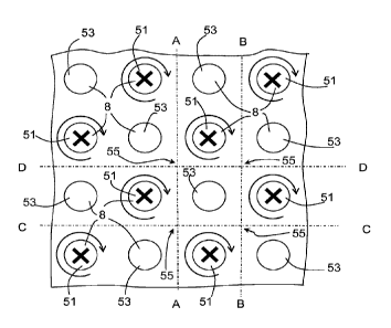
thereof connected with a power supply so that a first electrical current from
the power
source flows through the primary circuit. A secondary circuit is connected
with an electrical
load. The first and second circuits each have a respective plurality of wire
segments having
a length and being connected in series. The wire segments are supported so as
to extend in
pathways adjacent and parallel to each other over the length thereof so that,
when viewed in
cross section, the wire segments are arranged around a first point with the
wires of the
primary circuit alternating with the wires of the secondary circuit. The
current in the first
circuit causes formation of a second electrical current in the secondary
circuit that is
transmitted to the load.
[0014] Other objects and advantages of the invention will become apparent from
the
specification herein, and the scope of the invention will be set out in the
claims.
[0015] Brief Description of the Drawings
[0016] FIG. 1 is a schematic diagram of an embodiment of power transformer
according to
-2-
CA 02997184 2018-02-28
WO 2016/036420
PCT/US2015/024655
the invention.
[0017] FIG. 2 is a diagram of the cross section of a support structure of the
transformer of
FIG. 1.
[0018] FIG. 3 is a schematic diagram of the connections of the wiring of a
side of the
transformer of FIG. 1.
[0019] FIG. 4 is a schematic diagram of the wiring of the other side of the
transformer
shown in FIG. 3.
[0020] FIG. 5 is a detail diagram of the cross-section of the transformer of
FIG. 1 showing
the magnetic fields created around some of the wires of the primary circuit.
[0021] FIG. 6 is a diagram of a cross sectional view of an alternate
embodiment of the
invention, in which the wires of the primary and secondary circuits are in a
hexagonal cross-
sectional pattern.
[0022] FIG. 7 is a detail of the cross section diagram of the embodiment of
FIG. 6.
[0023] FIG. 8 is a schematic diagram of another alternate embodiment of the
invention,
wherein the circuits of the transformer are supported in three wire-supporting
structures.
[0024] FIG. 9 is a schematic diagram of still another alternate embodiment of
the invention,
wherein the circuits of the transformer are supported in four wire-supporting
structures.
[0025] FIG. 10 is a schematic diagram of still another alternate embodiment of
the
invention, wherein the circuits of the transformer are supported in a single
arcuate wire-
supporting structure.
[0026] FIG. 11 is a schematic diagram of a cross section of a wire support
structure of
another alternate embodiment, in which magnetically permeable elements are
provided in
the structure between the wires of the circuits.
[0027] FIG. 12 is a perspective detail view of the wire support structure of
FIG. 11.
[0028] FIG. 13 is a perspective view of a magnetically permeable element of
the
embodiment of FIG. 12.
[0029] FIG. 14 is a detail front view of stacked magnetically permeability
elements as
-3-
CA 02997184 2018-02-28
WO 2016/036420
PCT/US2015/024655
shown in FIG. 12.
[0030] FIG. 15 is a schematic of a cross-section of another embodiment of the
invention in
which magnetically permeable elements are present between the circuit wires.
[0031] FIG. 16 is a perspective view of a magnetically permeable element as
shown in FIG.
15.
[0032] FIG. 17 is a schematic diagram of a cross-section of another embodiment
of the
invention that allows for a 2:1 increase in voltage of current applied to the
transformer.
[0033] FIG. 18A is a schematic of a cross-section of another embodiment of the
invention
in which the primary and secondary circuits are formed of bundles of wires in
the support
structures in a rectangular matrix pattern.
[0034] FIG. 18B is a schematic of a cross-section of another embodiment of the
invention in
which the primary and secondary circuits are formed of bundles of wires in the
support
structures in a hexagonal close-packed pattern.
[0035] FIG. 19 is a schematic illustrating the wiring of a step-up transformer
according to
the invention.
[0036] FIG. 20 is a diagram of another embodiment of transformer according to
the
invention, where the wires are surrounded by a lattice-type structure of
material that
influences the interacting magnetic fields between the primary and secondary
circuits.
[0037] FIG. 21 is a perspective cutaway view of another alternate embodiment
of wire
support structure for a transformer according to the invention.
[0038] FIG. 22 shows the beginning of a wiring winding for making a
transformer
according to the invention.
[0039] FIG. 23 is a view of the winding of FIG. 21 with an additional loop
applied to the
circuit.
[0040] FIG. 24 is a view as in FIG. 23, wherein a number of additional
circuits have been
added to the underlying circuit shown in FIG. 23.
[0041] FIG. 25 is a view taken along line X-X of FIG. 24.
-4-
CA 02997184 2018-02-28
WO 2016/036420
PCT/US2015/024655
[0042] FIG. 26 is a view as in FIG. 25 with additional loops of wire applied
alongside the
first set of loops.
[0043] FIG. 27 is an exemplary detail cross section of a configuration of the
wires of FIG.
26.
[0044] FIG. 28 is a partial perspective view of an initial part of an
alternative embodiment
of transformer wiring winding for making a transformer according to the
invention.
[0045] FIG. 29 is a side view of the winding of FIG. 28.
[0046] FIG. 30 is a view as in FIG. 29, but with an additional outer layer of
winding
thereon.
[0047] FIG. 31 is a partially cutaway cross sectional view through a vertical
middle plane of
the winding of FIGS. 28 to 31 with four layers of winding thereon.
[0048] FIG. 32 is a cross-sectional detail view of a cable having two wire
bundles therein
that may be used in the embodiment of FIGS 28 to 32.
[0049] FIG. 33 is a cross-sectional diagram of a transformer according to the
invention with
an additional extension of the secondary coil applied on top thereof.
[0050] Detailed Description
[0051] As has been mentioned, the transformers of the prior art are typically
made up of two
discrete sets of multiple loops arranged coaxially, often with one entire
circuit of loops
radially inside the other, with the magnetic field flux occurring essentially
in the center of
the loops. In contrast, the present invention generally makes use of the
exchange of
magnetic flux between adjacent generally parallel wires or bundles of wires
extending
through supportive structures that hold the wires in parallel configuration
with each other. In
the parallel arrangement, the wires or wire bundles of the wires being
supplied with power
(the primary circuit) are distributed rotatively-spaced around the lengthwise
axis of the
wires or wire bundles receiving the magnetic flux and generating the output
current (the
secondary circuit). The result is a more efficient magnetic-flux interaction
of the respective
-5-
CA 02997184 2018-02-28
WO 2016/036420
PCT/US2015/024655
wires or wire bundles.
[0052] The general arrangement of a transformer according to the invention is
illustrated in
the embodiment of FIG. 1. An electrical power transformer system generally
indicated at 9
connects an AC power source 11 to load 13. The AC power source may be any
power
source desired, such as, for example, standard American 120-volt 60-Hz AC
house current.
The load 13 may be any type of electrical load or device, e.g., a motor, a
lamp, or any sort of
electrical device or converter.
[0053] The power source 11 transmits a current in wire segment 14, which
carries the
electrical current to the transformer system generally indicated at 9, the
current returns to the
other pole of the power source 11 via wire segment 15. Between the input and
output wire
segments 14 and 15, the current is routed through a primary transformer
circuit formed of
wiring in wire support structures 1 and 2, and connecting wires generally
indicated at 3 and
5, as will be described below. Wire segments 16 and 17 connect load 13 with a
secondary
circuit also formed by the wiring in the support structures 1 and 2 and the
connecting wires
3 and 5. Electrical current is generated in the secondary circuit responsive
to passage of the
current through the primary circuit from the power source 11, and the
electrical current
generated in the secondary circuit is supplied to the load 13 via wire
segments 16 and 17.
[0054] Referring to FIG. 2, wire support structures 1 support the wires of the
primary and
secondary circuits to extend in parallel through the length of the support
structure, with the
wires being in the same relative positions over its length. The arrangement of
the wires in
the support structures is such that the current in the primary circuit
efficiently produces the
current in the secondary circuit, making optimal use of the magnetic fields
produced around
the wires of the primary circuit.
[0055] The body 7 of the support structure is shown generally in schematic
form. One of the
primary functions of the body 7 is to support the wires 8 in their same
relative positions to
each other over the length thereof.
[0056] In addition, in the transformer of the invention, it is preferable that
the inductance
between the primary and secondary circuits is enhanced by the use of magnetic
core
materials in the support structure body 7 between the wire segments of the
primary and
-6-
CA 02997184 2018-02-28
WO 2016/036420
PCT/US2015/024655
secondary coils. To achieve this, the body 7 may be formed of an electrically-
insulating
material of high magnetic permeability, such as high-density polyethylene
(HDPE), PVC, or
some other insulating plastic material mixed with some sort of iron-containing
or other
magnetic metal-containing particles, granules or powder, such that the plastic
structure has
magnetic qualities that intensify the magnetic fields and inductance between
the wires
passing through it. The body 7 may also be made of other materials, such as
non-conductive
terrific materials in a structure encasing the primary and secondary circuits,
as will be set
out herein, or the body 7 may be a structure formed of a large number of
mutually insulated
iron-containing elements forming a lattice structure around the wires, such as
any of the
matrix wire-supporting structures shown in FIGS. 11 to 16 or 20 to 21.
[0057] The pattern of the positions of the wires of the primary and secondary
circuits may
be one of several possible arrangements. The general principle of the
arrangement is that,
for at least some of the wires of the primary circuit in the support
structures 1, 2, e.g., in the
interior of the body 7, each wire has a number of wires of the secondary
circuit grouped
around it, rotatively distributed around an axis of the primary circuit wire.
Preferably, the
number of wires is three or more, and the distribution of the secondary
circuit wires is by
successive equal angular rotations, e.g., 90 degrees or 120 degrees.
[0058] FIG. 2 shows one possible cross-section of the organization of the
wires 8 in wire
support structure 1. The cross-sectional pattern is taken through the support
structure 1
perpendicularly to the wires 8. The cross section of support structure 2 is a
mirror-image of
support structure 1, in terms of the positions of the primary and secondary
wires. The cross-
sectional patterns are substantially constant over the length of the
structures 1 and 2.
[0059] The body 7 supports the wires in a square 6x6 matrix pattern in the
embodiment
shown. Wires of the primary circuit of the transformer system are indicated by
reference
characters "P" and the wires 8 of the secondary circuit are indicated by
reference characters
"S". The primary circuit wires P and the secondary circuit wires S alternate
with each other
in both the horizontal rows and the vertical columns of the cross-section
matrix. The wires 8
are each at least 0.10 inch from the adjacent wires 8 in the row or column.
[0060] Support structures 1 and 2 are physically the same, and the wires 8 are
identical, and
-7-
CA 02997184 2018-02-28
WO 2016/036420
PCT/US2015/024655
may be any conductor, insulated wire, twisted conductive wires, or a number of
independently insulated bundles of wires as will be described below. The
positions of the
primary and secondary circuit wires are a consequence of the specific
locations of the
connections of the connective wires 3 and 5 between the support structures 1
and 2, and the
placement of the connection of wires 14, 15, 16 and 17 to individual wires 8
in the support
structures.
[0061] FIG. 3 shows in the wiring pattern of the set of connecting wires 3
that extend
between the rear faces 19 of the support structures 1 and 2. The wires 8 are
shown as circles,
with darker circles indicating the wires 8 of the primary circuit, and light
circles the wires 8
of the secondary circuit.
[0062] The wires 3 are each insulated, and each connects a respective end of a
wire 8 in
support structure 1 with a respective end of a wire 8 in support structure 2.
The set of wires
3 comprises a set of six wires 3a, 3b, 3c, 3d, 3e and 3f for each row of wires
8 in the matrix
pattern of the structures 1 and 2. In each row, wire 3a electrically connects
the laterally
innermost wires 8 in structures 1 and 2. Wires 3b electrically connect the
next outward wires
8 in the row, as do wires 3c, 3d and 3e. The laterally outermost wires 8 are
electrically
connected to each other by wires 3f. Essentially, the connections are
laterally symmetrical
across the two matrices.
[0063] FIG. 4 is a schematic of the front ends of a pair of support structures
1 and 2, and
shows the wiring the set of connecting wires 5 of front faces 18 of the
support structures 1
and 2. These connections create a group of circuits in the transformer system
9 that
constitute the primary and secondary circuits. Eighteen loops are formed in
the primary
circuit, and another eighteen loops are formed in the secondary circuit. The
darker colored
circles correspond to the primary winding circuit, and the white circles
correspond to the
secondary circuit. The two winding circuits are not in electrical contact, but
a current in one
magnetically induces a current in the other. Both the primary and secondary
winding circuits
form loops around the center of the transformer 9.
[0064] Wires 5 are electrically insulated, and each wire 5 electrically
connects an end of a
respective wire 8 in structure 1 to an end of a respective wire 8 in structure
2. AC power line
-8-
CA 02997184 2018-02-28
WO 2016/036420
PCT/US2015/024655
15 is connected to the first wire in the bottom row of the matrix of wires in
front face 18 of
support structure 1. Load connecting wire 17 is connected with the second wire
8 in the
bottom row of the matrix of wires in structure 1. The other AC power line 14
is electrically
connected with the first wire 8 in the top row of the matrix of wires 8 in
support structure 2.
The other load connecting wire 16 is electrically connected with the second
wire 8 in that
row.
[0065] Current entering support structure 1 at wire 15 flows through the
bottom left wire 8
of structure 1 to opposite end 19 of structure 1. It there is connected by one
of wire set 3
with the distal end of the last wire in the bottom row of wires 8 in structure
2. The current
then flows through that wire 8 to its proximal end 21 in the front end 18 of
structure 2.
[0066] Lead line 17 electrically connects with the second wire 8 of the bottom
row of
structure 1. That wire 8 extends through to the distal end of the structure 1
where one wire
of connecting wire set 3 connects it with the next-to-last wire 8 in the
bottom row of wires
in structure 2, which extends through to a proximal end 23 thereof in the
front end 18 of
structure 2.
[0067] Wire end 21 is connected via end wire 5a to the third wire 25 of the
bottom row of
structure 1, i.e., with a shift two wires to the right. This forms the first
loop of the primary
circuit. Wire end 23 is connected by end wire 5b to the fourth wire end 27 in
the bottom row
of structure 1, forming the first loop of the secondary circuit.
[0068] Wire end 25 connects through structure 1, the respective end wire 3,
and then
through structure 2 with the front end 29 of the third from the last wire in
the bottom row of
wires 8 in structure 2. Wire end 27 connects through the structures 1 and 2
via the associated
end wire 3 to wire end 31. Wire ends 29 and 31 connect by end wires Sc and 5d
respectively
with wires 8 shifted two wires to the right, i.e., with wire ends 33 and 35
respectively,
completing the second loops of the primary and secondary circuits.
[0069] The third loops of the primary and secondary circuits are formed by the
wires 8 from
ends 33 and 35 extending through structure 1, relevant end wires 3 and back
through
proximal wire ends 37 and 39. The proximal ends 37 and 39 are connected via
front end
wires 5e and 5f to the first two wires 43 and 41, respectively, forming the
loops.
-9-
CA 02997184 2018-02-28
WO 2016/036420
PCT/US2015/024655
[0070] The wiring 3 and 5 at this point essentially repeats the pattern for
the bottom rows of
the structures 1 and 2 for all rows of wires, until the first two wires 45 and
47 of the top row
of structure 2, which, instead of being connected with wires 5e and 5f linking
up to the next
row, they connect with lines 14 and 16.
[0071] The wire segments of the primary and secondary circuits in the cross
sections of the
support structures alternate with each other in both horizontal and vertical
directions. In this
embodiment, eighteen loops are formed in the primary winding circuit, and
another eighteen
loops are formed in the secondary winding circuit. The two winding circuits
are not in
electrical contact, but a current in one magnetically induces a current in the
other.
[0072] FIG. 5 is a detailed diagram of a cross section of the wires in the
support structures 1
and 2. In the diagram, wires 51 are wires 8 of the primary circuit. The wires
53 are wires 8
of the secondary circuit. Lines AA and BB are the vertical centerlines between
the columns
of wires 8, and lines CC and DD are the horizontal centerlines between the
rows. These
vertical and horizontal centerlines intersect at intersection points 55. The
material of the
support structure between the wires 8 and along lines AA, BB, CC, and DD is
magnetically
permeable material. Arrows 57 around the wire segments 51 indicate the
orientation of the
magnetic field created in the primary circuit by current passing through it,
with the current
direction going into the page of the diagram.
[0073] Points 55 indicate central points or junctures that are each between
respective groups
of four wires 8, i.e., two primary circuit wires 51 and two secondary circuit
wires 53. The
wiring of the primary and secondary circuits is such that, proceeding
circularly around a
central point 55, the wires 8 alternate between wires 51 of the primary
circuit 51 and wires
53 of the secondary circuit 53, and each primary-circuit wire 51 in the
support structure is
surrounded by four secondary-circuit wires 53, except for the wires 51 on the
outer surface
of the support structure. The result is that there is an efficient
transmission of magnetic
energy between the primary and secondary circuits.
[0074] Generally, for the wires interior to the support structures 18, each
wire 8 of the
primary circuit extends through the support structure 18 with four wires of
the secondary
circuit extending adjacent and parallel to, rotatively displaced equally
around the primary
-10-
CA 02997184 2018-02-28
WO 2016/036420
PCT/US2015/024655
circuit wire at equal relative angles of 90 degrees. Similarly, internal wires
of the secondary
circuit extend through the support structure 18 with four wires of the primary
circuit
extending adjacent and parallel to it, rotatively displaced around the
secondary circuit wire
at equal relative rotative angles of 90 degrees. The wires of the circuits on
the outer surface
are adjacent to two or three wires of the other circuit, depending on whether
the wire is at
the corner of the matrix or on its edge, with the two or three opposite
circuit wires 8 being
rotatively staggered about the axis of the wire by equal angular displacements
of 90 degrees,
as well.
[0075] It will be understood that although the embodiment shown in FIGS. 1 to
5 has
support structures 1 and 2 that are each a 6x6 square matrix pattern, the
cross-sectional
matrix pattern of wires may be larger or smaller and still obtain advantages
of the invention.
The matrix also need not be square. Matrix patterns of wires may be virtually
any size of
rectangular or square matrix, e.g., 4x8, 100x100, 500x70, or a matrix with any
number of
rows and columns.
[0076] The functionality of the transformer derives from the support structure
holding
secondary wires surrounding each of the primary wires over the length of the
respective
structure so as to efficiently transfer energy between the primary circuit
wire and the
secondary circuit wires surrounding it. The specific sequential spiraling
order of the
connections of the primary and secondary circuit wires described above, i.e.,
the circuit
connections spiraling outward through the row, then up to the innermost
connection of the
circuit in the next higher row, and then outward through that row, is not
necessary to obtain
an advantageous operation of the transformer of the invention. For example,
alternatively,
the wires of each circuit may be connected with the wire ends of the support
structures in a
different progression pattern, or even by randomly connecting ends of wires in
one end of a
structure with the ends of the other wires in the other structure, provided
the alternating
pattern of primary and secondary circuit wires is maintained.
[0077] To put this more specifically, with reference to FIG. 2, in an
alternative wiring order,
the ends of each of the wires S of the secondary circuit may be connected with
a respective
randomly selected end of the secondary-circuit wires S in the other support
structure, and
the primary circuit wire ends P each connected with the ends of the primary
circuit wires P
-11-
CA 02997184 2018-02-28
WO 2016/036420
PCT/US2015/024655
of the other support structure, so that all the wires 8 indicated in dark
circles in FIG. 3 and 4
carry the current through the support structures 18, and the wires 8 indicated
by light-
colored circles are wired in series so as to produce a current from the
varying magnetic field
created by the primary circuit. The arrangement of alternating primary and
secondary
circuit wires remains the same as in the embodiment described above; only the
sequence of
their connection within the respective circuit would be varied.
[0078] FIG. 6 is a schematic diagram of the wire arrangement of an alternate
embodiment
of support structures 61 and 62 that may be used in support structures 1 and 2
of FIG. 1, and
the same reference numbers are used for equivalent parts.
[0079] Instead of a square-shaped matrix cross-section with rectilinear
coordinates, the
embodiment of FIG. 6 has a generally hexagonal shape. The support structures
61 and 62
are made up of insulated wires indicated as P or S, some of which are
identified by reference
characters 63 or 65. The wires are shown as members with a triangular cross-
section in FIG.
6, extending in parallel over the length of the structures 61 and 62. Each
wire is preferably a
core of conductor surrounded by a sheath of insulating magnetically-permeable
material.
The sheath need not be triangular, but the geometrical organization of the
substantially
parallel wires that are supported in the sheaths is important. The wires
marked "P" form the
primary circuit, and wires labeled "S" make up the secondary circuit.
[0080] The wiring of the front faces of the structures 61 and 62 is shown in
FIG. 6. As in
the previous embodiment, wires 14 and 15 connect to the power source 11, and
wires 16 and
17 connect to the load 13. Wire 15 is electrically connected to the first wire
63 of the
primary circuit P in the bottom row of wires in structure 61. Wire 17 is
connected with the
second wire 65 of the secondary circuit S in the bottom row of wires in
structure 61.
[0081] Wire 63 carries the current from line 15 to the opposing end of the
structure (not
shown) where the distal ends of all the wires in the structure are connected
similarly to the
end connection 3 of FIG. 3. The first wire 63 is connected by a wire to the
last wire 67 of
the bottom row of structure 62. The wire 65 connected with line 17 extends to
a distal end
wherein the end connecting structure 3 as in FIG. 1 connects with its minor
image position
in the cross-sectional wire pattern of structure 62, i.e., the next-to-last
wire 69 of the bottom
-12-
CA 02997184 2018-02-28
WO 2016/036420
PCT/US2015/024655
row of wires of structure 62.
[0082] To form the first loop of the primary circuit, front loop 71 connects
wire 67 to the
third wire 65 of the bottom row, returning back shifted two wires to the right
in the row.
Progressing horizontally across the row, the second wire from the end of the
bottom row of
structure 62 forms the first secondary circuit loop by electrical connection
via wire 73 to the
fourth wire in the bottom row of structure 61.
[0083] The primary and secondary circuits form subsequent loops by extending
through the
structure 61 then across to the mirror-image position wire in structure 62,
and then by front
loop connection wires 75 to wires shifted over two wires to the right in the
row. Finally for
the bottom row, the leftmost two wires 76 and 77 of the bottom row of
structure 62 connect
via row-shifting connecting wires 78 to the first two wires 79, 80 of the next-
to-bottom row
of structure 61.
[0084] This pattern is repeated for all the rows, i.e., mirror- image
connections of the distal
ends and shift right two wires for all connections in the front row, except
the leftmost two
wires of the rows of structure 62, which connect with the leftmost wires of
the next row up
in structure 61. That pattern continues up to the leftmost two wires of the
top row of
structure 62, which connect to the lines 14 and 16 to the AC power and the
load.
[0085] It will be understood that the wires P and S are illustrated
schematically in FIG. 6 as
triangles, but they may take a variety of forms, e.g., a central circular
cross section wire
embedded in a triangular shaped insulation-material body, or a typical
circular cross section
braided wire surrounded by a generally tubular sleeve of insulation, or almost
any other
configuration of conductor known in the art. The primary concern is that the
conductor
portion of the wires P and S should be supported over the length of the
carrier in the central
position in the triangular volumes shown in FIG. 6 and labeled P or S. Also,
they may be a
bundle of mutually insulated wires extending together in the space in the
bodies 18 or 19.
[0086] FIG. 7 shows a more detailed view of a cross-section of the structures
61 and 62.
Throughout the structure, wires P belonging to the primary circuit and wires S
belonging to
the secondary circuit are grouped so that three wires P and three wires S
surround each
central point Q in the structure. The wires P and S are substantially
equidistant from the
-13-
CA 02997184 2018-02-28
WO 2016/036420
PCT/US2015/024655
center points Q, and they alternate circularly around central points Q with an
angular
spacing of approximately 60 degrees between adjacent wires.
[0087] Each of the wires P or S forms part of three groups around three
different central
points Q, except for the wires P and S that are on the outer surface of the
carrier 61. As a
corollary, almost all of the wires P, i.e., those that are interior to the
carrier, are surrounded
by three parallel wires S, rotatively spaced at 120 degrees from each other
about the central
axis of the wire P. When current flows through the wires P, which in FIG. 7 is
indicated as
flowing in the direction into the surface of the diagram, the resulting
magnetic field has a
primary effect on the three surrounding parallel wires S, inducing a reactive
current therein.
Expressed somewhat differently, each wire S is acted upon primarily by the
magnetic fields
of three surrounding wires P that are rotatively staggered at equal angles
about wire S, i.e.,
at 120 degrees relative to each other.
[0088] Expressed somewhat differently, each wire P in the interior of the wire
support
structures of FIGS. 6 and 7 has three wires nearest adjacent it by which it is
surrounded, and
these wires are three secondary circuit wires S spaced rotatively at 120
degrees relative to
each other. The wires P on the outer surface of the wire support structures 61
and 62 have
only two immediately neighboring wires, but they are also wires S of the
secondary circuit
as well.
[0089] In addition to the progressive pattern of circuit connections described
above, it is
also possible to derive a benefit of the invention where the ends of the S
wires on the
support structures are connected in a different order or pattern, or even a
random pattern,
wherein each end of a wire S in support structure 18 connects with a
respective end of a
wire S in support structure 19. The main consideration is that each wire P in
the interior of
the support structure is surrounded by three immediate neighboring wires S of
the secondary
circuit.
[0090] FIG. 8 shows a schematic of an alternate embodiment having three
support
structures 81 similar to the 6x6 square matrix support structures 1 and 2
shown in FIG. 1.
Alternatively, structures such as shown in FIG. 6 may be employed. The primary
circuit
connects to a power source via leads or wire segments 84 and 88. The secondary
winding
-14-
CA 02997184 2018-02-28
WO 2016/036420
PCT/US2015/024655
circuit connects to a load via wire segments 86 and 90. Support structures 81
hold the wires
in parallel in a cross-sectional 6x6 matrix pattern (or in a square or
rectangular matrix or
hexagonal packing pattern of any number of wires), and electrically insulate
the wires from
each other, so that the primary circuit is electrically insulated from the
secondary circuit.
Connector arrangements 83 of wire segments connect the wires of the support
structures 81,
and are essentially the same as the wiring shown in FIG. 3, i.e., with a one-
to-one mapping
of the ends of wires to the same wire location in the next structure 81.
Connector
arrangement 87 of wires connect the wires of the front ends 82 of support
structures 81, with
a shift two wires to the right at each iteration so as to form the circuits.
The wiring pattern of
connection arrangement 87 is preferably the same as that shown in FIG. 4, but
may be any
pattern that connects all of the ends of the circuits so that the circuit
wires extend through
the carriers 81 in the alternating pattern shown in e.g., FIG 2. A central
space 85 is defined
by support structures 81 and is characterized by the absence of a central
core, in contrast
with conventional coaxial transformers.
[0091] FIG. 9 shows a schematic of another embodiment of the invention having
four
support structures 91 that are 6x6 matrix or other matrix or hexagonal pattern
structures
similar to those of FIG. 1. The primary circuit connects to a power source via
wire leads or
segments 94 and 98. The secondary circuit connects to a load via wire leads or
segments 96
and 100. Support structures 91 hold the wires in parallel a cross-sectional
pattern and
electrically insulate the wires from each other, and in particular the primary
circuit is
electrically insulated from the secondary circuit. One-to-one mapped wire
connection
arrangements 93 of wire segments with a pattern as shown in FIG. 3 connect the
wires of the
support structures 91. Connection arrangement 99 of wire segments connects the
wire ends
in front faces 95 of support structures 91, mapping the connections two wires
shifted to the
right for each iteration, with a connection pattern as described and shown in
the structure of
FIG. 4. A central space 97 is defined between structures 91, and it also has
no central core,
in contrast with conventional coaxial transformers.
[0092] FIG. 10 shows a schematic view of another alternate embodiment of the
invention
having only a single support structure 101. The primary circuit connects to a
power source
via leads or wire segments 104 and 108. The secondary circuit connects to a
load via wire
-15-
CA 02997184 2018-02-28
WO 2016/036420
PCT/US2015/024655
segments 106 and 110. Support structure 101 holds the wires in a cross-
sectional pattern,
e.g., a 6x6 matrix, constant over the entire length of the structure 101, with
the wires
electrically insulated from each other and extending through side-by-side
passages in the
structure 101. In particular, the primary circuit is electrically insulated
from the secondary
circuit and held at a constant spacing therefrom. A connection arrangement 103
of wires
connects the wires of the two ends 102 of the support structure. The
arrangement is similar
to that shown in FIG. 4, with wires in one end 102 being connected to wires in
the other end
102 shifted over by two wires, or in the next row upward, although other
patterns that
maintain the alternating primary and secondary circuit wire pattern may also
be employed.
The structure 101 defines therein a central space 105. Central space 105 is
empty, and lacks
a central core, which is in contrast with conventional coaxial transformers
that usually have
an iron or other metallic core.
[0093] FIG. 11 is a cross-section of an alternate embodiment of wire support
structure,
which may be used in place of the support structures of any of the previous
embodiments.
The structures between the wires modify the magnetic fields produced by the
primary
circuit. Wires connected so as be the primary circuit are indicated
schematically at 111 and
wires connected so as be the secondary circuit are indicated schematically at
113. The wires
111 and 113 may be single insulated wires, twisted wires in insulation, or
bundles of
mutually insulated parallel wires may be used.
[0094] The wires 111 and 113 extend through passages lined by a surrounding
sheath 117
that preferably also holds the wires in place. Wires 111 and 113 are arranged
in an
alternating pattern, and here form a six by six (6x6) matrix, but other sizes
of matrix can be
used. The alternating of wires 111 and 113 results in each primary-circuit
wire 111 having
four secondary-circuit wires 113 arranged around it extending alongside in a
constant cross
section over the length of the wires 111 and 113 above and below in its
column, and left and
right of it in its row. The wires on the outer surface of the matrix
arrangement, i.e., adjacent
to sheath 117 are an exception, and have fewer wires around them.
[0095] Wires 111 and 113 extend through a lattice structure formed by elements
of high
magnetic permeability 125 and 127 surrounding the wire segments. The wire
segments are
insulated from each other and from the elements 125 and 127. Elements 125 and
127 are
-16-
CA 02997184 2018-02-28
WO 2016/036420
PCT/US2015/024655
plate-like and planar, with the flat faces of the elements being
perpendicular, i.e., normal, to
the direction of extension of the wires, and the elements 125 and 127 are
preferably
supported in stacks, with the stacks extending over the entire length of the
wires 111 and
113.
[0096] The elements are notched to allow room for cooling sections 139 to run
along the
length of the wires 111 and 113. The cooling sections 139 may contain air, or
another
material, including solids and fluids, and a thermal cooling system may be
connected to
move the fluids. The wires 111 and 113 are arranged around cooling elements
139 such that
each cooling section 139 is a junction around which the wires 111 and 113
alternate.
[0097] FIG. 12 shows a partially cut away perspective detail view of a support
structure as
shown in FIG. 11. Wire segments schematically indicated at 131 are in the
primary circuit
and wire segments schematically indicated at 133 are in the secondary circuit,
and the
primary and secondary wires are arranged in an alternating pattern as in FIG.
11. In
addition, elements of high magnetic permeability 135 and 137 surround the wire
segments.
The elements are notched and surround cooling sections 139. The wires of the
primary or
secondary circuits are surrounded by a lattice of the elements 135 or 137 over
the length of
the wires. The elements are plates, and a single element only covers a small
portion of the
length of a wire, so they are stacked over the length of the support
structure. The elements
are insulated from each other, and by individual lamination for insulation, or
the insulation
may be air or another insulating material. Particularly preferred as an
insulator is
transformer oil. The wire segments themselves have insulation 134 around the
passages
through which they extend. Insulation 134 insulates the wire segments from
each other and
from the elements 135 and 137.
[0098] FIG. 13 is a perspective drawing of an element of high magnetic
permeability 135.
As mentioned above, the element 135 is preferably completely made of a
magnetically
permeable material, e.g. a ferritic material. The element 135 has a narrowed
central portion
141, and forked prongs 143, 145, 147 and 149. The prongs 143, 145, 147 and 149
are set at
approximately 45 angles from the central portion 141, and each terminates in
a
perpendicular face at 45 to the central portion 141.
-17-
CA 02997184 2018-02-28
WO 2016/036420
PCT/US2015/024655
[0099] The AC current passing through the core can give rise to a momentary
magnetic
north pole and a magnetic south pole, e.g., North at prongs 143 and 145 and
South at prongs
147 and 149, and then these magnetic poles will be immediately reversed when
the AC
current changes to the opposite direction.
[00100] Each element 135 has four indentions or recesses 140, 142, 146, and
148.
Elements 135 and indentations 146 and 148 are sized such that the elements 135
fit between
conductors, e.g., conducting wires 131 and 133 as in FIG. 12. The indentations
140 and 142
are sized to provide the cooling sections 139, which may be used as an
electrical insulator
and/or for thermal cooling.
[00101] FIG. 14 is a side view of a stack of laminated elements 135 as in FIG.
13. The
core's height is small compared to the length of a wire of a circuit. The
elements 135 are
preferably insulated from adjacent elements 135 above and below them, by,
e.g., lamination,
transformer oil, or some other relatively thin insulator. This reduces the
formation of stray
currents, which lead to reduced efficiency and unwanted heat buildup.
[00102] FIG. 15 is a cross-section of a support structure. Wire segments
belonging to the
primary circuit 151 and wire segments belonging to the secondary circuit 153
are arranged
in an alternating pattern. Cores of high magnetic permeability 157 surround
the wire
segments of the primary circuit. The wire segments are insulated from each
other and from
the cores by insulation 156. Cooling element 159 is found between cores and
may be air or
other thermal conductor.
[00103] FIG. 16 is a perspective drawing of a single general U-shaped element
of
conductive or ferromagnetic material 157. The element 157 has central section
161, and
prongs 163 and 164. The element also has indentation 165, which is sized to
fit around a
conducting wire, e.g. wire 151. The prongs 163 and 164 are set at an
approximately 45
angle from the central section 161 and provide faces 167 at 45 . During the
application of
AC power to the transformer, the elements 157 may be magnetized by the AC
current, such
that, momentarily, prong 163 has one magnetic pole and prong 164 has the other
magnetic
pole, and that magnetic polarity is reversed when the AC current reverses its
polarity.
[00104] Analogous types of metallic structures may be employed between the
wires of the
-18-
CA 02997184 2018-02-28
WO 2016/036420
PCT/US2015/024655
hexagonal pattern of FIG. 6, allowing for lengthwise cooling passages.
[00105] The foregoing embodiments have primary and secondary circuits that are
of
effectively the same length, which results in the voltage of the current of
the secondary
circuit being similar to that of the current in the primary circuit.
Transformers of that sort
have some utility, e.g., to smooth the voltage of an incoming current that
fluctuates
markedly. However, transformers normally are employed to change the voltage of
the
incoming current to a higher or lower voltage.
[00106] That is accomplished in the present invention by increasing the length
of the
wiring of the primary and/or secondary circuits. The length of a circuit is
accomplished by
increasing the number of wires in each wire passage P or S in the wire support
structures,
and connecting those wires in series, extending the length of the given
circuit, as will be
described below. The resulting output voltage of such a transformer is the
input current
voltage multiplied by a ratio corresponding to Ls/ Lp, where Lp is the length
of the primary
circuit in the transformer system, and Ls is the length of the secondary
circuit in the
transformer system. In fact, due to losses of power in the coils, the actual
output voltage will
drop by about 5% to 6% relative to the input voltage times the ratio of Ls/Lp,
or expressed in
formula form:
[00107] V.õt = (V,. ¨ Loss)( Ls/LP)
[00108] This may be overcome by lengthening the secondary coil relative to the
primary
coil, so as to increase the value of the ratio Ls/Lp so as to compensate for
the loss, and obtain
the desired output voltage Vow for a given input voltage V,õõ as will be
described below.
[00109] FIG. 17 shows a schematic of an alternate embodiment of the invention
providing
a 2:1 step-up transformer that may be used in, e.g., circuits such as seen in
FIG. 1. The
support structure 181 has wire connection faces 182a and 182b that provide
access for
connections to wires 183 forming the primary circuits (each indicated with a
P), and wire
segments 185 forming the secondary circuits (each indicated with an S)
extending through
passages supporting them in the support structure 181.
[00110] Support structure 181 may be a unitary structure, such as in FIG. 10,
connecting
between faces 182a and 182b, or it may be made up of one or more subsidiary
support
-19-
CA 02997184 2018-02-28
WO 2016/036420
PCT/US2015/024655
structures as in FIGS. 1, 8, 9 or 10. Where the transformer is made up of
separate support
structures 18 as seen in FIG. 1 or 81 or 91 in FIGS. 8 or 9, the connections
between the
separate structures are preferably a one-to-one direct connection to the
similarly located
wire in the next structure, so that each wire 183 or 185 connects with the
wire in the same
position in the next support structure, and the wire ultimately extends from
the last face
182b in a left-right minor-image position compared to the position at which it
enters face
182a . The end faces 182a and 182b correspond to the end faces 18 (FIG. 1),
the faces
connected by wiring 87 (FIG. 8) or end faces 95 (FIG. 9), i.e., the faces of
the first and last
structures. Similarly, if the support structure 181 is a continuous loop such
as generally
illustrated in FIG. 10, the end faces 182a and 182b correspond to end portions
102 in FIG.
10.
[00111] Referring again to FIG. 17, for every wire 183 of the primary circuit
P there is a
pair or set of wires 185 of the secondary circuit S. Wires 185 extend over the
length of the
support structure(s) 181 through a respective shared passage therein. The
wires of a given
pair may extend straight through the structure, or the wires 185 may be
twisted around each
other. The wires of the pair in either case are supported so that the midpoint
of the pair over
the length of the support structure 181 is located in a central position
surrounded by four
primary circuit wires 183 rotatively distributed at equal angles of 90 degrees
about that
center point of the wire pair 185, except for wire pairs 185 on the outer
surface of the carrier
181, which have one or more of those four surrounding wires 183 not present.
The wires
185 of the secondary circuit may have a smaller diameter than the segments 183
of the
primary circuit.
[00112] The wiring of the circuits is shown in the schematic of FIG. 17. The
connection to
the power source is via wire 191, which connects to the first wire in the
bottom row of the
wire ends of face 182a. This wire extends through the carrier 181 and connects
with the wire
end that extends out through the last position in the bottom row of face 182b
indicated by
reference number 193. A circuit connective wire 195 extends from this
connection to the
next primary circuit wire 183 to the right in the bottom row of face 182a,
which in turn
connects through the support structure 181 to the second rightmost primary
circuit wire 183
in the bottom row of face 182b. The end of that wire in turn is connected by a
spiral wiring
-20-
CA 02997184 2018-02-28
WO 2016/036420
PCT/US2015/024655
connector 195 to the next wire 183 to the right in the bottom row in face 181a
of the primary
circuit P. This incrementally rightward shifting wiring pattern continues
through the bottom
row to the next position of wire 183 of the primary circuit P indicated at
197, which is the
leftmost wire of the primary circuit in the bottom row of face 182b. That wire
end 197 is
connected with the first wire 190 of the primary circuit P in the next row up.
The pattern of
connections continues with spiraling circuits (not shown here for clarity of
the diagram)
made through the matrix of wires 183 of the primary circuit. The final loop of
the primary
circuit is made between wire 196 in the upper row in face 182b, which is
connected via a
spiral linking wire 198 to the final primary circuit wire in the top row 199
of face 182a,
which connects through the support structure 181to the leftmost wire 200 of
the primary
circuit P in the upper row of face 182b. This wire 200 is connected by
conductor 201 to the
other pole of the power source.
[00113] The wiring of the secondary circuit S is analogous to that of the
primary circuit P,
but because there are two wires in each passage it allows for two loops to be
formed through
each of the wire pairs 185 in the structure 181. Wire 203 connects from one
side of the load
for the transformer to a first wire 185 of the secondary circuit S in the
bottom row of face
182a. This wire connects through to the mirror image wire 205 of the secondary
circuit S in
face 182b. A secondary-circuit circuit connecting wire 207 connects this wire
205 to the
other wire 209 in the first wire pair in the first row of face 182a. Wire 209
extends around
through the structure or structures 181 to wire end 211 in face 182b. Wire 211
connects via
circuit forming connection wire 213 to the first wire 215 of the next pair of
secondary circuit
wires 185 in the bottom row of face 182a.
[00114] The incremental shifting connection pattern repeats with a subsequent
connection
between the first wire of each pair of wires 185 in face 182b to the second
wire of the pair of
wires 185 in face 182a. The second wire in the face 182a extends through to
face 182b and
is connected to the first wire of the next pair of wires 185 to the right in
face 182a. This
pattern is repeated again and again throughout the body of the structure
181with two loops
of the secondary circuit S being formed for every loop of the primary circuit
P.
[00115] The final two loops of the secondary circuit S are formed by the end
of wire 221 in
the top row of face 182b. Wire 221 is connected by circuit connecting wire 223
to the first
-21-
CA 02997184 2018-02-28
WO 2016/036420
PCT/US2015/024655
wire 225 of the last pair of secondary circuit wires in the top row of face
182a. This wire
225 connects to the corresponding wire 227 in face 182b which in turn connects
with the
second wire 229 of the last pair of wires 185 in face 182a. Wire 229 connects
through the
final wire end 231 in face 182b, which is connected with a conductor 233 going
to the other
side of the load to which the transformer is attached.
[00116] Although the arrangement of FIG. 17 of a support structure with
passages carrying
two wires in a secondary circuit and a single wire in a primary circuit allows
for a 1:2
change in voltage, differentiations in voltage besides a simple 1:2 conversion
or the reverse
are frequently desirable. To obtain a different ratio of voltage in and
voltage out, a
transformer may be used with support structures such as are shown in FIGS.18A
and 18B.
[00117] Referring to FIG. 18A, a matrix arrangement of 6x6 multiple wire
bundles 241 is
shown. The wire bundles 241 are supported in passages 243 in the support
structure 240.
The passages 243 are arranged in six rows of six passages each, and each
passage in the
interior of the structure 240 has four immediately adjacent passages around
it, staggered
rotatively at equal angles of 90 degrees. However, a matrix of virtually any
rectangular
structure can be used. The bundles of wires shown have seven wires per bundle
241, but the
number of wires in the bundles may vary from two up to any number. The wires
in bundles
241 may extend straight and continuously through the supporting aperture 243
or they may
be twisted about the lengthwise centerline of the bundle. All of the wires in
the bundles 241
supported in the apertures 243 in the carrier 240 are of typical
configuration, i.e., each has a
conductor inside a surrounding insulator, so that all the wires in the bundle
are electrically
separate from one another.
[00118] FIG. 18B shows another embodiment wherein similar bundles of wires 251
are
each supported in a respective supportive passage 253 passing through the body
of support
structure or carrier 255. Each of the bundles comprises seven wires, but may
have fewer or
more than seven wires, as needed for the application. The passages 253
supporting the
bundles of wires are organized in a hexagonal pattern that can be assembled
with other
similarly arranged passages to extend out to almost any overall outer support
structure
shape, but especially a hexagonal outer shape. The number of passages of
bundles of wires
-22-
CA 02997184 2018-02-28
WO 2016/036420
PCT/US2015/024655
can be increased to as large a system as is desired, depending on the
application.
[00119] The wires in each bundle are all insulated from each other, so that
they can carry
different currents and be connected in a variety of ways to each other, e.g.,
all in series, all
in parallel, or some mixture thereof, or some being left out to select the
desired output
voltage relative to the input voltage for the transformer.
[00120] FIG. 19 shows an exemplary schematic for a transformer that shows how
different
comparative voltage levels between the input and output currents can be
arranged in a
transformer.
[00121] FIG 19 shows the schematic of a step-up transformer 275 according to
the
invention that increases an incoming voltage to a higher outgoing secondary
circuit voltage.
The transformer includes two or more support structures 270 having front ends
271 and 272.
Alternatively, there may be more than two structures arranged in series as in
FIGS. 7 to 9, or
the front ends may be parts of a single unitary support structure such as in
FIG. 10.
[00122] Where the transformer comprises two or more support structures 270,
the support
structures 270 have rear ends connected by direct parallel wiring 274, wired
so that the
wires entering end 271 extends through the support structure, through the
associated wire
274, and through the other support structure(s) 270, to lead directly to the
minor image wire
position in end 272.
[00123] The support structures 270 are preferably of material such as
thermoplastic, PVC
or non-conductive material with particles of magnetically-effective material
distributed
therein such that the induction between the primary and secondary circuits is
enhanced.
Alternatively, other material may be employed, such as e.g., non-conductive
ferritic or other
material that enhances induction, or structures of discrete ferromagnetic
elements
surrounding the wires may be used, as described below. In any case, some sort
of
magnetically active material should be provided in the support structures 270
to enhance
induction. The structures 270 have passages 276 extending through the
structures over the
length of the support structures 270.
[00124] When the support structures are straight, the passages 276 are all
linear and
substantially geometrically parallel to each other. If the structures 270 are
curved in some
-23-
CA 02997184 2018-02-28
WO 2016/036420
PCT/US2015/024655
way, such as arcuately as in FIG. 10, or some other non-straight path, the
passages 276
extend adjacent each other over the length of the support structure with a
constant relative
position to each other in a plane perpendicular to the passages 276.
[00125] The passages are arranged in the support structure 270 in a cross
sectional pattern
such that the bundles of wires in the primary circuit, when viewed in
perpendicular cross
section thereto, are surrounded by three or more bundles of wires of the
secondary circuit
rotatively spaced about the lengthwise axis of the passage 276 in equal
rotative angles about
its lengthwise axis, e.g., 90 or 120 degrees. The cross sectional positioning
pattern of the
passages may be a hexagonal repeating pattern as seen in FIG. 18B or a
rectangular matrix
as seen in FIG. 18A, either arrangement having virtually any desirable
dimensions or
number of passages.
[00126] The passages each hold a respective bundle of wires 273 extending
straight or
twisted around each other through the passage 276. The number of wires in the
bundle may
vary from 2, 3 or 4, up to as much as 100.
[00127] The primary circuit is configured in the schematic of FIG. 19 as
having the n wires
in each bundle wired in parallel. The primary circuit is provided with power
from a power
source along incoming conductor line 277, which connects with a branch
structure,
indicated generally at 279, that connects with a plurality of conductors 281
extending
through the first passage 276. The wires 281 extend through of the structure
270 of the
transformer, wiring 274, and the other support structure(s) to emerge at end
272 as wires
283, all in parallel.
[00128] Outgoing primary circuit wire ends 283 are connected in parallel via
linking wires
285 with a bundle or set of wires 287 that extending through the next
alternating primary
circuit passage 289 in the structure 270. The wires 285 remain connected in
parallel over the
length of the structure(s) 270 and wiring 274 to emerge as the wire ends in
the minor-image
located passage 291 in end portion 272.
[00129] Further connecting wires (not shown) connect with the wire ends
indicated at A in
parallel to the wires in the next alternate primary circuit passage 276 in end
271, and the
primary circuit wires continue in a spiral progression connected with the
wires of the
-24-
CA 02997184 2018-02-28
WO 2016/036420
PCT/US2015/024655
bundles so as to extend in parallel through the passages and through the
support structure
270. After the wires have been connected so the that the spiral circuit of the
primary circuit
extends through that half of the passages in the structure 270 that support
the primary
circuit, except the last one, the parallel wiring of the primary circuit
reaches a connection
point indicated at B, wherein the last set of wires of the primary circuit
indicated at 293
extend through the final primary circuit passage 294. On emerging from end
272, wires 293
connect to a combining branching structure 295 that connects all of the wires
293 to
conductor 297, which leads to the other pole of the power source. This
connection
completes the primary circuit extending through the support structure 270 and
then out to
the power supply.
[00130] The secondary circuit has a different set of connections connect the
wires in each
of the bundles in the secondary-circuit passages to be connected in a series
rather than in
parallel as in the primary circuit. The secondary circuit is connected via
conductor 301 to
one of the wires 303 of the bundle of n wires 303 extending through the first
passage 305 in
the support structure 270. The wires 303 extend through this opening 305 and
around to the
passage 307 in end 272. The wires 303 there are connected so as to shift over
one wire in the
given bundle of wires, i.e., the first wire passing through passage 305 after
making the
circuit through the support structure(s) 270 is connected by a connection wire
304 with the
second wire in the bundle of wires 303 in the passage in end 271. This second
wire goes
through the structures 270 and emerges at the other end 272, where a
connecting wire
connects it with the third wire 303, which loops through the structure 270 and
is connected
with the fourth wire 303, and so on and so on until the nth wire 309 in the
bundle passes
through end unit 272.
[00131] The nth wire 309 is connected with the first wire in the bundle of
wires 311 in the
next secondary circuit passage. The pattern of connections is repeated, i.e.,
the first wire
emerging from the bundle at end 272 is connected with the second wire of the
same bundle
in end 271, the second is connected to the third, etc. until the nth wire,
which connects to the
first wire of the next bundle in the next secondary-circuit passage, and then
emerges to
connect with the second wire of the bundle 311, and so on, until the last wire
of this bundle
indicated at 313 emerges and extends to connect with the first wire of the
next bundle of
-25-
CA 02997184 2018-02-28
WO 2016/036420
PCT/US2015/024655
secondary circuit wires (not shown in FIG. 19). This results in a spiraling
series of n loops
of the secondary circuit for each passage.
[00132] After the secondary circuit has run through all of wires of the
secondary circuit
bundles in series in the support structure it arrives at the final passage
available for the
secondary circuit, generally indicated at 315, and iterates through the
passage as previous
passages up to the nth wire 317. The final wire 317 of the final bundle
extends through end
portion 272 and connects to a conductor line 319, which is connected with the
other pole of
the transformer load, which is connected between wires 301 and 319.
[00133] The passages 276 supporting the primary circuit bundles and the
passages 276
supporting the secondary circuit bundles are preferably selected so that the
arrangement of
primary circuit bundles is similar to that of FIG. 2 or 5, i.e., with the
primary and secondary
circuits alternating in each row and column so that four secondary circuit
bundles are
distributed rotatively at 90 degree displacements about the centerline of each
primary circuit
bundle, and four primary circuit bundles are distributed rotatively at 90
degree
displacements about the centerline of each secondary circuit bundle, with the
exception of
the bundles adjacent the outer surface of the support structure 270 .
Alternatively, if the
support structure has a hexagonal or other pattern, the rotative displacement
is 120 degrees.
[00134] In either case, the wire bundles extend parallel (if linear) or
continuously adjacent
each other along adjacent substantially identical pathways that are physically
close to each
other, less than .25 inches and preferably less than 0.05 inches to provide
for efficient
transmission of power between the bundles. The magnetic flux that creates the
current in the
secondary circuit is caused by the bundles of wires of the primary circuit
having this
adjacent positioning of the wires of the secondary circuit extending next to
them. The
transmission is efficient, and the amount of magnetic field outside of the
support structures
270 is relatively low compared to simply a single wire carrying the current
that is supplied
to the primary circuit.
[00135] This provides for a step-up transformer that increases incoming
voltage by a ratio
of 1: n where n is the number of wires in the secondary circuit bundles. A
step down
transformer may be formed by switching the connections of the power source and
the load,
-26-
CA 02997184 2018-02-28
WO 2016/036420
PCT/US2015/024655
so the primary circuit becomes the secondary circuit, and the secondary
circuit becomes the
primary circuit.
[00136] The number of wires in each bundle can vary from 2 to 100 or more.
Different
ratios of voltage differences for step-up or step-down transformers according
to the
invention can be achieved by varying the arrangement of serial or parallel
connections so
that ratio of the length of the primary circuit from input connection 277 to
output connection
297 to the length of the secondary circuit from input connection 301 to output
connection
319 is the desired ratio of input to output voltage.
[00137] For example, a 120 volt input could be dropped to 5 volts by use of
twenty-four-
wire bundles (i.e., n=24), but with the primary circuit bundle wires being
wired in series,
and the wires of the secondary-circuit bundles being wired in parallel.
[00138] The pattern also can be a mixture of the parallel and serial
arrangement. For
example, if there are ten wires in the bundles, n=10, and the primary circuit
might be
connected so that the bundles each had five sets of two wires wired in
parallel that were
connected in series, and the secondary circuit bundles might have two sets of
five wires
wired in series. Such a transformer would have a ratio of Lp/L, of 5:2,
resulting in a step
down of 1:0.4.
[00139] Additional variations can also be made by reducing the length of the
secondary
circuit by placing some of the wires in that secondary circuit in parallel
rather than series or
just leaving them out of the connection so that they have no involvement with
the
transformer operation.
[00140] Also, to compensate for the loss of power that results in a slight
drop in output
voltage relative to input voltage time the ratio Lp/Ls , the secondary coil
may be lengthened
by selecting a larger number of secondary-coil wires in each passage 276,
e.g., by using
eleven wires instead ten wires in each passage of the secondary coil through
the transformer
for a 10:1 step up transformer.
[00141] FIG. 20 shows another embodiment of transformer in cross-section with
a different
support structure. The transformer as shown has a housing 351 that encloses a
lattice like
support structure 353, which is formed of ferritic material. This material is
generally a
-27-
CA 02997184 2018-02-28
WO 2016/036420
PCT/US2015/024655
material made with iron ingredients, particularly the type of materials
referred to as
magnetic insulators or soft ferrite materials. Other non-iron containing
material may
potentially be used in this environment, but usually the material will be a
ceramic
homogeneous material composed of oxides of iron, with iron oxide as the main
constituent.
Other materials may be intermixed and can cause a modification of the crystal
structure.
Normally the ferrites used have a cubic crystal structure.
[00142] This material is formed into a lattice structure 353 that is comprised
of a number of
tubular conduits 355 formed integral with each other and defining therebetween
a number of
internal spaces generally indicated at 357, and also having therein
essentially cylindrical
straight passageways 359 that extend over the length of the transformer or the
support
structure. The connections of the wires, here shown as seven-wire bundles, are
as in the
previous structures, i.e., the wires connected to the primary circuit are
alternated in the
matrix with wires connected to the secondary circuit, the wires of the
different circuits being
differentiated by the symbols 0 and X. Bundles of multiple wires are shown in
the figure,
but single conductors may also be used, and the wires may be connected with
each other and
the voltage source or the transformer load in series or parallel, as discussed
above. The
spaces 357 allow for a flow of coolant if desired, either a cooling gas or
cooling liquid
pumped therethrough.
[00143] The passages 359 include a plastic or other insulating material lining
360 that
constitutes the lining of the passageway, and also might be considered to be a
sheath
surrounding and binding together the bundles 361 of insulated conductors
extending through
the passageways 359. As has been discussed before, the multiple wires in the
bundles 361
are each an insulated wire that is insulated from the other wires in the
bundle, allowing the
wires to be connected relative to each other either in parallel or in series,
or in some
combination thereof, to achieve the desired output voltage based on the
available input
voltage.
[00144] FIG. 21 shows another alternate embodiment of support structure that
forms an
enclosed system. In this alternate embodiment, a lattice structure 370 is
shown that includes
members defining an array or matrix of passageways 371 that each accommodates
therein a
bundle of mutually insulated conductors generally indicated at 373 surrounded
by a sheath
-28-
CA 02997184 2018-02-28
WO 2016/036420
PCT/US2015/024655
375 of plastic or other insulating material. The lattice structure also has
spaces or passages
377 therein that may be used for cooling, either by blowing cool gas or
pumping cool liquid
through them. The lattice itself is made up of discrete units or modular
components 379 and
381 of the same soft terrific material that has been discussed above.
[00145] These modular parts 379, 381 of the lattice extend approximately the
length of the
transformer support structure 370, and are in separate parts that are
assembled by combining
the complementary mating parts 379 and 381 to form the spaces 371 therein with
the
bundles of insulated conductors 373 in the passages where they are held in the
matrix
arrangement defined thereby.
[00146] It will be understood that similar terrific lattice structures may be
configured for a
hexagon-based structure similar to that shown in FIG. 18B.
[00147] FIGS. 22 to 26 show a procedure by which a wiring structure that may
be used in a
transformer according to the invention can be manufactured.
[00148] Referring to FIG. 22, a central support member generally indicated at
401 has two
insulated wires 403 and 405 extending therealong and that are wrapped around
the support
member 401. After a first loop 407 about the member 401 the wires reach the
front of the
member 401 at location 409 with a first wire 403 on the left and second wire
405 on the
right.
[00149] Referring to FIG. 23, after the first loop is extended around the
member 401, a
twist generally indicated at 411 is introduced between the two wires reversing
their position
relative to each other so that wire 405 is on the left instead of the right as
it proceeds around
the loop, generally indicated at 413, around the member. Wire 403 is on the
right and wire
405 is on the left, the reverse of the positions they were in in the first
loop. By the end of the
second loop 413 wires 403 and 405 present themselves at the front of the
member 401 with
wire 405 on the left and wire 403 on the right the reverse of their original
arrival.
[00150] Referring to FIG. 24, this process is repeated several more times with
a twist
applied each time to the wires 403 and 405. The repeated application of the
wires with a
twist results in an alternating series of wires stacked each on top of one
another. The result
is a stacked or concentric series of loops in which the wires 403 and 405
alternate as seen in
-29-
CA 02997184 2018-02-28
WO 2016/036420
PCT/US2015/024655
FIG. 25.
[00151] Referring to FIG. 25, it may be seen that the loop is made up of
alternating wires
403 and 405 in a cross-section array of two columns by six rows. This
arrangement has
some basic advantages in terms of exchange of magnetic flux if wires 493 and
495 are
connected to function, respectively, as primary and secondary circuits.
[00152] Referring to FIG. 26, additional loops such as that shown in FIG. 25
may be added
adjacent the initial loop, with the qualification that the alternating
arrangement should
continue so that each of the wires shown in cross section has above and below
it and to the
left and right of it, in the same column or row, the other wire 405 or 403. In
other words, the
same loop in adjacent columns should be of the other wire of the system, so
that each wire
in cross section is surrounded by four wires of the other wire in the circuit.
[00153] At the other end of the circuits of the transformer the structure are
two wires,
which constitute the other side of the primary and secondary circuits, and
wiring between
the ends of wires 405 and the ends of wires 403 will create the relationship
between the
individual wires in the bundles therein and the relative changes in voltage
from the primary
to the secondary circuit during use of the transformer.
[00154] It will be understood here that the wires 403 and 405 may also be a
multi-wire
bundle as has been described previous, e.g., seven or more individually
insulated wires
wrapped in a bundle as shown in FIG. 20, or in the exemplary cross section of
FIG. 27,
which shows a wire bundle or cable 421 having a sheath 423 surrounding a
number of
individually insulated flexible wires 425. FIG. 27 has 21 wires as an example,
although any
number of wires may be in the bundle, or the sheath may encircle a single
twisted
conductor. The sheath 423 is made of flexible nonconductive material having
some terrific
or magnetic qualities. The material may be, e.g., particles of iron or another
magnetic
material embedded in a flexible plastic material, or a non-conductive ferritic
material, as has
been discussed previously, if flexible enough for coiling the wire bundle. .
[00155] Wire bundles similar to bundle 421 of FIG. 27 may be used to produce
an
embodiment of transformer according to the invention by another method of
performing a
winding, which is illustrated in FIGS. 28 to 31. Two wire bundles are employed
in making
-30-
CA 02997184 2018-02-28
WO 2016/036420
PCT/US2015/024655
this embodiment, and they are shown in white or gray in the diagrams. The full
length of the
wire bundles is not shown in all of the diagrams, but is cut away so as to
show the progress
of the winding as it is formed.
[00156] Referring to FIGS. 28 and 29, the winding is formed by winding two
wire bundles
501 and 502 around a cylindrical starting support (not shown) so as to form a
first
cylindrical layer made of two interleaved spirals extending adjacent and
interlaced with each
other from initial wire ends 503 and 504 of wire bundles 501 and 502. The
initial spiral
loops 507 and 508 of the wire bundles 501, 502 are followed by several more
spirals, which
may be as many as are desired for the given application, up until the final
spiral loops 509
and 511 of the two wires 501 and 502 at the end of the first layer.
[00157] Beyond the final spiral loops 509 and 511 of the wire bundles 501 and
502, each of
the wire bundles 501, 502 has a respective returning portion 510, 512 shown in
phantom in
FIG. 29 that extends through interior space 513 in the middle of the spiral
coils. These
returning portions 519, 512 of the wire bundles 501 and 502 extend through the
spirals of
the first layer past the first loop 507.
[00158] Beyond the returning portions, the wire bundles 501, 502 are twisted
and wrapped
around the radially outward sides of the initial loop 507 of wire bundles 501
and 502
adjacent the connecting ends 503 and 504. These portions 515 and 517 of wire
bundles 501
and 502 begin a second outward layer of spiral extending around the outer
surface of the
inner spiral shown in FIGS. 28 and 29. In this second layer, the wire bundles
501 and 502
are reversed so that the spiral of wire bundle 501 overlies the inward spiral
wire bundle 502
radially outward thereof, and the spiral of wire bundle 502 overlies the
spiral of wire bundle
501 radially outward thereof in the second layer of spiraling, which is shown
in FIG. 30.
[00159] Referring to FIG. 30, a second layer generally indicated at 519 is
applied over the
outer surface of the first layer shown in FIG. 29, with wire bundles 501 and
502 again in
interlaced spirals extending from a first outer layer loop 521 to a final
outer layer loop 523
at the opposite end of the structure. The wire bundles 501 and 502 alternate
as they extend
around the outer surface of the structure. In the final loop 523, both of the
wires 501 and 502
leave the outer surface of the spiral and have respective portions 525, 527
shown in phantom
-31-
CA 02997184 2018-02-28
WO 2016/036420
PCT/US2015/024655
extending through the center passage 513 in the structure shown. These wire
bundle portions
525 and 527 extend through the spiral anterior space 513 to the front end of
the spiral
assembly.
[00160] At the front end, the wire bundles are twisted and reversed again so
that wire
bundle 501 overlies wire bundle 502 with its third layer portion 529 and wire
bundle 502
overlies wire bundle 501 with its third layer portion 531.
[00161] This process of layering and reversing the order of the spirals is
repeated as many
times as is desired, resulting in a structure an example of which shown in
FIG. 31. FIG. 31
shows a transformer structure having four layers with each spiral comprising
eight
individual loops of its respective wire bundle 501 or 502, applied in four
separate layers
518, 519, 533 and 535. The final loops of wire bundle 501 and 502 in layer 535
includes
respective portions 537 and 539 that extend through to the front or starting
end of the
structure, where these wire bundles have respective ends indicated generally
at 541 and 543.
[00162] The individual wires in the ends of the bundles are connected so that
one wire
bundle 501 acts as the primary circuit and the wires of the other bundle 502
are connected
so as to be the secondary circuit of the transformer.
[00163] In the arrangement shown, the individual wires in the wire bundles 501
and 502
extend electrically isolated from each other and in parallel between the ends
503 and 541
and between the ends 504 and 543 respectively.
[00164] To make the pathway of the circuit through the transformer as short as
possible,
the multiple wires in a given bundle may be connected in parallel to the power
supply or the
load, depending on whether it is the primary or secondary circuit, by
connecting a respective
branching structure, such as branching structure 279 in FIG. 19, to all the
ends of the wires
at each of the ends 503 and 541 or 504 and 543, and connecting the other ends
of the
branching structures to opposite sides of the power supply or the load.
[00165] Alternatively, some or all the wires in a bundle may be wired in
series to produce
an extended path of the circuit through the transformer by connecting one wire
end in end
part 503 or 504 to the power supply or the load, and connecting the end of a
different wire at
end 541 or 543 to the other side of the power supply or load. The ends of the
other wires in
-32-
CA 02997184 2018-02-28
WO 2016/036420
PCT/US2015/024655
the bundle are each connected with a respective end of another wire by
connections crossing
between ends 503 or 504 and 541 or 543, with the result that a spiral circuit
extends
repeatedly through the transformer, so that the current supplied to or created
in the wires
flows sequentially through the transformer through each of the wires, and then
out to one
side of the power supply or the load, the other side of which is connected
with the wire
leading to the first wire in the bundle.
[00166] Furthermore, a mixture of parallel and serial connections of the wires
in the
bundles may be used, so that the relative pathway lengths of the primary and
secondary
circuits can be selected as a variety of lengths between the maximum pathway
length (all
wires in the bundle connected in series) and the minimum pathway length (all
wires in the
bundle in parallel). By selecting appropriate lengths of the primary and
secondary circuits in
this way, it is possible to select the step-up or step-down change in the
output voltage
supplied from the transformer relative to the input voltage supplied to the
transformer.
[00167] The pattern of the positions of the two wire bundles in cross section
is similar to
that of FIG. 2, wherein the cross sections of the wire bundles is a
rectangular matrix, with
the wire bundles of the primary circuit alternating in the rows and columns of
the
transformer with the wire bundles of the secondary circuit.
[00168] According to the previous embodiment, the wire bundles may be separate
bundle
cables that are wrapped so as to be adjacent one another through the
transformer. FIG. 32
shows a cross section of a double bundle cable 551 of wires that may be used
to make a
transformer similar to that shown in FIG. 31. Wire bundle cable 551 has a body
553 of
flexible material with metallic particles, as described with respect to FIG.
27. The body 553
has two passages 557 extending through the length of the cable. The passages
each have
therein a respective set of mutually insulated electrical wires or cables 555.
The transformer
of FIG. 31 may be manufactured using the cable 551 in place of the two
separate cables 501
and 502, with the cable being twisted every iteration of a level of the spiral
so that the
bundles of wires 555 of the primary circuit alternate with the bundles of
wires of the
secondary circuit.
-33-
CA 02997184 2018-02-28
WO 2016/036420
PCT/US2015/024655
[00169] FIG. 33 shows a cross section of a transformer according to the
invention wherein
a rectangular matrix support 571 has passages therein that support primary
coil wires 573
(all marked as P) and secondary coil wires 575 (all marked as S). The primary
and
secondary wires are bundled into to respective passages and the ends of them
are wired so as
to derive a desired output voltage based on the ratio Ls/Lp, as discussed
above. The
transformer experiences losses such that the output voltage is not quite as
high as the input
voltage multiplied by the ratio Ls/Lp. This may be offset by wiring an
additional set of
secondary coils 577 into the transformer in series with the other secondary
coil wires S as an
extension thereof after the secondary coil extends through the conduits of the
matrix support
571. These additional secondary coils 577 each overly a respective primary
coil conduit
through the length of the matrix and are exposed to magnetic energy therefor
as the other
parts of the secondary coil 575 are. The additional secondary coils may be
supported in a
matrix support extension 579 of the same material as the matrix support 571.
[00170] It is not shown in FIG. 33, but an additional further length of
secondary coil
extensions may also be applied to the bottom side of the matrix support 571 as
well, with
those secondary-coil wires overlying respective primary coil conduits in the
bottom row.
[00171] The terms used herein should be viewed as terms of description rather
than
limitation as those of ordinary skill in the art will be able with this
specification before them
will be able to make changes and modifications therein without departing from
the spirit of
the invention.
[00172] The term "parallel" as used herein is intended to have a broader
meaning than the
purely geometric definition, i.e., the relationship of two coplanar straight
lines. Where two
wire segments are straight, their being parallel means that they extend along
two coplanar
parallel lines, in the common geometrical usage. However, if wires segments
extend in a
curved path that is not a straight line, then, according to a more general
understanding of the
term, their being parallel means that the two wire segments extend next to
each other, at a
generally equal distance from each other over the pathway, as measured in a
line that is
normal to one wire segment. Wire segments that lie in arcs of mutually
concentric circles
would in this sense also be parallel.
-34-
CA 02997184 2018-02-28
WO 2016/036420
PCT/US2015/024655
[00173] Also, while the primary and secondary circuits of present
specification may have
loops that may be seen as analogous to the coils of a prior-art transformer,
the term loops
should be understood as a broadly descriptive, and not be confused with the
coils of coaxial
transformers, which are functionally different from the circuits of the
present invention.
Coaxial transformer coils generally function as electromagnets with high
levels of magnetic
field in the open center of the primary coil, which have a flux that is
absorbed by the central
loop area of the secondary coil. In the present invention, in contrast, to the
extent that the
loops of the primary and secondary circuits have a configuration with a
center, the magnetic
field therein is substantially less than in a coaxial transformer, and
preferably minimal, due
to the relative spatial placement of the wires of the primary and secondary
coils.
-35-