Note: Descriptions are shown in the official language in which they were submitted.
Current Ripple Sensing Controller for a Single-Stage LED Driver
Field
The invention relates to AC-DC converters for driving loads such as LEDs. In
particular,
the invention relates to a current-ripple-based control strategy for an AC-DC
converter with a
series ripple cancellation converter.
Background
For a conventional single-stage AC-DC converter with high power factor, the
output
voltage usually contains a low frequency (double line frequency, or second
harmonic) ripple
component, due to imbalance of input and output power. This second harmonic
(e.g., 120 Hz in
North America or 100 Hz in China, Europe) is of particular concern for DC
lighting applications,
such as LED lighting, as it results in visible flickering wherein the human
eye can see fluctuation
of the light emitting from the LED. The fluctuating light output may be
undesirable in certain
lighting applications, as well as harmful to human eyes.
In order to solve this problem, a series ripple cancellation converter (RCC)
may be used to
cancel the double line frequency voltage ripple from the single-stage LED
driver. The RCC may
be an additional small power converter that is connected in series with the
main power factor
correction (PFC) output. As a result, a pure DC voltage is obtained and is
applied to the LED
lamps to produce DC LED current.
Series ripple cancellation converters typically employ a voltage-ripple-based
feedback
control strategy, as shown in the block diagram of Fig. 1A. According to this
approach, the two
series-connected output voltages (the main PFC stage output voltage, vmmn, and
the RCC stage
output voltage, vFB) are sensed simultaneously to achieve ripple cancellation.
The sensing circuit
for the RCC is shown in Fig. 1B where two differential to single-ended voltage
conversion
circuits are required. Thus, series ripple cancellation converters that employ
a voltage sensing
feedback control strategy suffer from the drawback of relatively complex and
uneconomical
- -
Date Recue/Date Received 2021-09-14
CA 02998288 2018-03-09
WO 2017/045075 PCT/CA2016/051085
signal-sensing circuits. Moreover, the voltage sensing feedback control
strategy has a potential
mismatch problem due to parameter tolerance of the sensing circuits, resulting
in inferior ripple
cancellation performance.
Summary
Described herein is a controller for a power converter comprising a main PFC
stage and a
ripple cancellation converter, the controller comprising: a circuit that
senses the power converter
load current; a main PFC stage control loop that regulates an average load
current; and a current
ripple control loop that regulates the ripple cancellation converter, such
that a double line
frequency load current ripple is substantially cancelled.
In one embodiment, the current ripple control loop includes an AC current
ripple sensing
block and a compensation network.
In one embodiment, the main PFC stage control loop and the current ripple
control loop
share the same load current sensing circuit.
In one embodiment, the current ripple control loop comprises a double loop;
including:
a slow voltage control loop that regulates the ripple cancellation converter
output voltage
average value; and a fast current ripple cancellation loop; wherein the output
voltage is always
lower than an input voltage of the ripple cancellation converter.
Also described herein is a method for controlling a power converter comprising
a main
PFC stage and a ripple cancellation converter, comprising: sensing the power
converter load
current; using a main PFC stage control loop to regulate an average load
current; and using a
current ripple control loop to regulate the ripple cancellation converter,
such that a double line
frequency load current ripple is substantially cancelled.
In one embodiment, the method comprises using one load current sensing circuit
for the
main PFC stage control loop and the current ripple control loop.
In one embodiment, the method comprises sensing the double-line-frequency
current
ripple (irip) by blocking the DC component of the LED current.
In one embodiment, the method comprises controlling the double-line-frequency
current
ripple to approach a non-ripple reference; generating an error signal; using
the error signal and a
compensation network to regulate a control signal for the RCC; wherein the RCC
generates an out
- 2 -
CA 02998288 2018-03-09
WO 2017/045075 PCT/CA2016/051085
of phase double-line-frequency voltage ripple; wherein a resulting load
current is substantially
ripple-free.
In one embodiment, using a current ripple control loop comprises: using a slow
voltage
control loop that regulates the ripple cancellation converter output voltage
average value; and
using a fast current ripple cancellation loop; wherein the output voltage is
always lower than an
input voltage of the ripple cancellation converter.
Also described herein is a controller for an AC-DC power converter comprising
a main
PFC stage, the controller comprising: a circuit that senses the power
converter load current; a
main PFC stage control loop that regulates an average load current; and a
current ripple control
to loop that uses the sensed power converter load current to generate a
signal corresponding to a
double-line-frequency ripple of the load current, and uses the signal to
regulate a series ripple
cancellation converter output; wherein the series ripple cancellation
converter output substantially
cancels the double-line-frequency ripple in the load current.
The current ripple control loop may include an AC current ripple sensing block
and a
compensation network. The main PFC stage control loop and the current ripple
control loop may
share the same load current sensing circuit. The series ripple cancellation
converter may comprise
a converter topology selected from full-bridge, buck, flyback, boost, buck-
boost, and full-bridge
floating capacitor. The series ripple cancellation converter may comprise a
floating capacitor full-
bridge converter.
In one embodiment, the current ripple control loop comprises a double loop;
including: a
slow voltage control loop that regulates the ripple cancellation converter
output voltage average
value; and a fast current ripple cancellation loop that uses the double-line-
frequency load current
ripple to regulate the series ripple cancellation converter output; wherein
the double-line-
frequency load current ripple is substantially cancelled.
Also described herein is a method for controlling an AC-DC power converter
comprising
a main PFC stage, comprising: sensing the power converter load current; using
a main PFC stage
control loop to regulate an average load current; and using a current ripple
control loop to
generate a signal corresponding to a double-line-frequency ripple of the load
current, and using
the signal to regulate a series ripple cancellation converter output; wherein
the series ripple
cancellation converter output substantially cancels the double-line-frequency
load current ripple.
- 3 -
CA 02998288 2018-03-09
WO 2017/045075 PCT/CA2016/051085
The method may comprise using one load current sensing circuit for the main
PFC stage
control loop and the current ripple control loop. Sensing the double-line-
frequency current ripple
may comprise blocking a DC component of the LED current.
In one embodiment, the signal corresponding to the double-line-frequency
ripple of the
load current may be an error signal generated by subtracting the double-line-
frequency current
ripple and a non-ripple reference; the method comprising using the error
signal to regulate the
series ripple cancellation converter to generate an out of phase double-line-
frequency voltage
ripple; wherein the out of phase double-line-frequency voltage ripple cancels
the double-line-
frequency ripple in the PFC output voltage, resulting in cancellation of the
double-line-frequency
ripple in the load current.
In one embodiment, using a current ripple control loop may comprise: using a
slow
voltage control loop that regulates the ripple cancellation converter output
voltage average value;
and using a fast current ripple cancellation loop that uses the double-line-
frequency load current
ripple to regulate the series ripple cancellation converter output; wherein
the double-line-
frequency load current ripple is substantially cancelled.
In the embodiments, the load may comprise one or more LED.
Also described herein is an AC-DC power converter comprising a controller as
described
herein, including a main PFC stage. The AC-DC power converter may be an LED
driver.
Brief Description of the Drawings
For a better understanding of the invention, and to show more clearly how it
may be carried
into effect, embodiments will be described, by way of example, with reference
to the accompanying
drawings, wherein:
Fig. IA is a diagram of a voltage-ripple-based control strategy for series
ripple
cancellation.
Fig. 1B is a diagram showing an implementation of a voltage sensing ripple
cancellation
converter and its control strategy, for the approach shown in Fig. 1A.
Fig. 2A is a diagram showing a current ripple sensing control strategy for
series ripple
cancellation, according to one embodiment.
Fig. 2B is a diagram showing details of the control scheme embodiment of Fig.
2A.
Fig. 3 is a diagram of a current ripple sensing embodiment with a full-bridge
RCC.
- 4 -
CA 02998288 2018-03-09
WO 2017/045075 PCT/CA2016/051085
Fig. 4 is a diagram of a control scheme for the embodiment of Fig. 3.
Figs. 5A and 5B show an LED string load and an equivalent circuit of an LED.
Fig. 6 is a diagram of a current ripple sensing embodiment with a buck RCC.
Fig. 7 is a diagram of a control scheme for the embodiment of Fig. 6.
Fig. 8A shows typical waveforms of the embodiment of Fig. 6.
Fig. 88 shows waveforms of an under-cancellation phenomenon.
Figs. 9A and 9B show key waveforms of a current ripple sensing flyback RCC LED
driver embodiment, where Vin = 110 Vac and ILED= 0.67 A.
Figs. 10A-10D show input voltage auto-tracking perfoullance of a current
ripple sensing
flyback RCC embodiment, where Vin = 110 Vac.
Figs. 11A and 11B show input current and output voltage of a current ripple
sensing
flyback RCC embodiment, where Vin = 110 Vac or 220 Vac, VLED 150 V, ILL,D=
0.67 A, PO=
100 W .
Figs. 12A and 12B show performance of a current ripple sensing flyback RCC
embodiment at full load, where Cmain= 56 1A,F, VLED-- 150 V, ILED= 0.67 A, P,=
100W.
Fig. 13 shows RCC stage loss in a current ripple sensing flyback RCC
embodiment,
where VLED 150 V, ILED= 0.67 A, Po= 100 W .
Figs. 14A and 14B are plots showing efficiency and power factor for a current
ripple
sensing flyback RCC embodiment during dimming, where Gain = 56 F, VLED 150 V.
Figs. 15A and 15B show simulation results of a double-loop current ripple
sensing
embodiment, with Vin = 85 Vac, VLED'':--; 60 V, ILED= 4 A, P GI= 240W, wherein
Fig. 15B is a
zoomed-in view of VLED_ ripple
Fig. 16 shows simulation results of input current and input voltage of a
double-loop
current ripple sensing embodiment, with Vin = 85 Vac, VLED'''''' 60 V, ILED= 4
A, Po= 240 W, PF =-
0.993.
Detailed Description of Embodiments
Described herein is a current-ripple-based feedback strategy for use with a
main stage
PFC converter and a ripple cancellation converter stage that facilitates
series ripple cancellation
based on sensing load (e.g., LED) current only. As the LED current is also a
basic controlled
item for the main stage PFC controller, the sensing circuit to achieve power
factor correction in
- 5 -
CA 02998288 2018-03-09
WO 2017/045075 PCT/CA2016/051085
the main stage can be also used to achieve series ripple cancellation, which
significantly
simplifies the control circuit.
Ripple cancellation as provided by embodiments described herein refers to
cancellation,
elimination, or significant reduction of the double-line-frequency component
in the LED current,
defined herein as trip, such that the LED current is substantially ripple-free
(i,ipz, 0). For practical
purposes, the LED current may be considered to be ripple-free (irip= 0),
insofar as any remaining
ripple is small enough to avoid visible flickering. For example, ripple
cancellation means that
the LED current meets or exceeds the standards set forth in IEEE 1789-2015
(IEEE
Recommended Practices for Modulating Current in High-Brightness LEDs for
Mitigating Health
Risks to Viewers, 26 March 2015), which specifies that at 120 Hz, 10% maximum
flicker is
allowable. Considering a linear relationship between output lumens and LED
driving current, a
maximum of 10% double-line-frequency current ripple is allowable. Embodiments
described
herein typically achieve values of 2% or less.
The term "substantially" as used herein with respect to a value or level is
intended to mean
a value or level that is close to a desired or theoretical value or level, and
that allows an
embodiment to operate as described. Such a value or level may be that which is
achieved in an
implementation where performance may be affected by tolerances of components,
ranges of
signals, operating conditions, and/or other practical limitations.
Existing series RCC approaches may include a winding-connected RCC or a
floating
capacitor RCC. The winding-connected series RCC method has an additional
winding from the
main transfouner to provide an auxiliary voltage as the input of the ripple
cancellation converter.
The floating capacitor approach avoids the need for an auxiliary transformer
winding and diode,
making the input side capacitor of the auxiliary circuit floating and
rendering a more flexible
solution for both isolated and non-isolated LED driver applications. The
current-ripple-based
feedback strategy described herein will work with either of these approaches.
In general, current-ripple-based control strategy embodiments comprise two
current
control loops: (i) a main PFC stage control loop regulating the average LED
current, and (ii) a
current ripple control loop that cancels the double-line-frequency LED current
ripple. One
embodiment is shown in Fig. 2A. The main PFC stage control loop includes a
single-stage
flyback PFC stage 10 with output capacitor Cmain as the main output stage,
current sensor 101,
subtractor 12, compensation network (Gc7) 14, isolation device (opto-coupler)
16, PFC controller
- 6 -
CA 02998288 2018-03-09
WO 2017/045075
PCT/CA2016/051085
20, and voltage sensor 30, where the input side and output side of the PFC
stage are isolated (as
shown by a double dotted line in the center of the figure). The load 35 may be
a string of LEDs.
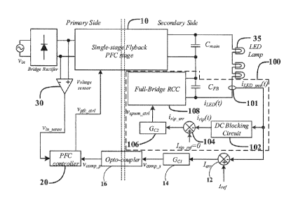
In the embodiment of Fig. 2A, the current ripple control loop 100, shown in
the dashed
box, includes a load current (AC and DC) sensing circuit 101, a DC blocking
circuit 102, a
subtractor 104, a compensation network (Gc2) 106, and a fall-bridge RCC 108
with output
capacitor CFB. Operation of the current ripple control loop is as follows: the
double-line-
frequency current ripple (irip) is sensed by blocking the DC component of the
LED current (iLED)
and is subtracted from a non-ripple reference (Trip_õf¨ 0) at 104, generating
an error signal (i
K-rip_err).
Based on this error signal, the compensation network 106 produces a sinusoidal
pulse width
modulation (SPWM) control signal (vsp,,,,Lciri) to force the full-bridge RCC
108 to generate an out
of phase (i.e., inverted, 180 out of phase, or substantially 180' out of
phase) double-line-
frequency voltage ripple. Series connection of the full-bridge RCC output and
the PFC output
cancels the double-line-frequency voltage ripple in the PFC output, resulting
in an LED current
(iLED(0) that is ripple-free (trip= 0) or substantially ripple-free (trip 0).
That is, the double-line-
frequency component in the LED current is significantly reduced or eliminated.
It is noted from Fig. 2A that both the PFC controller 20 output (viy,clrl,1 _
and the output
from the compensation network 106 (vsp,,,,m_ca-i) are based on the LED current
(iLED), rather than the
output voltage signals. Therefore, the PFC controller 20 and the full-bridge
current ripple
cancellation converter 108 may share the same LED current sensing circuit 101.
In a practical
implementation, to avoid the negative part of the sensed AC current ripple
signal, a level shifter
(e.g., a DC bias, /bias) may be applied to both the sensed current ripple
(trip) and its reference. An
example of this is shown in the embodiment of Fig. 2B, which also shows
further details of the
control loop 100, wherein the series full-bridge RCC 108 is implemented with a
floating capacitor
RCC. In particular, a current sensing network is shown at 101 and a DC
blocking and level shift
circuit are shown at 102. The DC bias ('bias) is shown at 103a and 103b. Fig.
2B also shows an
SPWM generator 107 that receives the control signal ctrl) and generates the
gating signals
for the switches of the full-bridge RCC.
In various embodiments, the series RCC may be implemented with any DC-DC
converter
or DC-AC inverter, such as a fall-bridge, buck, flyback, boost, buck-boost,
etc. Where a full-
bridge converter is used, it may be a floating capacitor implementation.
- 7 -
CA 02998288 2018-03-09
WO 2017/045075 PCT/CA2016/051085
Fig. 3 shows another embodiment of the current-ripple-based control strategy
as applied to
an LED driver, using an isolated single-stage flyback PFC stage 40, where a
floating capacitor
full-bridge inverter 208 is used as the series RCC (shown in the dashed box).
Fig. 4 shows an
embodiment of a current ripple control loop for the floating capacitor series
RCC 208, including a
subtractor 204, compensation network 206, and SPWM generator 207. Details of a
DC blocking
circuit 210 and an AC ripple sensing and level shift circuit 212 are also
shown. Compared to the
prior approach shown in Fig. 1B, the current-ripple-based control strategy
simplifies the control
circuit by removing two differential sensing single-ended voltage conversion
circuits.
According to the control strategy, the full bridge RCC provides an inverted AC
voltage
ripple to cancel the double line frequency current ripple in the LED output
current. The peak to
peak value of the main stage's output ripple voltage Vripple may be evaluated
via the LED current,
/LED, and the output capacitance, Cmain, as shown in equation (1).
= Pin 'LED
(1)
rqpe W X Ci XVLED 2n- x f x Cmain
man
An LED may be a single LED chip or lamp or may comprise two or more LED chips
or
lamps connected together (e.g., in series, parallel, or series-parallel). Fig.
5A shows a LED string
as a load, and the linear model of each LED chip is shown in Fig. 5B. The
model includes an
equivalent voltage source (Vfwd) in series with an ideal diode and a small
resister (RLED). The
relationship between the LED voltage and the current is dependent on the
characteristics of the
LED load, and is expressed in equation (2). The resistance and forward voltage
of a LED load is
dynamic with the forward current, but can be considered constant for a given
average output
current.
The relationship between the LED voltage and current ripple is expressed in
equation (3).
I
VLED _string ¨ nVd
= fiv
LED (2)
nRLED
AV
LED _string
AI LED (3)
nR.LED
Given the low equivalent resister characteristic as well as the nonlinearity
of the LED
load, even a small LED voltage ripple (z VLED_ string) may result in a large
LED current ripple
(AILED). This presents a challenge for the prior strategy shown in Fig. 1B,
since it is difficult to
- 8 -
CA 02998288 2018-03-09
WO 2017/045075 PCT/CA2016/051085
cancel the current ripple by limiting the voltage ripple when the voltage
ripple is too small to be
detected.
In addition, compared to the prior voltage-ripple-based cancellation method
requiring two
differentially sensed voltage signals, current-ripple-based embodiments only
sense the current
ripple and compare it to a zero reference (a DC voltage), avoiding an error
due to a mismatch
between the two sensing circuits (as in Fig. 1B), and thus leading to a more
effective solution to
cancel the current ripple.
In order to accommodate different LED-load combinations, the driver must
handle a wide
output voltage range under the rated output current. The ratio of the highest
output voltage over
the lowest output voltage is usually higher than 1.5 times (e.g., VLED= 90 ¨
150 V). With prior
ripple cancellation technologies, given the auxiliary winding turns ratio is
fixed, the component
voltage rating has to be overdesigned under the low output voltage operation
(e.g., VLED< 150 V)
to fit the voltage stress at the highest output voltage operation (e.g., VLED=
150 V), resulting a
non-optimal solution in terms of the component voltage stress as well as the
flyback RCC
efficiency.
As to the ripple cancellation embodiment with a floating capacitor (Figs. 3
and 4), the
peak-to-peak value of the double line frequency voltage ripple in the PFC
output, Vripple, is only
proportional to the LED output current 'LED as well as the PFC output
capacitance Cm., given the
line frequencyfEne is fixed. Therefore, the voltage stress of the floating
capacitor is
designed based on the highest LED current 'LED as the worst case and can be
reduced close to but
slightly higher than the peak voltage ripple at full load. However, since the
floating capacitor
voltage is regulated and fixed, the floating capacitor voltage may be much
higher than the peak of
the low frequency voltage ripple under a light LED current load, resulting in
unnecessary loss in
the flyback RCC.
The current-ripple-based control embodiments can achieve optimization of
ripple
cancellation with the minimum floating capacitor voltage regardless of the LED
output voltage
(VLED) and loads ('LED). The circuit operation is as follows, with reference
to Figs. 3 and 4. The
flyback RCC (FBRCC) input voltage Vaux is initially charged to exceed the peak
value of Vrippte by
'LED due to its unidirectional flowing characteristic, and then the voltage
starts decreasing due to
the loss in the FBRCC. This results in V. being less than Vrippk where the
sinusoidal peaks are
lost. The resulting LED current presents a small drop (less than its nominal
value) at each valley
- 9 -
CA 02998288 2018-03-09
WO 2017/045075 PCT/CA2016/051085
of v. The small distortion makes the RCC consume less energy during each
positive half cycle
than that it receives during each negative cycle, offsetting the RCC loss. The
current bumps are
fixed when the energy saved by the distortion equals to total RCC loss in each
120 Hz cycle. As a
result, the RCC input voltage is auto-tuned and kept very close to but a bit
less than the peak
value of the output voltage without an extra input voltage regulation loop.
Since the FBRCC loss
is in proportion to its input voltage (given the fixed output AC voltage),
with the current-ripple-
based method the FBRCC component voltage stress and the loss are minimized.
In practical implementations, power loss of the RCC may result in instances
where the
RCC input voltage is lower than the 120 Hz voltage peak of the PFC output when
the PFC output
voltage reaches its peak value. When this happens the RCC cannot tightly
follow the ripple
peak, since the RCC's output voltage is higher than its input voltage. As a
result, bumps may
occur at 120 Hz in the output current, a phenomenon referred to herein as
"under-cancellation",
shown in Fig. 8B
The under-cancellation phenomenon may be overcome by using a double-loop
control
method, wherein a slow voltage control loop is provided to regulate the ripple
cancellation
converter output voltage (average value), in addition to the fast current
ripple cancellation loop.
With the slow voltage loop regulating the average output voltage, the output
voltage is always
lower than the input voltage of the RCC. Therefore, the RCC is able to
generate a DC voltage
with an out-of-phase voltage ripple that substantially or completely cancels
the 120 Hz ripple
component in the PFC output voltage.
Fig. 6 shows an embodiment including a flyback PFC stage 50 that uses a buck
converter
as the RCC 308, as an example of an implementation of the double loop current
ripple sensing
method, and Fig. 7 is an embodiment of a control scheme with slow and fast
control loops. Fig.
8A shows typical waveforms. As can be seen in the embodiment of Fig. 7, the
slow PI loop is
used to regulate the average value of the ripple cancellation circuit output
voltage. At 314 the
sensed output voltage (Vo_buck_avg) is compared to the reference
(Vo_buck_avg_fef) to produce an error
signal that is fed to the slow PI 316 and a DC control voltage (vetra(t)) is
generated. The fast PI
loop is used to cancel the 120 Hz current ripple in the LED current. The
double line frequency
current ripple (irip(t)) is obtained by blocking the DC component of the LED
current (iLED) at 310
and sensing at 312, optionally with a DC offset ('bias). The current ripple
ir,p(t) is compared to a
non-ripple reference ('rip _ref¨ 'bias) at 304, which generates an error
signal (irip_err(t)). Based on
- 10 -
CA 02998288 2018-03-09
WO 2017/045075
PCT/CA2016/051085
this error signal, the fast PI 306 produces control output vetrn(t). The two
control outputs are
subtracted at 320 to produce vart_sum which is compared to a saw-tooth wave at
322 to generate
the driving signal at 324 for the ripple cancellation circuit 308. Thus, the
driving signal is
regulated to force the ripple cancellation circuit 308 to generate an inverse
double-line-frequency
voltage ripple on the regulated average voltage. The output voltage across the
LED load will be
the sum of the PFC stage 50 output and the ripple cancellation stage 308
output. As a result, the
double-line-frequency component in the LED current (iLED(t)) is significantly
suppressed and the
LED current is substantially ripple-free (irip = 0).
An advantage of the current ripple sensing RCC embodiments and the double-loop
current ripple sensing RCC embodiments is that there is no mismatch problem
for the sensing
circuit, because the sensed output ripple information is compared to a DC
reference directly,
rather than an AC voltage reference (i.e., sensed PFC ripple). Since the DC
reference is of high
accuracy (i.e., a stable, constant DC value), the ripple cancellation
perfoimance is improved.
The double-loop current sensing ripple cancellation strategy avoids the 120 Hz
ripple in
.. the output caused by the under cancellation phenomenon described above
(e.g., Fig. 8B). With
the average output voltage being regulated, the average output of the PFC
stage Vo_pfc avg (e.g.,
implemented with a buck converter) is fixed at VLED-Vo_buck avg, and the under
cancellation
phenomenon is avoided as long as the input voltage of the buck converter Vin
_buck is higher than
the buck output voltage Vo_buck.
Embodiments will be further described by way of the following non-limiting
examples.
Example 1
An experimental 100 W LED driver was built according to the parameters in
Table 1 .
Table 1. LED Driver Parameters
Specifications of LED driver ____________________________________________
Line input voltage (vin) 85-265V
LED output voltage (VLED) 90-150V
Rated LED output current ('LED) ___________________________ 0.67A
Rated power (Po) 100W
Line frequency (r) _________________________________________ 60Hz
-11 -
CA 02998288 2018-03-09
WO 2017/045075 PCT/CA2016/051085
Table 1. (continued)
Active Clamp SingIe-stage Flyback PFC Stage
Output Capacitor (Crnain) 56 F (250V Film Cap)
Switches (Q
main ,r_aux, SPP11N80C3
Diode (D) C3D16060
Turns Ratio (Np:Ns) 1.2:1 __________
Magnetizing Inductance (Li) 1300 p.H
Internal Leakage Inductor (Liek) 33 p.H
External Leakage Inductor (Lext) 15 pH
__________ Active Clamp Capacitor (Cdan,p) 470 nF (400V Film Cap)
Single-stage PFC Controller NCP1652A
________________________________________________________________________ FB
RCC Stage --
Switching Frequency (kw) 156 KHz __
Fx12
Input Floating Capacitor (Caux)
(50V 1206 Ceramic Cap) __________________________________________________
Output Inductor (LFB) 22 RH
4.7 Fx1
Output Capacitor (CFB)
(50V 1206 Ceramic Cap) __________________________________________________
TPN11003NLLQx4
Full-bridge Switches (Qi¨Q4)
(30V, 11m,c2)
LED String Load
XMLEZW-02-0000-0BOOT527F
LED Chip Part Number (15-27pcs for different load
combination)
Forward Voltage/pcs (V1) Typ _________________________ 6 V
Max Current (L.) 2 A
Luminous Flux/pcs @ 670 mA __________________________________ 270 lm
Figs. 9A and 9B show that the prototype produced only a very small LED driving
voltage
ripple @120 Hz (0.23 V RMS when VLED= 150 V; 0.12 V RMS when VLED= 90 V) with
only
60.7 p.F total output capacitance (Cmain+ CEB). According to Equation (1),
when using
5 conventional single-stage LED drivers, such a small ripple voltage can be
only achieved when the
output capacitance is increased to 2760 jiF. Therefore, the total required
output capacitance of the
single-stage driver was reduced by 97.8%.
Figs. 10A and 10B show the same 37 V ripple of the main stage (CH1) at the
same LED
current (CH4, 0.67 A) but at different LED voltages (VLED= 150 V in Fig. 7A
and VLED= 90 V in
10 Fig. 10B). Figs. 10A, 10C, and 10D show the different main stage voltage
ripples (CH1)
corresponding to the different LED currents (CH4) at the same LED voltage
(VLED= 150 V). As
- 12-
CA 02998288 2018-03-09
WO 2017/045075 PCT/CA2016/051085
described above, with small bumps occurring on the LED output current, the
average value of
input voltage Vc:
aux (CH3) is auto-tuned close to the peak values of CH1 (FBRCC output voltage,
vFB) under all the given conditions: Fig. 10A: VLED= 150 V, /LED= 0.67 A; Fig.
10B: VLED= 90 V,
ILED¨ 0.67 A; Fig. 10C: VLED= 150 V, 'LED = 0.4 A; Fig. 10D: VLED = 150 V,
ILED= 0.2 A.
Accordingly, the voltage stress on the RCC components is reduced and the RCC
efficiency is
improved.
Under universal AC input the experimental prototype shows a system efficiency
of 91% at
vu = 110 Vac and 92% at vin = 220 Vac, and a peak system efficiency of 92.5%
(Fig. 12A). The
PF over the range of input voltage (85 ¨ 265 Vac) is shown in Fig. 12B. Figs.
11A and 11B show
the input voltage and input current waveforms at vin = 110 Vac and 92% at vin
= 220 Vac,
respectively, and corresponding power factors of 0.99 and 0.96. The FBRCC
stage loss was
generally less than 1% under a range of input voltage, as shown in Fig. 13.
Dimming
performance of the LED driver is shown in Figs. 14A and 14B. Under the nominal
input voltages
of 110 Vac and 220 Vac, the half-load (Po= SOW, VLED Z 150 V) system
efficiency is generally
higher than 88.5% and the PF is over 0.9.
Example 2
A simulation model of a 240 W continuous current mode (CCM) single-stage
flyback
LED driver with buck ripple cancellation circuit was built in PSIM (version
9.1.3, Powersim
Inc., Rockville, MD). The design specifications are shown in Table 2 and the
circuit parameters
are given in Table 3.
Table 2. Specifications of LED driver for PSIM simulation
Vitt VLED 'LED PO June
=
85 Vac 60 Vdc 4A 240 W 60 Hz
- 13 -
Table 3. Circuit parameters for LED driver for PSIM simulation
Active Clamp Single-Stage Flyback PFC Stage
Output Capacitor (Cmcnn) 470 [IF
Turns Ratio (Np:Ns1:Ns2) 6:5:1
Magnetizing Inductance (Lm) 1300 [tH
Leakage Inductance (Lick) 33 [tH
External Leakage Inductor (Lext) 15 [tH
272 nF
Active Clamp Capacitor (Cc/amp)
(68 nFx4, 400V Film Caps)
Buck RCC with double-loop current-ripple-sensing ripple cancellation
Switching Frequency (fsw) 200 KHz
Input Capacitor (Caux) 120 [IF
Input voltage (Vaux) 30 V
Output Inductor (LFB) 22 [tH
Output Capacitor (CFB) 10 F
The simulation results are shown in Figs. 15A and 15B. In Fig. 15A it can be
seen that
the AC voltage generated by the buck ripple cancellation stage (Vbuck ripple)
mitigates the 120 Hz
PFC ripple (VpFC ripple), resulting in a flat voltage (\TEED). This
corresponds to a flat LED current.
The 120 Hz PFC voltage ripple is 23V pk-pk before cancellation. Fig. 15B shows
that the LED
output voltage ripple at 120 Hz is only 0.65 V after cancellation.
Fig. 16 shows the simulation results of input current and input voltage, when
Vin = 85
Vac, VLED = 60 V, kED = 4A, PO = 240W. The power factor is 0.993.
Equivalents
Those skilled in the art will recognize or be able to ascertain variants of
the embodiments
described herein. Such variants are within the scope of the invention and are
covered by the
appended claims.
-14-
Date Recue/Date Received 2021-09-14