Note: Descriptions are shown in the official language in which they were submitted.
84225996
STRUCTURES AND METHODS FOR CONTROLLING LOSSES IN PRINTED
CIRCUIT BOARDS
[0001]
FIELD
[0002] Embodiments described herein are generally related to the field of
reducing
losses in printed circuit board devices. More specifically, embodiments as
disclosed herein are
related to the field of winding loss management in stators made on multi-layer
printed circuit
boards for electric motors and/or generators.
BACKGROUND
[0003] The inventor has recognized and appreciated that current electric
motors and
other electric devices handling high currents through electrical leads in a
printed circuit board
(PCB) face multiple problems resulting from the electrical current flow in the
PCB. Such
problems include the generation of unwanted heat due to parasitic or eddy
currents, which can
lead to mechanical failure and destructive mechanical interferences with the
rotor of the motor
or generator, as well as other inefficiencies in the operation of the motor or
generator. As a
byproduct of the increased current density flow in regions of the electrical
circuit, high
temperature gradients in the PCB caused by, inter alia, high electrical
current gradients may
lead to structural damage of the PCB, such as delamination, or localized
failure or degradation
of the electrical leads or the dielectric material in the substrate. More
importantly, perhaps,
Date Recue/Date Received 2021-07-30
CA 03000002 2018-03-26
WO 2017/059257
PCT/US2016/054794
these high electric current densities act to generate undesirable larger
electromagnetic fields
which can create, for example, parasitic and eddy currents in physically
nearby regions of the
electric circuits, which in turn can act as a drag on the motor Or generator
rotor and thereby
reduce its power output and efficiency.
[0004] Printed circuit board electric devices built without the advantageous
features
described hereinafter, employ a variety of strategies to make connections
between electrical
current carrying traces laid down on the PCB surface, or surfaces in the case
of a multilayer
board device, of the dielectric substrates found in these devices. These
strategies, however, do
not address, or recognize in any substantial way, the disadvantages resulting
from enhanced
current density in portions of the electric circuit traces and the adverse
results therefrom.
SUMMARY
[0005] A particular example embodiment of the disclosure relates to printed
circuit
board motors and generators. Windings formed from copper in printed circuit
boards have been
used for purposes of forming antennas, inductors, transformers, and stators
that can be
incorporated in permanent magnet brushless DC (permanent magnet synchronous)
machines.
For energy conversion devices using modern permanent magnet materials and PCB
stators, the
magnetic field is not strongly confined by magnetically susceptible materials.
Thus, the
interaction between fields from adjacent turns in a winding, and/or windings
on adjacent layers
(for a multilayer configuration) may be significant. The structures disclosed
hereinafter reduce
the effective resistance in the windings, and therefore reduce the associated
losses to achieve a
specified current density in rotating energy conversion devices. The effect of
the disclosed
structures is a measurable reduction in loss mechanisms as a function of
increasing frequency,
compared to the currently available devices. These effects are significant in
frequency ranges
important to energy conversion processes as well as typical control
strategies, for example,
pulse-width modulation.
[0006] In a first example embodiment, the disclosure relates to the structure
of an
electrical motor or generator stator which includes a planar composite
structure (PCS) having at
least one dielectric layer and a plurality of conductive layers. The PCS is
characterized at least
in part by a center origin point and a periphery. The stator can also include
a plurality of first
elements, radially extending conductive traces, which extend from an inner
radial distance rs to
2
CA 03000002 2018-03-26
WO 2017/059257
PCT/US2016/054794
an outer radial distance 2-1, the radii being measured from the center origin
point toward the
periphery of the PCS. The traces are generally angularly disposed on the PCS.
The plurality of
first radially extending elements are each connected at their inner and outer
ends to enable
winding loops, and other circuit structures, to be formed. When the elements
are connected in
such loops, the outer ends of the elements are connected using outer loop
interconnects and the
inner ends of the elements are connected using inner loop interconnects as
described in more
detail hereinafter. Further, according to some example embodiments of the
disclosure, at least
one of the first radial conductive elements is connected to at least one other
of the radial
conductive elements at their respective outer radius ends_ Also, first
conductive elements are
connected at their inner radius ends to other radially conductive elements.
There can result
plural closed loops having multiple windings and forming the stator, for
example, of an
electrical motor or generator.
[0007] A second example embodiment of the disclosure relates to an electrical
motor or
generator having a stator which includes a PCS with at least one dielectric
layer and at least one
conductive layer, the PCS being characterized at least in part by a center
origin point and a
periphery. The stator can also include a plurality of first electrically
conductive traces extending
radially from a starting radius, 7-0, from the center origin point toward the
periphery of the PCS
and disposed angularly on the PCS. A plurality of the conductive traces
connect through a
respective associated interconnect to at least one other conductive trace
extending radially from
an inner radius rofrom the center origin point radially outward toward the
periphery of the PCS
and disposed angularly from the associated conductive trace.
[0008] In another example embodiment, a stator has a planar composite
structure (PCS)
with at least one dielectric layer and a conductive pattern on a surface of
each said dielectric
layer. The conductive pattern has a plurality of first conductive traces, each
extending radially
from an inner radius to an outer radius and disposed angularly on one of the
dielectric surfaces,
with at least one of the first conductive traces connected at its outer radius
to at least one other
of the first conductive traces at its outer radius by a first interconnect.
The first interconnect is
bounded between inner and outer edges. The first interconnect has a starting
region, a transition
region, and an ending region, and the starting region has a first radiused
inner edge section
extending from the first conductive trace to the transition region, and the
ending region has a
second radiused inner edge section extending from the transition region to the
other conductive
trace; and wherein at least the first radiused inner edge section and the
second radiused inner
3
CA 03000002 2018-03-26
WO 2017/059257
PCT/US2016/054794
edge section is are each characterized at least in part by a Corner Equation,
_O¨Os
r(0) = rd + (rs ¨ rd)e a for a comer starting at Os and rs and evaluated for 0
> 0s, or the
equivalent reflected version with r(0) = rd + (rs ¨ rd)e-Os-0)/a for a corner
evaluated with
0 < Os and ending at Os and rs.
[0009] In yet another example embodiment, a stator has a planar composite
structure
(PCS) having at least one dielectric layer and a conductive pattern on a
surface of each said
dielectric layer. At least one conductive pattern has a plurality of first
conductive traces, each
extending radially from an inner radius to an outer radius and disposed
angularly on one of the
dielectric surfaces. At least one of the first conductive traces connected at
its outer radius to at
least one other of the first conductive elements at its outer radius by a
first interconnect, and
wherein at least the first interconnect is bounded by inner and outer edges,
and has a starting
region, a transition region, and an ending region, and the starting region has
a first radiused
inner edge section and a first radiused outer edge section extending from the
first conductive
trace to the transition region, and a second radiused inner edge section and a
second radiused
outer edge section extending from the transition region to the other
conductive trace. At least
the first radiused inner and outer edge sections and the second radiused inner
and outer edge
sections are each characterized at least in part by the Corner Equation r(0) =
rd +
_u-us
¨ rd) e a for a corner starting at Os and I's and evaluated for 0 > es, or the
equivalent
reflected version with
r(0) = rd + (r, ¨ rd)e-(0s- )/' for a corner evaluated with 0 < Os and ending
at Os and rs.
[0010] In another example embodiment, a stator has a planar composite
structure (PCS)
with at least one dielectric layer and a conductive pattern on a surface of
each said dielectric
layer. At least one conductive pattern has a plurality of first conductive
traces, each extending
radially from an inner radius to an outer radius and disposed angularly on one
of the dielectric
surfaces. At least one of the first conductive traces is connected at its
outer radius to at least one
other of the first conductive elements at its outer radius by a first
interconnect. The first
interconnect is bounded by an inner edge and an outer edge. The first
interconnect has a starting
region, a transition region, and an ending region, and the inner edge of the
starting region has a
first radiused inner edge section extending from the first conductive trace at
its outer radius to
the transition region, and a second radiused inner edge section extending from
the transition
region to the other conductive trace at its outer radius. At least the first
radiused inner edge
4
CA 03000002 2018-03-26
WO 2017/059257
PCT/US2016/054794
section and the second radiused inner edge section are each characterized by a
slope dr/de
which is a linear function of r(0) from the one conductive trace to the
transitional region and
where the slope is a different linear function from the transitional region to
the other conductive
trace.
[0011] In yet another example embodiment. a stator has a planar composite
structure
(PCS) comprising at least one dielectric layer and a conductive pattern on a
surface of each said
dielectric layer. At least one conductive pattern has a plurality of first
conductive traces, each
extending radially from an inner radius to an outer radius and disposed
angularly on one of the
dielectric surfaces. At least one of the first conductive traces is connected
at its outer radius to a
starting region of a first interconnect. The first interconnect is bounded by
inner and outer
edges, and the first interconnect having the starting region, a transition
region, and an ending
region, and a first radiused inner edge section extending from the outer
radius of the one
conductive trace to the transition region, and a second radiused inner edge
section extending
from the transition region to the other conductive trace at its outer radius.
At any point between
the inner and outer edge, the smallest current density magnitude under direct
current excitation
is not less than 50% of the largest current density magnitude evaluated along
the shortest line
between the inner and outer edge passing through that point.
[0012] In another example embodiment, a stator, has a planar composite
structure (PCS)
having at least two dielectric layers and a conductive pattern on a surface of
each said dielectric
layer. At least one conductive pattern has a plurality of first conductive
traces, each extending
radially from an inner radius to an outer radius and disposed angularly on
different ones of the
dielectric surfaces. At least one of the first conductive traces is connected
at its outer radius to
at least one other of the first conductive traces on a different surface at
its outer radius by a first
interlayer interconnect. The interconnect is substantially bounded by inner
and outer edges.
The first intcrlayer interconnect has a starting region on a first layer, a
transition region, and an
ending region on a different layer, and further has a first radiused inner
edge section extending
from a first conductive trace to the transition region, and a second radiused
inner edge section
extending from the transition region to the other conductive trace at its
outer radius; and wherein
at least the first radiused inner edge section and the second radiused inner
edge section are each
characterized at least in part by a structure designed to reduce parasitic and
eddy current effects
on axially adjacent conductive surface structures.
CA 03000002 2018-03-26
WO 2017/059257
PCT/US2016/054794
[0013] In a further example embodiment a stator has a planar composite
structure (PCS)
having at least one dielectric layer and a conductive pattern on a surface of
each the dielectric
layer. At least one conductive pattern has a plurality of first conductive
traces, each extending
radially from an inner radius to an outer radius and disposed angularly on one
of the dielectric
surfaces. At least one of the first conductive traces is connected at its
outer radius to at least one
other of the first conductive elements at its outer radius by a first
interconnect first interconnect
is bounded by inner and outer edges. The first interconnect has a starting
region, a transition
region, an ending region, and a first radiused inner edge section extending
from the connected
first conductive trace at its outer radius to the transition region, and a
second radiused inner
edge section connecting the transition region to the outer radius of the one
other conductive
trace. At least the first radiused inner edge section and the second radiused
inner edge section
are each characterized by a structure for reducing eddy currents in the outer
conductive portions
of the interconnect.
[0014] In yet another example embodiment, a stator has a planar composite
structure
(PCS) with at least one dielectric layer and a conductive pattern on a surface
of each said
dielectric layer. The at least one conductive pattern has a plurality of first
conductive traces,
each extending radially from an inner radius to an outer radius and disposed
angularly on one of
the dielectric surfaces; with at least one of the first conductive traces
connected at its outer
radius to at least one other of the first conductive traces at its outer
radius by a first interconnect,
the first interconnect bounded by inner and outer edges. The first
interconnect has a starting
region, a transition region, and an ending region, and first radiused inner
and outer edge sections
extending from the first conductive trace to its transition region, and second
radiused inner and
outer edge sections extending from the transition region to the one other
conductive trace at its
outer radius. At least the respective slope of the first radiused inner edge
section and the second
radiused inner edge section are each characterized by a monotonically changing
value of slope
as a function of the rotational angle from the one conductive trace to the
other conductive trace.
[0015] In a further example embodiment, a stator has a planar composite
structure (PCS)
with at least one dielectric layer and a conductive pattern on a surface of
each said dielectric
layer. At least one conductive pattern has a plurality of first conductive
traces, each extending
radially from an inner radius to an outer radius and disposed angularly on one
of the dielectric
surfaces, at least one of the first conductive traces being connected at its
outer radius to at least
one other of the first conductive traces at its outer radius by a first
interconnect. The first
interconnect is bounded by inner and outer edges. The first interconnect has a
starting region, a
6
CA 03000002 2018-03-26
WO 2017/059257
PCT/US2016/054794
transition region, an ending region, and a first radiused inner edge section
and a first radiused
outer edge section extending from the first conductive trace to the transition
region, and a
second radiused inner edge section and a second radiused outer edge section
extending from the
transition region to the one other conductive trace at the outer radius of the
other conductive
trace. At least between an inner edge section and an outer edge section of the
interconnect in its
transition region, the interconnect has at least one slit-like elongated
region that does not
substantially reduce electrical conductivity from one end of the interconnect
to the other end of
the interconnect, the slit-like elongated region extending substantially
parallel to the inner edge
section in the transition region of the interconnect.
[0016] In yet another example embodiment of the disclosure, a stator has a
planar
composite structure (PCS) having at least one dielectric layer and a
conductive pattern on a
surface of each said dielectric layer. At least one conductive pattern has a
plurality of first
conductive traces, each extending radially from an inner radius to an outer
radius and disposed
angularly on one of the dielectric surfaces. At least one of the first
conductive traces is
connected at its outer radius to at least one other of the first conductive
traces at its outer radius
by a first interconnect. The first interconnect is bounded at least by inner
and outer edges. The
first interconnect has a starting region, a transition region, and an ending
region, and a first
radiused inner edge section extending from the first conductive trace to the
transition region, and
a second radiused inner edge section extending from the transition region to
the one other
conductive trace at the outer radius of the other conductive trace. The inner
edge of the
interconnect from the connection between the first conductive trace and the
starting region to the
beginning of the transition region is designated the "CT inner edge" distance.
An example
embodiment achieves at least 90% of the maximum current density value, as
determined by
FEATEM calculations, within the first 20% of the CT inner edge measured along
the inner edge
of the interconnect from the first conductive trace toward the transition
region.
7
84225996
[0016a] According to an aspect of the present invention, there is provided an
apparatus, comprising: a planar composite structure (PCS) comprising at least
one
dielectric layer and a conductive pattern on a surface of the at least one
dielectric layer, the
conductive pattern comprising: at least first and second conductive traces,
each extending
radially from an inner radius to an outer radius and disposed angularly on the
surface; and
a first interconnect having a first portion connected to the first conductive
trace at the outer
radius and a second portion connected to the second conductive trace at the
outer radius;
wherein the first interconnect is bounded by an inner edge and an outer edge,
and has a
starting region, a transition region, and an ending region, the starting
region having a first
radiused inner edge section extending from the first conductive trace to the
transition
region; and wherein at least a portion of the first radiused inner edge
section has a
curvature that varies continuously as a function of r and 0.
10016b] According to another aspect of the present invention, there is
provided an
apparatus, comprising: a planar composite structure (PCS) comprising at least
one
dielectric layer and a conductive pattern on a surface of the at least one
dielectric layer, the
conductive pattern comprising: at least first and second conductive traces,
each extending
radially from an inner radius to an outer radius and disposed angularly on the
surface; and
a first interconnect having a first portion connected to the first conductive
trace at the outer
radius and a second portion connected to the second conductive trace at the
outer radius;
wherein the first interconnect is bounded by an inner edge and an outer edge,
and has a
starting region, a transition region, and an ending region, the starting
region having a first
radiused inner edge section extending from the first conductive trace at the
outer radius to
the transition region, and a second radiused inner edge section extending from
the
transition region to the second conductive trace at the outer radius; and
wherein at least the
first radiused inner edge section and the second radiused inner edge section
are each
characterized by a slope dr/d0 which is a linear function of r(0) from the
first conductive
trace to the transition region and where the slope dr/d0 is a different linear
function from
the transition region to the second conductive trace.
[0016c] According to still another aspect of the present invention, there is
provided
an apparatus, comprising: a planar composite structure (PCS) comprising at
least one
dielectric layer and a conductive pattern on a surface of the at least one
dielectric layer, the
conductive pattern comprising: at least first and second conductive traces,
each extending
7a
Date recue / Date received 2021-12-10
84225996
radially from an inner radius to an outer radius and disposed angularly on the
surface; and
a first interconnect having a first portion connected to the first conductive
trace at the outer
radius and a second portion connected to the second conductive trace at the
outer radius;
wherein the first interconnect is bounded by an inner edge and an outer edge,
and has a
starting region, a transition region, and an ending region, the starting
region extending
from the first conductive trace at the outer radius to the transition region,
and the ending
region extending from the transition region to the second conductive trace at
the outer
radius; and wherein at any point between the inner and outer edge, a smallest
current
density magnitude under direct current excitation is not less than 50% of a
largest current
density magnitude evaluated along a shortest line between the inner and outer
edge passing
through that point.
[0016d] According to yet another aspect of the present invention, there is
provided
an apparatus, comprising: a planar composite structure (PCS) comprising at
least one
dielectric layer and a conductive pattern on a surface of the at least one
dielectric layer, the
conductive pattern comprising: at least first and second conductive traces,
each extending
radially from an inner radius to an outer radius and disposed angularly on the
surface; and
a first interconnect having a first portion connected to the first conductive
trace at the outer
radius and a second portion connected to the second conductive trace at the
outer radius;
wherein the first interconnect is bounded by an inner edge and an outer edge,
and has a
starting region, a transition region, and an ending region, the starting
region having first
radiused inner and outer edge sections extending from the first conductive
trace at the
outer radius to the transition region, and second radiused inner and outer
edge sections
extending from the transition region to the second conductive trace at the
outer radius; and
wherein at least a respective slope of the first radiused inner edge section
and outer edge
section and the second radiused inner edge section and outer edge section are
each
characterized by a monotonically changing value of slope as a function of a
rotational
angle from the first conductive trace to the second conductive trace.
7b
Date recue / Date received 2021-12-10
CA 03000002 2018-03-26
WO 2017/059257
PCT/US2016/054794
BRIEF DESCRIPTION OF THE DRAWINGS
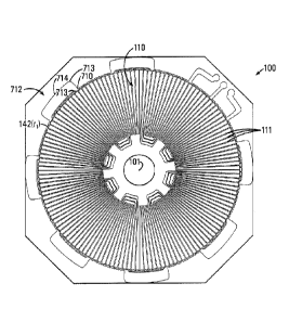
[0017] Figure 1 illustrates a plan view of a stator including a PCS having at
least one
dielectric layer with one of a plurality of conductive layers being
illustrated in accordance with
some embodiments of the disclosure;
[0018] Figure 2A is a black-and-white copy of a color illustration of an FEM
solution for
current density in an end-turn corner with sharp corners;
[0019] Figure 2B is a grayscale version of the FEM solution shown in Fig. 2A;
[0020] Figure 3A is a black-and-white copy of a color illustration of an FEM
solution for
current density in an end-turn corner structure with radius corners wherein
the radius
corresponds to the half-width of the smaller trace;
[0021] Figure 3B is a grayscale version of the FEM solution shown in Fig. 3A;
[0022] Figure 4A is a black-and-white copy of a color illustration of an FEM
solution for
current density in accordance with an example embodiment of the disclosure;
[0023] Figure 4B is a grayscale version of the FEM solution shown in Fig. 4A;
[0024] Figure 5 illustrates a plan view of a stator including a PCS in
accordance with a
prior art structure having sharp corners;
[0025] Figure 6 illustrates a plan view of a stator including a PCS wherein
the corners
have a constant turning radius;
[0026] Figure 7 illustrates details of an outer loop connection in a stator,
each connection
configuration including a first starting region connecting to a transition
region connecting in turn
to a termination region, according to some embodiments of the disclosure;
[0027] Figure 8 illustrates a greatly expanded, in the z axis, motor stator
stack up;
[0028] Figure 9 illustrates an end turn loop having an interconnecting trace
which is split
longitudinally;
8
CA 03000002 2018-03-26
WO 2017/059257
PCT/US2016/054794
[0029] Figure 10A is a black-and-white copy of a color illustration of an FEM
solution
showing a resulting current density without the narrow elongated slit-like
regions illustrated in
Figure 9;
[0030] Figure 10B is a grayscale version of the FEM solution shown in Fig.
10A;
[0031] Figure 11A is a black-and-white copy of a color illustration of an FEM
solution
showing a resulting current density with the narrow elongated slit-like
regions illustrated in
Figure 9;
[0032] Figure 11B is a grayscale version of the FEM solution shown in Fig.
11A;
[0033] Figure 12 illustrates a cross-sectional view of a section of stator 100
according to
some embodiments;
[0034] Figure 13 illustrates a detail of stator 100 including a plurality of
conductive
elements 111 disposed on the PCS;
[0035] Figure 14 illustrates a detail of an inner area of the stator proximal
to the center
origin point;
[0036] Figure 15 illustrates a perspective view of connection configurations
according to
some embodiments of the disclosure; and
[0037] Figure 16 is a flow chart in a method for manufacturing a stator
including a
planar composite layer (PCS) having at least one dielectric layer and a
plurality of conductive
layers, according to some embodiments.
[0038] In the figures, elements and steps denoted by the same reference
numerals are
associated with the same or similar elements and steps, unless indicated
otherwise.
DETAILED DESCRIPTION
[0039] Referring to Figure 1, in an example embodiment of the disclosure, a
plan view
of a stator 100 for use in an electrically driven motor or a rotating
generator, has a planar
9
CA 03000002 2018-03-26
WO 2017/059257
PCT/US2016/054794
composite structure (PCS) 110 with at least one dielectric layer and a
plurality of substrate
layers having conductive traces 111 thereon. The diameter of the stator shown
in Figure 1 can
be on the order of cm to tens of meters. Conductive traces 111 can be part of
a winding
structure in accordance with an embodiment of the disclosure that can be
connected at the outer
annulus and inner section of a PCB structure. PCS 110 is characterized at
least in part by a
center origin point 101 and an outer periphery 102. Stator 100 includes a
plurality of first
conductive traces 111 extending radially from a radius 140 (ro) (measured from
the center origin
point 101) to a radius 142 (r1) (measured from center origin point 101) toward
periphery 102 of
PCS 110 and disposed angularly on the PCS_ One or more of the first conductive
traces are
connected at their outer end, at radius r1, to typically one or more other of
the first conductive
trace(s) at its outer radius ri. Such an interconnect, designated as an outer
loop, has a starting
region 144, a transition region 148, and an ending region 150.
[0040] In a complementary manner, a plurality of the conductive traces are
connected at
their inner ends, at radius ro, by inner conductive loops 151, each inner
conductive loop
similarly having a starting region, a transition region, and an ending region.
In this manner, the
combination of conductive traces 111, and their connecting structures, provide
for a winding
structure on the surface(s) of the dielectric layer(s).
[0041] In more complex structures, the conductive traces 111 can be connected
to
conductive traces on other layers using interior layer connections such as
vias or other interior
layer links. In these interlayer connections, the combination of the
conductive traces on each of.
for example, two (or more) layers combine to form an advantageous structure of
multilayered
windings as is well known in the field.
[0042] There is a concern, however, that the current passing from one
conductive trace
111 to the next conductive trace does not create electromagnetic fields which
may damage or
reduce the efficiency of the operating system of the motor or generator. Such
negative effects
can result, for example, in parasitic currents or eddy currents in nearby
electrically conductive
structures which can act as a drag on the system. As is explained further
below, such drag
reduces efficiency, and is not typically considered in the structural design
of the motor or
generator of Figure I. However the present disclosure is directed to reducing
substantially, by
proper shaping and design of the interconnecting end loops 151, 153, such
undesirable
electromagnetic fields.
CA 03000002 2018-03-26
WO 2017/059257
PCT/US2016/054794
[0043] Thus, a stator 100 may include multiple layers similar to the one
illustrated in the
planar view of Figure 1. The multiple layers may be arranged to provide a
sequence of coils or
windings that are connected, usually in series, to form the poles of a motor
or generator. The
poles are then typically segregated into groups, with at least one group for
each phase of current
supplied to the motor (or generated by the generator). Collectively, when
properly controlled by
an external electric circuit, the arrangement of conductors (for example,
traces 111, and
interconnecting conductive traces 151 and 153 in PCS 110) creates a rotating
current density
and associated magnetic field. This rotating current density (and magnetic
field) can exert a
torque on a surrounding magnetic structure (for a motor) or generate a current
output (for a
generator). The part of the printed circuit board with the radial structures
111 (the -active area")
is the part of the stator designed to participate in this interaction.
Accordingly, the active area of
stator 100 may include conductive traces 111 coupled through interconnecting
conductive traces
151 and 152 to form the rotating current. Some embodiments include two sets of
rare-earth
magnets fixed to a shaft passing through the center origin point 101 of PCS
110, which forms a
compact, high-efficiency axial field synchronous electric device. In addition
to the active area
including a rotating current density that interacts with an inhomogeneous
magnetic field, stator
100 may include conductive elements in a peripheral area and conductive
elements in an interior
area. Conductive elements and can dissipate heat generated by stator 100,
while in operation.
[0044] In accordance with the structure of the disclosure, a planar PCB, for
example, for
a rotary electrical motor or generator, has inner, outer. and neutral end-turn
structures which are
shaped to optimize stator performance. In a planar PCB motor stator, or planar
composite stator
(PCS), the end turn design is of critical importance for the simple reason
that end-turns serving
different roles in the winding plan usually cannot co-exist on a single layer,
and also cannot
appear on a large number of layers as a method of reducing their total
resistance. Another
consideration for end-turns is that they are in close proximity to other
conductive materials, for
example, other structures on the same or adjacent layers, which can lead to
eddy currents and
parasitic loads at
high frequencies.
[0045] The present disclosure addresses both issues, and can be compared to
other
design strategies and structures through use of finite element measurements
(FEM). The use of
"end-turn" in the following description should be understood to include
similar features in inner
11
CA 03000002 2018-03-26
WO 2017/059257
PCT/US2016/054794
and outer end turns, in links between pole groups, in cross-layer links, power
connections, and
in neutral tie-point structures. It is also important to recognize that while
a major use of the
technology disclosed herein is for no tears and generators, the application of
the technology to
any printed circuit board, single layer or multilayered, can be advantageous
for reducing losses
in the circuit. It is also important to note that within the motor/generator
field, the number of
end turns and their function will vary depending upon the number of phases,
turns, and the poles
for the motor.
[0046] As noted above, an inner or outer end turn has several connected
regions. The
basic functional part of an end-turn is a corner, a region that connects
electrical current from an
active region radial conductor or trace to a prescribed radius after the turn
or corner is executed,
typically changing the direction of the current on the planar surfaces from a
substantially
radially directed current to an angularly directed current. Often, the turn
connects to a narrow
width radial trace at its beginning connection point, the width of the
radially directed trace being
dictated by the spacing of conductors in the active region of the plane and
the space available for
the angular part of the turn. For purposes of illustration, and because the
feature under
consideration is approximately (locally) Cartesian, the angular travel in the
embodiments that
follow is indicated on the x-axis, while the radial travel is indicated on the
y-axis. There is a
conformal map between this case and the cylindrical coordinate case directly
applicable to the
PCS for axial field machines.
[0047] To explore the relationship between structure or shape of the end turn
design, and
its performance, FEM simulations of several example designed structures and
examples from
earlier designs are described with the condition that each structure carry
exactly the same total
current. Plots of current density magnitude within a structure were
subsequently produced from
the FEM solution, and are illustrated in Figures 2-4. The scales in these
plots arc adjusted so
that they can be compared. It should be appreciated that in the black-and-
white versions of the
color drawings presented herein (i.e., Figures 2A, 3A, 4A, 10A and 11A), the
darker regions do
not necessarily correspond to higher current density regions in the FEM
solutions and the lighter
regions do not necessarily correspond to lower current density regions in
those solutions. This
is true because the red and blue regions near the top and bottom,
respectively, of the scales for
the colored versions both copied as a darker color in the black-and-white
versions. Accordingly,
it is helpful to consider the grayscale versions of the FEM solutions (i.e.,
Figures 2B, 3B, 4B,
10B and 11B) in conjunction with the black-and-white copies of the colored
versions of those
12
CA 03000002 2018-03-26
WO 2017/059257
PCT/US2016/054794
solutions to better understand the relative current densities in the various
regions.
[0048] It is common for prior printed circuit board CAD packages to merge
lines of
different widths with square corners, as illustrated in Figure 5. End turns
with corners drawn
this way appear, for example, in United States patent 7,109,625. An adverse
consequence of
this structure, as shown in the FEM produced current density map in Figures 2A
and 2B, is that
the current is concentrated significantly at the inner corner 250 of the inner
edge section 251 of
the end turn. This creates a concentration of current, and hence energy loss
at the inner edge
corner, and the current is essentially zero at the outer corner edge 252. The
concentration of
current at the inner edge corner leads to a much stronger magnetic field H
(amperes per meter,
or Aim) in the immediate vicinity of the inner edge corner. The outer corner
copper serves
essentially no function in the conductivity of the structure, but by virtue of
proximity to the high
current density at the inner corner edge and other current sources on the PCS,
may present an
undesirable parasitic secondary to time-varying magnetic fields from such
other sources.
Further, the inner corner concentrates current and produces a magnetic field
that may
undesirably interact with other structures in the PCS. Collectively these
effects lead to increased
losses at higher frequencies, as well as a relatively higher resistance for
the amount of copper
used (because the copper at the outer edge of the corner carries substantially
no current, as noted
above)
[0049] The actual end-to-end conductivity of the structure in Figure 5 varies
in a
predictable fashion as a function of material conductivity, thickness, and
scale. For purposes of
comparison and to emphasize the importance of end-turn corner shape
independent of these
other variables, the conductivity of the structure in Figure 5 is designated
as 1.000.
[0050] It is important to note, for the Figure 5 shape/structure, that while
the current
entering the starting region 254 of the end turn is substantially uniform
across the entire cross-
sectional extent of the trace, in making the sharp turn it tends to congregate
inward.
[0051] Another common practice in CAD tools is to provide the option of
merging lines
with the application of a specified constant turning radius at the turn. Often
the radii at the inner
radiused corner 642 and outer radiused corner 645 used to replace the sharp
corner of Figure 5
are chosen based on the widths of the lines to be merged. The geometry of the
corner illustrated
in Figure 6 shows this type of end turn corner. Note that in Figure 6, there
are 3 nested end
13
CA 03000002 2018-03-26
WO 2017/059257
PCT/US2016/054794
loops 635. In this case, the inner and outer radii for inner edge 640 and
outer edge 650 are the
same as the radius of the aperture used for the vertical trace segment. The
operation of the
structure illustrated in Figure 6 is improved relative to the structure
illustrated in Figure 5 (as
shown by the FEM simulation of Figures 3A and 3B), although the Figure 6
structure/shape still
shows current concentration near the inner corner edge, and some copper at the
outer corner
edge still does not carry significant current. The conductivity of the
structure illustrated in
Figure 6 relative to Figure 5 is 1.046. The structure of Figure 6 therefore
provides less
resistance loss; however, the current density is still undesirably high at the
inner corner edge
resulting in the same undesirable effects noted in connection with the
structure of Figure 5.
albeit at slightly lower levels.
[0052] An example embodiment described herein thus recognizes the need to
obtain a
further reduction from the high current densities of the earlier structures
illustrated in Figures 2
and 5, and Figures 3 and 6, to determine a design shape and function which
significantly reduces
the concentration of current density along the inner corner, and specifically
the inner corner
edge, with the consequent reduction of the negative effects resulting from the
high concentration
of current density illustrated in Figures 2 and 3.
[0053] Referring to Figure 7, the end-turn structure illustrated there is
bounded by its
inner and outer edges, and corresponds to a local solution of a first-order
differential equation in
x and y (or rand 0). This example and preferred embodiment, corresponding to a
single-
variable parameterization of a continuous transition from the starting width
and location 710 of
the end-turn corner 712, through the corner, to the x or theta directed
portion 714 of the end
turn. The smooth transition described in more detail below avoids the
localized concentration of
current in the corner transition found in the Figures 5 and 6 examples and
does not tend to
concentrate the current density in the turn. Accordingly the undesirable
magnetic fields
produced by earlier structures (Figures 5 and 6) are minimized. The
parameterization of the turn
provides an independent variable that can be used for optimization purposes in
different designs.
As illustrated in Figure 4, this end turn design avoids concentration of
current density and
magnetic field and has a relative conductivity of 1.197, almost 20% higher
than the end-turn
structure illustrated in Figure 5. Further, in one particular example
embodiment of the
disclosure, the inner and outer edges can be shaped in accordance with the so-
called -Corner
equation":
_9-9s
r(0) = rj + (r, ¨ rd)e a for a corner starting at 0, and r, and evaluated for
14
CA 03000002 2018-03-26
WO 2017/059257
PCT/1JS2016/054794
0 > 0s, or the equivalent reflected version with r(0) = rd + (r, ¨ rd)e-( s-
)/a
for a corner evaluated with 0 < 0, and ending at 0, and rs. This equation
provides for a
gradual change of the radius of curvature along the edges and is controllable
by a single
parameter, a, selected depending upon the beginning and end points of the
edge. In a preferred
embodiment, the slope is a continuously changing variable having a zero second
derivative.
This is equivalent to saying that the radiuscd edge is characterized by a
slope, which is a linear
function of r from the starting point, (the intersection between the starting
region and the
conductive trace) to the transition region and that the slope is a different
linear function from the
transitional region to the end of the ending region. The entire loop edge
structure can be
described from initiating trace 111 to final trace 111 by a single equation:
_0-01 / \
r(0) -= rsi + Olt ¨ 7'11) (1 e \ (1'32 ¨ rct) V a )
where n1, el is the starting point of the structure at the initiating trace
111, n2, e2 is the ending
point of the structure, a is the parameter of the corners, and rd is the
radius at which the
structure extends primarily in the angular direction.
[0054] The avoidance of a concentration of current density in the loop (inner
or outer)
can be viewed by measuring the current density along the inner edge of a loop
in the starting
region. Typically, the current density measurement will be higher in the
beginning of the
starting region where it connects to a conductive radial trace, and lowest at
the inner edge at the
intersection of the starting and transition regions. If the inner edge section
of the interconnect
from the connection between the first conductive trace and the starting region
to the beginning
of the transition region is designated the "CT inner edge" distance, then in
an example
embodiment, the current density achieves at least 90% of the maximum current
density value, as
determined by FEAIFEM calculations, within the first 20% of the CT inner edge
measured
along the inner edge of the interconnect from the first conductive trace
toward the transition
region. This differs substantially from the structures of Figures 5 and 6
wherein the peak occurs
much further away from the radial conductor at a location which more likely
adversely effects
parasitic and eddy currents in nearby conductors.
[0055] As noted above, the distance of a conductor to a source of
electromagnetic
radiation can significantly affect the strength of the electromagnetic field
impinging on the
CA 03000002 2018-03-26
WO 2017/059257
PCT/US2016/054794
conductor and its adverse consequences. This "proximity" effect is the
tendency for a current in
an adjacent conductor to influence the distribution of current in a primary
conductor, and vice
versa. This effect results in a change of current distribution in the primary
conductor as well as
losses in both conductors, and is apparent as an increase in the electrical
resistance of the
primary conductor as the current frequency increases. A closely aligned
concept is: the
tendency of a conductive material that is not part of the circuit at DC to
become a parasitic
"secondary" due to a current density induced by a time varying current in the
primary
conductor. This effect increases as (i) the frequency goes up, (ii) the
strength of the magnetic
field increases. and (iii) as the proximity of the parasitic conducting
material to the primary
decreases. These considerations mitigate in favor of both reducing the
concentration of the
electromagnetic field, for example, by using the example corner shape
structure illustrated in
Figure 7, and reducing the proximity of the conductor where possible to
adjacent conductors. In
a preferred example embodiment of the disclosure, the "corner equation"
specified hereinafter
helps ameliorate both of these effects.
100561 For either of the equations above, the parameter a determines the rate
at which
the end turn will approach its essentially constant radius, angularly
directed, portion of the stator
structure (the transition region). An important consideration is that the
corner needs to avoid
interference with nearby structures. If the nearby structures are nested
corners, such as those
described by the corner equation and illustrated at 153 in Figure 1, the outer
edge of an inner
end turn must be less than the "constant" radius of the inner edge of the
adjacent outer end
turn. Further, large values of a, may produce interference or minimum
clearance violations with
adjacent structures on the printed circuit board, such as termination
structures that are not
governed by the Corner Equation. With these considerations in mind, the
determination of a
suitable value of a can be inferred from the angular displacement (designated
as 8) of two
adjacent radial traces 111 such as those shown in Figure 1. In a typical
stator, having for
example, 120 radial traces, the angular separation 8 may be, for example, on
the order of 30 (or
27c/120 radians) or less. Further, while a minimum fabrication clearance will
factor into a
precise calculation of the largest possible a for a given design, it is
undesirable to use an a that
is too large since the width of the complete end turn structure may be
reduced, with the effect of
increasing DC resistance of the structure. On the other hand, setting a to
values that are too
small, for example less than 0.18, effectively produces a square corner shape
and reduces the
advantages identified herein. Accordingly, a potential "range" for a where the
angular
16
CA 03000002 2018-03-26
WO 2017/059257
PCT/US2016/054794
separation between adjacent radial traces is, for example, between about 0.28
and 0.068 radians.
[0057] In addition to the Corner equation described above, there are other
descriptions
of forming and shaping the corner of an end loop or trace which also
ameliorate the effects seen
when the corner is "sharp." Thus, for example, as described above, and in the
context of an end
loop as described above in connection with, for example, and loop 714
illustrated in Figure 7,
the first radiused inner edge section and the second radiused inner edge
section of the endloop in
the starting and ending regions of the loop can each characterized by a slope
dr/de which is a
linear function of r(0) from a first conductive trace to the transitional
region and where the
slope is a different linear function from the transitional region to the
conductive trace to be
connected.
[0058] In another description of the forming and shaping of the corner of in
the end
loop, one can select any point between the inner and outer edge of the loop,
and shape the loop,
so that the smallest current density magnitude under direct current excitation
at that point is not
less than 50% of the largest current density magnitude evaluated along the
shortest line between
the inner and outer edge of the loop and passing through that point. This
approach accordingly
also reduces the adverse effects of aggregated current density.
[0059] In yet another description for forming and shaping the corner of an end
loop, the
respective slope of the first radiused inner edge section and the second
radiused inner edge
section of the loop are each characterized by a monotonically changing value
of slope as a
function of the rotational angle from the one conductive trace to the
conductive trace to be
connected. This also reduces induced currents by reducing the aggregated
current density at the
corner. In yet another approach to reducing aggregated current density, an
example embodiment
achieves at least 90% of the maximum current density value, as determined by
FEA/FEM
calculations, within the first 20% of the CT (as defined above) inner edge
measured along the
inner edge of an interconnect from the first conductive trace toward the
transition region.
[0060] In practical stator designs, out-of-plane structures may also form
parasitic
secondary elements. Figure 8 shows a greatly expanded (in the z-axis)
rendering of a motor
stator stack up. In actual construction, the spacing between copper would be
roughly the same
as the copper thickness. This illustrates the considerable complexity of the
notion of
"proximity", which can vary based on stator design parameters such as pole
count, number of
17
CA 03000002 2018-03-26
WO 2017/059257
PCT/US2016/054794
turns, etc. Accordingly, as shown in the Figure, conductive surfaces can be
staggered in groups
(groups of three as shown in Figure 8 are but one example configuration), in
structure, and in
function in order to maintain the necessary efficiencies of the overall
device. Thus, for example,
all of the outer loops will not align for the full height of the stacked
layers of the
motor/generator stator, and advantages will be obtained in reduced
electromagnetic fields
generated at other than the active area of a board.
[0061] Referring to Figure 9, an end turn loop 700 has an interconnecting
trace which is
split longitudinally into two or more parallel paths 704 for most of its
length. The longitudinal
split(s) have little effect on end-to-end conductivity, but does change the
way in which time-
varying flux is linked by the structure. The resulting current density induced
in the end-turn
segments separated by the slit(s) 706 (caused by narrow elongated region(s) of
substantially no
or zero electrical conductivity) is illustrated in Figures 10 and 11 by a
simulation, using the
same conditions, so that the effects can be compared across different
embodiments, both in
shape and magnitude. Further, the effect of the slits is to prevent a
substantial increase in
current density often seen when no slit or fewer slits are used.
[0062] The FEM result displayed in Figure 10 shows a substantial effect of
induced
current caused by an external time-varying field at the origin 1004 of
elongated trace 1002. The
induced currents are particularly large at the origin, and the surface regions
1006 and 1008
vertically aligned with the origin. Note that the longitudinal slit 706 in
Figure 11, given a
particular radial clearance for the end turn, necessarily reduces the cross-
sectional area and
therefore increases the DC resistance of the end-turn segment. Further, the
width of the slit is
dependent on the copper thickness, which determines the minimum feature size
achievable using
the photoresist/etch process by which printed circuit boards are made. Thus,
the number of slits
in any given design is dependent on the flux leakage, other dB/dt sources,
radial clearance for
end turns, and the operating speed of the motor or generator design.
Advantageously, however,
as illustrated in Figure 11, the existence of these novel slits can
substantially reduce induced
current distributions in end turn, link, neutral, power connection, and
similar features in a stator
design, at both the origin and at the aligned surface regions. The physical
extent of the effect of
the induced current is also reduced.
[0063] A design consideration in stator 100 involves a trade-off between
conduction and
eddy current losses in the stator active area. To reduce conduction losses,
the conductors must
18
CA 03000002 2018-03-26
WO 2017/059257
PCT/US2016/054794
be
wider (or connected in parallel on subsequent layers). To reduce eddy current
losses, the
effective areas capturing time-varying flux must be smaller, thus the
conductors must be
narrower.
[0064] A third heat source involves eddy currents due to the magnetic field
from current
carrying conductors. This effect is important to consider in the inner and
outer regions of the
PCB, where different layers may perform different functions.
[0065] Figure 12 illustrates a partial cross-sectional view of stator 100,
according to
some embodiments. Without limitation and for illustration purposes, a "z" axis
is shown in the
direction of the stacking of the different layers in stator 100, and a
perpendicular axis 'r' is
shown along its cross section. As seen, stator 100 may include a dielectric
substrate 162
sandwiched between conductive layers 161a and 161b. Vias 125 provide
electrical conductivity
between conductive layers 161a and 161b. In addition, a via (or vias) 125,
which is electrically
conducting, may also provide thermal conductivity between layers 161a and 161b
due to the
conducting material that is typically used in these elements (e.g., copper,
aluminum, tin,
tungsten, and derived compounds). Dielectric substrate 162 may include any
material used in
PCBs, such as a composite material including woven fiberglass with an epoxy
resin binder (e.g.,
FR-4 and the like). As illustrated in Figure 12, the non-crosshatched regions,
that is, the clear
regions, are electrically conductive and vias 125 extend through the substrate
providing
electrical contact from the traces on one surface to the traces on the
opposite surface of the
substrate.
[0066] Accordingly, in some embodiments, stator 100 includes at least one of
conductive
elements 111, located on different conductive layers 161a and 16 lb. For
example, conductive
element 111a may be one of the plurality of conductive elements 111 in the
active area of stator
100 and disposed on conductive layer 161a. Correspondingly, conductive element
11 lb may be
one of the plurality of conductive elements 111 in the active area of stator
100 and disposed on a
different conductive layer 161b.
[0067] Figure 13 illustrates a detail of stator 100 including a plurality of
conductive
elements 111, disposed radially on PCS 110, according to some embodiments.
Conductive
elements 152, the inner loops, are disposed angularly on PCS 110 and in this
example
embodiment, the outer loops are split along the slits 157. rfhe inner loops
illustrated here are not
19
84225996
split due to the limited space available closer to the center of the stator.
In some embodiments,
stator 100 further includes a plurality of third conductive elements extending
radially from a
radius greater than ri from center origin point 101 toward periphery 102 and
disposed angularly
on PCS 110, wherein at least one of the third conductive elements and at least
one of the second
conductive elements are coincident but located on different conductive layers.
For example,
and without loss of generality, the third conductive elements may be included
in conductive
layer 161a, and the second conductive elements 121b may be included in
conductive layer
16 lb.
[0068] In the illustrated embodiment of Figure 13, the radial conductive
traces 111 can
terminate at a termination connector 191 at a distance 142 (ri) from center
origin point 101.
These connectors are described in more detail in co-pending US application
serial number
15/199,527.
[0069] Figure 14 illustrates a detail of an inner area proximal to center
origin point 101
of stator 100, including a plurality of conducting elements 111 disposed
radially and conductive
elements 151 disposed angularly on PCS 110, according to some embodiments. Due
to the
spatial constraints near center origin point 101, in some embodiments only
certain conductive
elements151 are electrically coupled to corresponding conductive elements 111.
This
arrangement avoids making undesirable electrical contact between adjacent
conductive elements
such as those used to enhance thermal energy dissipation, near center origin
point 101. In
addition, to address the issue of thermal and electrical conductivity in the
highly constrained
space of the inner area of PCS 110, conductive elements such as end loops 151
can alternate or
be staggered, with one end loop being on one layer of a multilayered PCS 110
and the other end
loop being on an adjacent layer of PCS 110. By staggering the end loops, in
different
conductive layers, they can extend inward while maintaining a desired
clearance between
adjacent conductive elements on the same conductive layer. Other staggering
configurations
consistent with this feature may be envisioned, for example connecting every
third or fourth
conductive element through a via. The vias can extend not only between
conductive layers on
the surface of a single substrate, but across multiple layers as well.
[0070] Some embodiments include one or more vias between layers near the outer
portions of termination structure 115 to provide electrical connection between
layers. These
vias are typically employed in interlink connections, and in particular in
connection with the
outer and inner loops, to provide the winding structures required by the
device. These
Date Recue/Date Received 2021-07-30
CA 03000002 2018-03-26
WO 2017/059257
PCT/US2016/054794
connections can employ multiple vias, or only one via, extending through
multiple layers to
enable the connections necessary for the required circuit. Thus, the starting
region of an inner or
outer loop can be on a first layer, the ending region on a second layer, and
the transition region
can then include the interlink connections (for example, a trace wire
connecting to the starting
region, a via or other interlayer connector, and a second connecting trace
connecting to the
ending region). In this configuration, as in the configurations shown for
example in Figure 7,
the traces of the starting region and the ending region will want to meet the
terms of, for
example, a Corner equation.
[0071] Figure 15 shows a perspective view of connection configuration 615a,
according
to some embodiments. Connection configuration 615a includes conductive
elements Illa.b and
121a,b in two different conductive layers (e.g., conductive layer 161a and
161b), forming an
electrical coupling at termination structure 115. More specifically,
connection configuration
615a provides electrical coupling between conductive elements 111a,b and
conductive elements
121a,b.
[0072] Figure 16 illustrates a flow chart for a method 800 for manufacturing a
stator
including a planar composite layer (PCS) having at least one dielectric layer
and a plurality of
conductive layers. according to some embodiments (for example, stator 100, PCS
110, dielectric
substrate 162, conductive layers 161a, b).
[0073] Methods consistent with the present disclosure may include at least
some, but not
necessarily all, of the steps illustrated in method 800, and in some
embodiments may be
performed in a different sequence. Furthermore, methods consistent with the
present disclosure
may include at least two or more steps as in method 800 performed overlapping
in time, or
almost simultaneously.
[0074] Step 802 includes forming a first conductive layer on the one surface
of the PCS
by radially disposing in accordance with the disclosure herein, first
conductive elements on a
dielectric substrate each starting from a first distance from a center origin
point of the PCS and
extending radially to a fixed outer radius. Step 804 includes forming a second
conductive layer
on a side of the substrate opposite the first conductive layer, by disposing a
second conductive
elements extending radially from a prefixed distance from the center origin
point of the PCS.
21
CA 03000002 2018-03-26
WO 2017/059257
PCT/US2016/054794
[0075] Step 806 includes forming a plurality of outer end loops in accordance
with
embodiments of the disclosure on both surfaces of the substrate, and coupling,
in accordance
with the disclosure herein, the first conductive elements to each other and to
the second
conductive elements through an interlink connection using the outer loops.
Step 808 includes
forming a plurality of inner end loops in accordance with embodiments of the
disclosure on both
surfaces of the substrate, and coupling, in accordance with the disclosure
herein, the first
conductive elements to each other and to the second conductive elements
through an interlink
connection using the inner loops. In step 810, vias or other between surface
connections can be
employed.
[0076] In some embodiments, coupling the first conductive element with the
second
conductive elements may include a thermal coupling. Furthermore, the coupling
can include a
connection configuration having interlink structures including vias that go
through the dielectric
substrate from one conductive layer to another, non-adjacent, conductive layer
(for example,
using vias 125).
[0077] One skilled in the art will realize the disclosure may be embodied in
other
specific forms without departing from the spirit or essential characteristics
thereof. The
foregoing embodiments are therefore to be considered in all respects
illustrative rather than
limiting of the disclosure described herein. The scope of the disclosure is
thus indicated by the
appended claims, rather than by the foregoing description, and all changes
that come within the
meaning and range of equivalency of the claims are therefore intended to be
embraced therein.
[0078] Various aspects of the present invention may be used alone, in
combination, or in
a variety of arrangements not specifically discussed in the embodiments
described in the
foregoing and is therefore not limited in this application to the details and
arrangement of
components set forth in the foregoing description or illustrated in the
drawings. For example,
aspects described in one embodiment may be combined in any manner with aspects
described in
other embodiments.
[0079] Also, the invention may be embodied as a method, of which an example
has been
provided. The acts performed as part of the method may be ordered in any
suitable way.
Accordingly, embodiments may be constructed in which acts are performed in an
order different
than illustrated, which may include performing some acts simultaneously, even
though shown as
22
CA 03000002 2018-03-26
WO 2017/059257
PCT/US2016/054794
sequential acts in illustrative embodiments.
[0080] Use of ordinal terms such as "first," "second," "third," etc. in the
claims to
modify a claim element does not by itself connote any priority, precedence or
order of one claim
element over another or the temporal order in which acts of a method are
performed, but are
used merely as labels to distinguish one claimed element having a certain name
from another
element having a same name (but for use of the ordinal term) to distinguish
the claim elements.
[0081] Also, the phraseology and terminology used herein is used for the
purpose of
description and should not be regarded as limiting. The use of -including," -
comprising," or
"having," "containing," "involving," and variations thereof herein, is meant
to encompass the
items listed thereafter and equivalents thereof as well as additional items.
23