Note: Descriptions are shown in the official language in which they were submitted.
CA 03000054 2018-03-27
1
Flexible MEMS printed circuit board unit and sound transducer assembly
The present invention relates to a MEMS printed circuit board unit for a sound
transducer assembly, in particular a MEMS loudspeaker and/or a MEMS micro-
phone, for generating and/or detecting sound waves in the audible wavelength
spectrum, with a printed circuit board and a multi-layer piezoelectric
structure, by
means of which a membrane (22) provided for this purpose can be set into oscil-
lation and/or oscillations of a membrane (22) can be detected. Furthermore,
the
invention relates to a sound transducer assembly for generating and/or
detecting
sound waves in the audible wavelength spectrum with a membrane, a cavity and
a MEMS printed circuit board unit, which comprises a printed circuit board and
a
multi-layer piezoelectric structure, by means of which the membrane can be set
into oscillation and/or oscillations of the membrane can be detected.
Such sound transducer assemblies are installed, for example, in mobile phones
or hearing aids. The term "MEMS" stands for microelectromechanical system. A
MEMS sound transducer with a carrier substrate made of silicon, a hollow space
formed in the carrier substrate and a multi-layer piezoelectric membrane
structure
is known, for example, from DE 10 2013 114 826 Al. The hollow space described
in this document features at least one opening that is spanned by the multi-
layer
piezoelectric membrane structure. In its edge area, the membrane structure is
connected to the carrier substrate, which consists of silicon, such that, in
order to
generate and/or detect sound energy, the membrane is capable of oscillating
relative to the carrier substrate. A major disadvantage of such silicon-based
MEMS sound transducers is the very high manufacturing costs, since silicon (in
particular) is very expensive compared to other materials. In addition, the
size of
the piezoelectric membrane structure, on the one hand, should be as large as
possible, in order to be able to generate a high sound pressure. On the other
hand, due to the expensive piezoelectric components, the membrane structure
should be as small as possible, in order to reduce manufacturing costs. An
addi-
tional disadvantage is that such a MEMS sound transducer or such a silicon sub-
strate is used in conjunction with a printed circuit board, which together
feature a
relatively large construction volume. Its area of application is limited,
because it
CA 03000054 2018-03-27
2
can only be installed in devices that provide a correspondingly large
installation
space.
Thus, the task of the present invention is to provide a MEMS printed circuit
board
unit and a sound transducer assembly that can be manufactured inexpensively,
can generate the largest possible sound pressure and/or is designed to be
highly
cornpact.
The task is solved by a MEMS printed circuit board unit and a sound transducer
assembly with the characteristics of the independent patent claims.
A MEMS printed circuit board unit for a sound transducer assembly for
generating
and/or detecting sound waves in the audible wavelength spectrum is proposed.
The MEMS printed circuit board unit features a printed circuit board (PCB) and
a
multi-layer piezoelectric structure, in particular an actuator structure
and/or a
sensor structure. The structure is designed in such a manner that, by means of
it,
a membrane provided for this purpose can be set into oscillation and/or
oscilla-
tions of the membrane can be detected. The piezoelectric structure is
preferably
formed as a MEMS actuator and/or a MEMS sensor. The structure, in particular a
central area of it, is accordingly deflectable along a lifting axis, in order
to set into
oscillation the membrane provided for this purpose or to detect its
oscillations.
In accordance with the invention, the multi-layer piezoelectric structure is
directly
connected to the printed circuit board, whereas the multi-layer piezoelectric
struc-
ture is embedded in the printed circuit board. If the structure is embedded in
the
printed circuit board, at least partial areas or sections of the structure,
preferably
at least one anchor area, are complete; that is, they are enclosed by the
printed
circuit board, at least on its upper side and lower side. Thereby, the
expensive
silicon substrate used in MEMS sound transducers known in the state of the art
can be spared. This can greatly reduce the manufacturing costs of the MEMS
printed circuit board unit. Furthermore, the embedding in the printed circuit
board
protects the sensitive multi-layer piezoelectric structure from external
influences.
So that the structure can continue to be deflected along the lifting axis in
order to
interact with the membrane provided for this purpose, the printed circuit
board is
CA 03000054 2018-03-27
3
also designed to be flexible. By the fact that the printed circuit board can
be used
directly to suspend the structure, the MEMS printed circuit board unit can be
formed to be highly compact. Thus, an additional component previously used in
the state of the art, in particular the silicon frame, can be spared, such
that the
height of the MEMS printed circuit board unit (in particular) can be greatly
re-
duced.
In order to realize a flexible design of the printed circuit board, it is
advantageous
if the use of fiber composite materials is dispensed with. Instead, the base
body
of the printed circuit board is preferably formed by a polymer material, in
particu-
lar one that is flexible. The use of polymers ensures a corresponding flexible
de-
sign of the printed circuit board. Furthermore, with polymers, the cost is
lower
compared to silicon, such that a cost-reduced manufacturing of the MEMS print-
ed circuit board unit can be achieved. Moreover, the manufacturing process of
such a flexible or pliable printed circuit board ¨ with which a multiple
number of
layers (in particular at least one piezo layer, one support layer, one
electrode lay-
er and/or one multiple number of polymer layers forming the base body of the
printed circuit board) are interconnected by means of lamination ¨ is
significantly
cheaper in comparison to previously known manufacturing processes.
It is advantageous if the structure comprises at least one piezoelectric
layer,
which is referred to below as a piezo layer. This may comprise a MEMS actuator
layer and/or a MEMS sensor layer. In the alternative or additionally, the
structure
comprises at least one electrode layer. Likewise, the structure may comprise a
support layer that provides the structure with the necessary strength, in
order to
deflect along the lifting axis without damage.
It is advantageous if the multi-layer structure features two piezoelectric
layers.
Each of these is preferably arranged between two electrode layers. At this,
one of
the electrode layers, in particular four electrode layers, may be formed by
the
support layer. The support layer is preferably made of a metal, in particular
cop-
per. If the structure features multiple piezoelectric layers, the structure
can gen-
erate more force and bring about greater deflection. In this connection, it is
addi-
tionally advantageous if the structure features more than two piezoelectric
layers.
CA 03000054 2018-03-27
4
It is advantageous if a piezoelectric layer of the structure is designed as a
sensor
and another piezoelectric layer is designed as an actuator. Alternatively, a
piezoelectric layer may also comprise a multiple number of areas separate of
each other, of which one area is designed as a sensor and another area is
designed as an actuator.
As already mentioned above, the multi-layer structure is integrated in the
printed
circuit board. In addition, it is advantageous if a control unit, in
particular an ASIC,
is integrated in the printed circuit board. An ASIC is an electronic
application-
specific integrated circuit that is suitable for operating the sound
transducer as-
sembly. In the alternative or additionally, it is likewise advantageous to
integrate
at least one additional passive electronic component in the printed circuit
board.
Additional electrical components (in particular, additional passive
components)
can be, for example, electrical resistors and/or I/O contacts. Thereby, the
con-
struction volume of the MEMS printed circuit board unit can be very well
exploit-
ed, by which the MEMS printed circuit board unit in turn can be formed to be
highly compact.
It is advantageous if the printed circuit board is manufactured, in particular
by
means of lamination, from a multiple number of layers, in particular a
multiple
number of polymer layers and/or metal layers. By means of a multi-layered de-
sign of the printed circuit board, components, in particular the structure,
the ASIC
and/or at least one additional passive component, can be easily and cost-
effectively integrated, embedded and/or completely encapsulated in the printed
circuit board.
It is likewise advantageous if, as already mentioned above, the multi-layer
pie-
zoelectric structure features at least one support layer. Preferably, the
support
layer of the structure is formed by a layer of the printed circuit board.
Thus, such
layer is a component of both the printed circuit board and the structure. The
sup-
port layer is preferably made of a metal, in particular copper, and/or
preferably
features a thickness of between 2 to 50 pm. The support layer may be
electrically
coupled to the piezo layer, in particular by means of a conductive adhesive.
In
CA 03000054 2018-03-27
such a case, the support layer may form as an electrode layer for driving the
pie-
zo layer, or act as such. However, alternatively, the support layer can also
be
electrically decoupled from the piezo layer, in particular by means of an
insulating
layer arranged between such two.
It is advantageous if the structure features a multiple number of piezo
layers. The
piezo layers can be designed such that each of them can be excited by means of
a lower and/or upper electrode layer. Furthermore, it is conceivable that one
of
the piezo layers is electrically coupled to the support layer and accordingly
acts
as an electrode layer. By means of such a coupling, the support layer can be
ar-
ranged directly on the piezoelectric layer. Alternatively, the piezo layer is
located
between two electrode layers and/or is electrically decoupled from the support
layer by means of an insulating layer.
It is advantageous if the structure can be deflected relative to an anchor
area of
the printed circuit board along the lifting axis and/or is connected to a
fastening
area through at least one flexible connecting element. A coupling element can
be
arranged in the fastening area of the structure. By means of the coupling ele-
ment, the membrane provided for this purpose and the structure are
mechanically
connected to each other. Upon the electrical excitation of the structure, the
cou-
pling element consequently oscillates together with the membrane and the struc-
ture along the lifting axis. Advantageously, the membrane and the structure
can
be optimized by this spatial decoupling in a manner essentially independent of
each other, in particular geometrically with respect to their respective size,
with-
out this having a negative effect on the properties of the other component. Ac-
cordingly, for example, the structure can be made smaller in comparison to the
membrane, by which the material costs can be reduced. At the same time, the
membrane can be made larger in size compared to the structure, by which, in
turn, performance ¨ i.e., acoustic performance capability ¨ can be increased.
In order to realize an electrical connection of the MEMS printed circuit board
unit
with a second component of the sound transducer assembly, in particular with a
rigid second printed circuit board unit, it is advantageous if the printed
circuit
board features at least one electrical contact. By means of such an internal
con-
,
CA 03000054 2018-03-27
6
tact, in particular an inner contact, the MEMS printed circuit board unit, in
particu-
lar the metallic support layer and/or at least one electrode layer, can be
connect-
ed to the rigid second printed circuit board unit, in particular with
electronic active
and/or passive components embedded therein.
It is likewise advantageous if the printed circuit board features at least one
exter-
nal contact for electrically connecting the MEMS printed circuit board unit to
an
external device. Accordingly, the external contact forms the interface to a
compo-
nent of a main device, in particular a hearing aid and/or a mobile phone.
It is advantageous if the printed circuit board comprises woven contact paths
that
lead from the structure to an electrical contact, in particular to an external
contact.
Preferably, only woven contact paths are arranged in the kinking / bending
area;
that is, in particular not the structure.
It is advantageous if the MEMS printed circuit board unit features a contact
area,
a kinking and/or bending area and/or a main area. The main area preferably
comprises the structure, the at least one flexible connecting element and/or
the
fastening area. The contact area preferably comprises at least one external
con-
tact. The kinking / bending area is preferably arranged between the main area
and the contact area and/or is designed to be more elastic than the main area.
Furthermore, the MEMS printed circuit board unit in this can preferably be
bent
by up to 900. Such an elastic formation of the kinking / bending area can be
en-
sured if only woven, flexible contact paths are arranged in the kinking /
bending
area, and/or the structure does not extend from the main area into the kinking
/
bending area. Through correspondingly kinking over and/or bending over of the
contact area, the external contacts accordingly can also be arranged laterally
on
the MEMS printed circuit board unit.
In order to achieve flexibility of the MEMS printed circuit board unit, it is
advanta-
geous if a polymer is used as base material for the printed circuit board. In
addi-
tion, the printed circuit board and/or the printed circuit board comprises the
aforementioned metallic support layer and/or the woven elastic contact paths,
in
particular made of woven carbon fibers or of woven metal paths. Such elastic
CA 03000054 2018-03-27
7
contacting of the electrodes of the sound transducer assembly improves the fa-
tigue properties. Likewise, by means of the use of woven contact paths, it can
be
ensured that the MEMS printed circuit board unit remains elastic and features
a
long service life. Furthermore, a large maximum bending angle can thus be
achieved, in particular in the kinking / bending area.
Furthermore, it is advantageous if the MEMS printed circuit board unit, in
particu-
lar the printed circuit board and/or the structure, features at least one
recess. The
at least one recess is preferably designed in such a manner that the
structure,
the at least one flexible connecting element and/or the fastening area are cut
free, in particular in their respective edge areas.
The structure preferably features a cantilever or is formed as such. This is
prefer-
ably fixed at one end, whereas its other end can be deflected from a neutral
posi-
tion along the lifting axis. By means of an aforementioned free cutting of the
structure and/or the printed circuit board, for deflecting the structure, it
is advan-
tageous that a lower force must be expended. Furthermore, the structure can
thereby be deflected more strongly, since the deflection is not hindered by
the
base material of the printed circuit board, in particular by the polymer.
Thereby,
the maximum lift of the membrane and thus also the maximum sound pressure
can be increased.
As an alternative to the free cut, however, it is also advantageous if the
MEMS
printed circuit board unit, in particular the printed circuit board, is formed
as a
completely closed body. By means of such a design, protection of the
integrated
components against environmental influences is ensured. Furthermore, as a re-
sult, manufacturing costs can be reduced, since process steps for the
formation
of the free cut can be spared.
A sound transducer assembly, in particular a MEMS loudspeaker, a MEMS mi-
crophone and/or a MEMS receiver, for generating and/or detecting sound waves
in the audible wavelength spectrum, which features a membrane and a MEMS
printed circuit board unit, is also proposed. Preferably, the sound transducer
as-
sembly further comprises a cavity. The term "cavity" is to be understood as a
CA 03000054 2018-03-27
8
preferably closed hollow space, which adjoins one side of the membrane and by
means of which the sound pressure can be amplified. The MEMS printed circuit
board unit comprises a printed circuit board and a multi-layer piezoelectric
struc-
ture, by means of which the membrane can be set into oscillation along a
lifting
axis, and/or oscillations of the membrane can be detected. The MEMS printed
circuit board unit is designed according to the preceding description, whereas
the
specified characteristics may be present individually or in any combination.
As a
result, the printed circuit board unit can be manufactured to be highly
compact
and cost-effective. Furthermore, the moving sensitive components, in
particular
the structure, are protected against external influences.
It is advantageous if the sound transducer assembly comprises a second printed
circuit board unit connected to the flexible first MEMS printed circuit board
unit,
which second printed circuit board unit is preferably formed to be rigid
and/or at
least one electronic component is integrated (in particular, completely
embedded
and/or encapsulated) in it. The second printed circuit board unit preferably
forms
the support frame for the flexible first MEMS printed circuit board unit with
its pie-
zoelectric structure embedded therein. The second rigid printed circuit board
unit,
in particular its base body, is preferably made of a fiber composite material.
It is advantageous if the second rigid printed circuit board unit features a
gap,
preferably at least partially forming the cavity, at the opening of which the
first
flexible MEMS printed circuit board unit is arranged. As a result, the
flexible
MEMS printed circuit board unit, in particular its embedded structure, can
oscil-
late along the lifting axis relative to the second printed circuit board unit
acting as
a support frame.
Furthermore, it is advantageous if the gap extends completely through the sec-
ond rigid printed circuit board unit or printed circuit board, and/or if a
housing part
is arranged in the area of a second opening of the gap for forming a closed
cavity.
As a result, the sound transducer assembly can be formed to be highly compact
and cost-effective.
CA 03000054 2018-03-27
9
In order to reduce manufacturing costs, it is advantageous if the sound
transduc-
er assembly comprises a membrane module, which comprises the membrane
and/or a membrane frame holding it in its edge area.
Furthermore, it is advantageous if the flexible first MEMS printed circuit
board unit
is arranged on the side of the rigid second printed circuit board unit turned
to-
wards or turned away from the membrane module. As a result, for example, the
cavity size can be adapted rapidly and easily during the manufacturing
process.
In order to be able to adapt the structure and the membrane to their
respective
individual requirements, it is advantageous if the membrane is connected
through
a coupling element to the flexible first MEMS printed circuit board unit, in
particu-
lar in its fastening area. The material of the coupling element preferably
differs
from that of the flexible first printed circuit board.
Preferably, a housing of the sound transducer assembly is formed by the mem-
brane frame, the second rigid printed circuit board unit and/or the housing
part
closing the cavity.
In order to be able to avoid an acoustic excitation of the housing part, it is
advan-
tageous if the housing is formed from a different material compared to the
printed
circuit board, in particular a metal, a ceramic and/orµa plastic.
It is advantageous if the first flexible MEMS printed circuit board unit is
electrically
coupled to the rigid second printed circuit board unit, in particular by means
of a
conductive adhesive. The second rigid printed circuit board unit preferably
fea-
tures electrical contacts, as a result of which the electrical contacting of
the first
and the second printed circuit board units can take place.
It is advantageous if at least one electronic component, such as an ASIC, is
inte-
grated (in particular, completely encapsulated) in the second rigid printed
circuit
board. In the alternative or additionally, at least one additional passive
component
can be integrated in the second printed circuit board. Through the arrangement
of
a second printed circuit board unit directly on the first MEMS printed circuit
board
CA 03000054 2018-03-27
unit, no additional support frame is necessary, by which a compact design can
be
realized.
It is advantageous if the AS 10, a sensor formed by the structure and an
actuator
formed by the structure are designed as a closed control loop.
Further advantages of the invention are described in the following
embodiments.
The following is shown:
Figure 1 a MEMS printed circuit board unit in a perspective view with a
completely closed and/or polymeric base body,
Figure 2 a second embodiment of a MEMS printed circuit board unit in a
perspective view with a contact area, a kinking / bending area and a
main area,
Figure 3 a third embodiment of a MEMS printed circuit board unit in a
perspective view with which the moving components, in particular a
structure, a connecting element and/or a fastening area, are cut
free,
Figure 4 a sectional view of the MEMS printed circuit board unit shown in
Figure 3,
Figure 5 a first embodiment of a sound transducer assembly in a perspective
view with a first MEMS printed circuit board unit arranged between a
membrane module and a second rigid printed circuit board unit,
Figure 6 a sectional view of the first embodiment of the sound transducer
assembly shown in Figure 5,
Figure 7 a second embodiment of the sound transducer assembly in a
perspective view with a rigid second printed circuit board unit
CA 03000054 2018-03-27
11
arranged between the membrane module and the first flexible
MEMS printed circuit board unit,
Figure 8 a sectional view of the second embodiment of the sound transducer
assembly shown in Figure 7,
Figure 9 a third embodiment of the sound transducer assembly in a sectional
view, which features the first MEMS printed circuit board unit shown
in Figure 2,
Figure 10 a fourth embodiment of the sound transducer assembly in a
sectional view, with a plastic element that comprises electrical
cables,
Figure 11 a sectional view of a multi-layer piezoelectric structure
according to
a first embodiment with an insulating layer located between a
support layer and an electrode layer and
Figure 12 a sectional view of the multi-layer piezoelectric structure
according
to a second embodiment with a support layer formed as an
electrode layer.
In the following description of the figures, in order to define the
relationships
between the various elements, with reference to the locations of objects shown
in
the figures, relative terms, such as above, below, up, down, over, under,
left,
right, vertical and horizontal are used. It is self-evident that such a term
may
change in the event of a deviation from the location of a device and/or
element
shown in the figures. Accordingly, for example, in the case of an orientation
of a
device and/or an element shown inverted with reference to the figures, a
characteristic that has been specified as "above" in the following description
of
the figures would now be arranged "below." Thus, the relative terms are used
solely for a more simple description of the relative relationships between the
individual devices and/or elements described below.
CA 03000054 2018-03-27
12
Figure 1 shows a MEMS printed circuit board unit 1 in a perspective view. The
MEMS printed circuit board unit 1 comprises a printed circuit board 2, which
is
formed as a completely closed body. Furthermore, the MEMS printed circuit
board unit 1 comprises electrical contacts 9, of which only one is provided
with a
reference sign. The electrical contacts 9 are located 'in the upper side of
the
printed circuit board 2 in accordance with the presentation, and serve to
connect
the MEMS printed circuit board unit 1 to a second printed circuit board unit
16,
which is shown for example in Figures 5 and 7.
Furthermore, the MEMS printed circuit board unit 1 comprises a multi-layer
piezoelectric structure 3. In the case of a MEMS microphone, this acts as a
sensor structure and/or, in the case of a MEMS loudspeaker, it acts as an
actuator structure. A detailed sectional view of the piezoelectric structure 3
is
shown in Figures 11 and 12 according to two different embodiments.
As shown in Figure 1, the piezoelectric structure 3, a multiple number of
flexible
connecting elements 4a, 4b, 4c, 4d and/or a fastening area 5 are completely
encapsulated in the printed circuit board 2. The piezoelectric structure 3 is
preferably formed as a MEMS actuator. The MEMS printed circuit board unit 1 is
made of a polymer, such that it can be flexibly desighed. Furthermore, the
MEMS
printed circuit board unit 1 comprises flexible, in particular woven, contact
paths
6, of which only one is provided with a reference sign in the figures, for
reasons
of clarity.
The MEMS printed circuit board unit 1 features at least one anchor area 32a,
32b. In contrast to this, the structure 3a, 3b formed as a cantilever can be
deflected along a lifting axis. In the present case, the MEMS printed circuit
board
unit 1 according to Figure 1 features two such structures 3a, 3b. Each of
these is
coupled to the fastening area 5 by means of two flexible and/or elastic
connecting
elements 4a ¨ 4d.
If the structure 3 is embedded in the printed circuit board 2, at least
partial areas
or sections of the structure 3, preferably at least the associated anchor area
32,
are enclosed by the printed circuit board 2 completely; that is, at least on
its
CA 03000054 2018-03-27
13
upper side and lower side. Thereby, the expensive silicon substrate
customarily
used in MEMS sound transducers known in the state of the art can be spared.
This can greatly reduce the manufacturing costs of the MEMS printed circuit
board unit 1. Furthermore, the embedding in the printed circuit board 2
protects
the sensitive multi-layer piezoelectric structure 3a, 3b from external
influences.
So that the structure 3a, 3b can continue to be deflected along the lifting
axis in
order to interact with the membrane 22 shown in Figure 5, for example, the
printed circuit board 2 is also designed to be flexible. By the fact that the
printed
circuit board 2 is used directly to suspend the structure 3a, 3b, the MEMS
printed
circuit board unit 1 can be formed to be highly compact.
Two additional embodiments of the MEMS printed circuit board unit 1 are shown
in Figures 2 and 3, whereas each essentially addresses the differences with
respect to the embodiment already described. Thus, with the following
description, the additional embodiments for the same characteristics use the
same reference signs. Unless they are once again explained in detail, their
design and mode of action correspond to the features already described above.
The differences described below can be combined with the features of the
respective preceding and following embodiments.
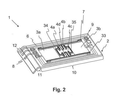
The MEMS printed circuit board unit 1 shown in Figure 2 comprises three
sections or partial areas, namely a main area 10, a kinking / bending area 11
and
a contact area 12. The main area 10 comprises the electrical contacts 9
located
on one side of the printed circuit board 2, of which only one is provided with
a
reference sign, for reasons of clarity. These are intended to electrically
connect
the MEMS printed circuit board unit 1 according to Figure 9 to a second
printed
circuit board unit 16.
The structure 3a, 3b of the MEMS printed circuit board unit 1 is at least
partially
cut free according to the embodiment shown in Figure 2 (the same applies to
the
embodiment shown in Figure 3). For this purpose, the printed circuit board 2
features at least one recess 7, 33, 34, 35 that is continuous ¨ that is,
extending
from the upper side to the lower side. By means of this, the structure 3a, 3b
is at
least partially cut free in its edge area. In the present case, the printed
circuit
CA 03000054 2018-03-27
14
board 2 comprises a first recess 7 and a second recess 33 that laterally cut
free
the structure 3a, 3b, the connecting elements 4a ¨ 4d and/or the fastening
area 5
with respect to the part of the printed circuit board 2 acting as a support
frame.
Furthermore, the printed circuit board 2 comprises a third and/or fourth
recess 34,
35. By means of this, the respective structure 3a, 3b is cut free with respect
to the
allocated connecting elements 4a ¨ 4d and/or the fastening area 5. The same
applies to the embodiment shown in Figures 3 and 4.
Thus, the structure 3a, 3b, the at least one flexible connecting element 4a ¨
4d
and the fastening area 5 are cut free from each other and from the support
frame
of the printed circuit board 2. The recesses 7, 33, 34, 35 enable a force-
reduced
deflection of the fastening area 5. Furthermore, this can be used to generate
a
larger lift. By contrast, the woven contact paths 6 are integrated in the PCB
2
completely; that is, from all sides.
The second partial area, which is configured as a kinking / bending area 11,
is
located between the contact area 12 and the main area 10. The third partial
area,
namely the contact area 12, features at least one external contact 8 for
electrically connecting the MEMS printed circuit board unit 1 to an external
device
(not shown in the figures). The kinking / bending area 11 is designed to be
more
elastic than the main area 10, such that preferably a kink of up to 900 is
possible.
As a result, the external contacts 8 can be arranged from the side on a
housing
according to the embodiment shown in Figure 9. In order to be able to ensure
sufficient flexibility of the kinking / bending area 11, exclusively woven
contact
paths 6 are located in this. The structure 3 does not extend into these.
Figures 3 and 4 show an additional embodiment of the MEMS printed circuit
board unit 1. In this case, the structure 3a, 3b, the connecting elements 4a ¨
4d
and/or the fastening area 5 are cut free from each other and/or from the
printed
circuit board frame, in particular by means of at least one of the recesses 7,
33,
34, 35. The printed circuit board 2 features electrical contacts 9 only on one
side,
the upper side in accordance with the depiction.
CA 03000054 2018-03-27
Figure 4 shows a sectional view of the MEMS printed circuit board unit 1
described above, which comprises the printed circuit board 2 and the multi-
layer
piezoelectric structure 3. According to Figure 4, the structure 3 features a
piezo
layer 13, a support layer 14 (in particular, a metallic support layer 14)
and/or at
least one electrode layer 15. According to the present embodiment, the support
layer 14 is formed as an electrode layer 15 and is electrically coupled
directly to
the piezo layer 13. The fastening area 5, in which a coupling element 21 can
be
fastened (compare, for example, Figure 6), is located at the center. The
support
layer 14 preferably extends at least partially into the anchor area 32.
Furthermore, the support layer 14 preferably extends over the entire area of
the
cantilever, the connecting elements 4a ¨ 4d and/or the fastening area 5. By
contrast, the piezo layer 13 is preferably limited to the area of the
cantilever.
Figures 5 and 6 show a first embodiment of a sound transducer assembly 20.
The sound transducer assembly 20 features a housing 30, which is formed from
a membrane frame 23 of a membrane module 17, the MEMS printed circuit board
unit 1 (which is formed, in particular, according to one of the two
embodiments
shown in Figure 1 or 3), a second printed circuit board unit 16 and/or a
housing
part 19.
In contrast to the MEMS printed circuit board unit 1, the second printed
circuit
board unit 16 is formed to be rigid, and not flexible. For this purpose, the
base
body of the second printed circuit board unit 16 is preferably formed from a
fiber
composite material. The second printed circuit board unit 16 comprises a gap
31.
This is formed to be continuous and extends from a first end side to an
opposite
second end side of the second printed circuit board unit 16. Accordingly, the
gap
31 comprises two opposing openings 25, 26. The housing part 19 is arranged in
the area of one of such two openings 26. Accordingly, the housing part 19
closes
off the gap 31 at one side, by which a cavity 24 is formed.
The flexible MEMS printed circuit board unit 1 is arranged at the other
opening 25
opposite the gap 31. For this purpose, the MEMS printed circuit board unit 1
is
attached to the front side of the rigid second printed circuit board unit 16.
Accordingly, the rigid second printed circuit board unit 16 forms a rigid
support
CA 03000054 2018-03-27
16
frame for the flexible MEMS printed circuit board unit 1, with respect to
which the
structure 3 can deflect the fastening area 5 together with the coupling
element 21
along the lifting axis.
As already mentioned above, the first MEMS printed circuit board unit 1 is
arranged at the first opening 25 of the gap 31 and the housing part 19 is
arranged
at the second opening 26. The housing part 19 closes the gap 31 on the side of
the second opening 26, such that the volume of the cavity 24 is defined by the
gap 31 and the partial hollow space formed by the housing part 19.
According to the embodiment shown in Figures 5 and 6, the MEMS printed circuit
board unit 1 is arranged between the membrane module 17 and the rigid second
printed circuit board unit 16. The second printed circuit board unit 16 is
connected
to the first MEMS printed circuit board unit 1 by means of electrical contacts
9.
According to the present embodiment, the external contacts 8 of the sound
transducer assembly 20 are arranged on the second printed circuit board unit
16,
in particular outside the cavity 24 and/or on its side turned away from the
MEMS
printed circuit board unit 16.
According to the present embodiment, at least one electronic component 18a,
18b is integrated in the second printed circuit board unit 16.
The membrane module 17 comprises, in addition to the membrane frame 23, the
membrane 22. This is accommodated in the membrane frame 23 in its edge area
in the z-direction or along the lifting axis in an oscillating manner. When
the
structure 3 is electrically excited, the coupling element 21, together with
the
membrane 22, begins to oscillate relative to the second printed circuit board
unit
16.
Figures 7, 9 and 10 show additional embodiments of the sound transducer
assembly 20, whereas each essentially addresses the differences with respect
to
the embodiment already shown and described in Figure 5. Thus, with the
following description, the additional embodiments for the same characteristics
use the same reference signs. Unless they are once again explained in detail,
CA 03000054 2018-03-27
17
their design and/or mode of action corresponds to the features already
described
above. The differences described below can be combined with the features of
the
respective preceding and following embodiments.
Figures 7 and 8 show an alternative sound transducer assembly 20, which is
formed essentially according to the embodiment described above. Thus, the
housing 30 is also formed herein by the membrane frame 23, the first MEMS
printed circuit board unit 1, the second printed circuit board unit 16 and the
housing part 19. However, according to the present embodiment, the second
printed circuit board unit 16 is arranged above the first MEMS printed circuit
board unit 1. Thus, the second printed circuit board unit is arranged between
the
first MEMS printed circuit board unit 1 and the membrane module 17. This
reduces the cavity 24 by the length of the gap 31. With this embodiment, the
external contacts are formed on the MEMS printed circuit board unit 1, namely
on
the side turned away from rigid printed circuit board unit 16. Thus, the
external
electrical contacts 8 are located on the lower side.
Figure 9 shows, in a sectional view, an additional embodiment of the sound
transducer assembly 20, which features the first MEMS printed circuit board
unit
1 described with reference to Figure 2. The second printed circuit board unit
16 is
located above the first MEMS printed circuit board unit 1 and thus between the
membrane module 17 and the first MEMS printed circuit board unit 1. The
housing 30 is formed from the membrane frame 23 and the second printed circuit
board unit 16 along with the housing part 19. The electrical components 18, 18
a,
such as an ASIC and/or a additional passive component, are integrated in the
second printed circuit board unit 16. The contact area 12 is located outside
the
sound transducer assembly 20 and can be moved in a variable manner by means
of the kinking / bending area 11.
Figure 10 shows a sectional view of the sound transducer assembly 20 according
to an additional embodiment. The sound transducer assembly 20 features a
plastic element 27, which essentially forms the housing part 19. Electrical
lines 28
are located in the plastic element 27. The electrical lines 28 extend
laterally
CA 03000054 2018-03-27
18
outward and serve as external contact for electrically connecting the sound
transducer assembly 20 with an external device (not shown in the figure).
Figure 11 shows a sectional view of the multi-layer piezoelectric structure 3
according to a first embodiment. The structure 3 comprises two electrode
layers
15 and one piezo layer 13 arranged between them. Furthermore, an insulation
layer 29 is arranged between the support layer 14 and the lower electrode
layer
15. The support layer 14 is electrically decoupled from the lower electrode
layer
15 by means of the insulating layer 29. The support layer 14 is preferably
made
of a metal, in particular copper. In addition, the support layer 14 preferably
features a thickness of between 2 to 50 pm.
Figure 12 shows a sectional view of the multi-layer piezoelectric structure 3
according to an additional embodiment. Here, the structure 3 comprises an
upper
electrode layer 15, a support layer 14 acting as an electrode layer and a
piezo
layer 13 arranged between the two. Thus, the support layer 14 is electrically
coupled to the piezo layer 13. The support layer 14 is preferably made of a
metal,
in particular copper. In addition, the support layer 14 preferably features a
thickness of between 2 to 50 pm.
The embodiments of the structure 3 shown in Figures 11 and 12 may feature at
least one additional piezoelectric layer in an embodiment that is not shown
here.
This is preferably also arranged between two electrode layers allocated to it.
Ac-
cordingly, the structure 3 would comprise two piezo layers 13. At this, one of
the
electrode layers 15 (in particular, of the four electrode layers 15) may be
formed
by the support layer 14. The support layer is preferably made of a metal, in
par-
ticular copper. If the structure features multiple piezoelectric layers, the
structure
can generate more force and bring about greater deflection. In this
connection, it
is also advantageous if the structure features more than two such piezo layers
13.
This invention is not limited to the illustrated and described embodiments.
Variations within the scope of the claims, just as the combination of
CA 03000054 2018-03-27
19
characteristics, are possible, even if they are illustrated and described in
different
embodiments.
CA 03000054 2018-03-27
List of Reference Skins
1 MEMS printed circuit board unit
2 Circuit board
3 Multi-layer piezoelectric structure
4 Flexible connecting element
5 Fastening area
6 Woven contact paths
7 First recess
8 External contact
9 Electrical contact
10 Main area
11 Kinking / bending area
12 Contact area
13 Piezo layer
14 Support layer
15 Electrode layer
16 Second printed circuit board unit
17 Membrane module
18 Electronic component
19 Housing part
20 Sound transducer assembly
21 Coupling element
22 Membrane
23 Membrane frame
24 Cavity
First opening of the gap
26 Second opening of the gap
27 Plastic element
28 Electrical lines
29 Insulation layer
Housing
31 Gap
CA 03000054 2018-03-27
21
32 Anchor area
33 Second recess
34 Third recess
35 Fourth recess