Note: Descriptions are shown in the official language in which they were submitted.
84236390
COMMUNICATIONS DEVICE WITH ANTENNA ELEMENT LAYOUT RELATIVE
TO CHAMFERED VERTEX OF MOUNTING PLANE
TECHNICAL FIELD
[0001] The present invention relates to the field of communications
technologies, and in
particular, to a communications device.
BACKGROUND
[0002] An omnidirectional antenna is a type of antenna commonly used in
an existing
mobile communications device, and the omnidirectional antenna is widely
applied to existing
networks. In recent years, mobile communication develops towards high-order
modulation,
broadband, and multiple-input multiple-output technology (MIMO). The multiple-
input
multiple-output technology (MIMO) is an extremely important development
direction. In the
multiple-input multiple-output technology, a transmit end and a receive end
use multiple
transmit antennas and multiple receive antennas, so that signals are
transmitted by using
multiple antennas of the transmit end and the receive end. Therefore, the
multiple-input
multiple-output technology can exponentially increase a system capacity and
improve spectral
efficiency without increasing a spectrum resource. In the MIMO technology, an
antenna
technology is crucial, especially to a mobile communications device
integrating an antenna.
The following requirements pose a quite big challenge to antenna design:
antenna
miniaturization, broadbandization (standing wave broadbandization and pattern
broadbandization), isolation between multiple antennas, and a correlation
between multiple
antennas.
[0003] Isolation between antennas and a correlation between antennas are
crucial
indicators for obtaining a high MIMO gain. A lower correlation between
antennas indicates
that a higher MIMO gain can be obtained. The isolation between antennas is an
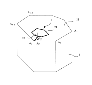
important
.. indicator for obtaining a low correlation between antennas. However,
because of a
miniaturization requirement, it is a quite big challenge to obtain maximum
isolation between
antennas in a module having a given size.
[0004] In addition, a power balance between multiple antennas is also an
extremely
CA 3000544 2019-07-29
84236390
important aspect. In the multiple-input multiple-output technology, an
excessively big power
difference between multiple paths usually compromises a MIMO gain. A small
tracking
difference between patterns of multiple antennas is required for achieving the
power balance,
and for the omnidirectional antenna, this means that a good roundness (or non-
roundness)
indicator needs to be achieved. In an existing radio transceiver module
integrating multiple
antennas, for a purpose of module miniaturization, antenna elements of a PIFA
or PILA type
are usually selected. For a pattern of a PIFA or PILA, it is usually difficult
to achieve a
roundness as an independent omnidirectional antenna supporting SISO. This
leads to a big
tracking difference between patterns of multiple antennas, and affects MIMO
performance to
an extent.
[0005] In an existing common omnidirectional antenna, such as a monopole
antenna or a
discone antenna with wider bandwidth, a feedpoint and a radiator of the
antenna are usually
placed in central positions of a ground, and the radiator of the antenna is
parallel with a
normal line direction of the ground. This perfect rotational symmetry in terms
of structure
ensures a quite small horizontal fluctuation of a pattern of the antenna, so
as to achieve an
effect of even coverage.
[0006] All existing structures are designed based on a symmetrical
structure. When a
multi-antenna array is designed by using antenna elements designed based on
the symmetrical
structure, symmetry of an antenna radiation structure is maintained, but
symmetry of the
ground cannot be satisfied. This asymmetry usually causes current asymmetry on
a carrier
surface, and further leads to pattern distortion. A part of design can be
maintained relatively
good in a narrowband range, but it is quite difficult to achieve relatively
wide bandwidth.
[00071 In addition, after an omnidirectional antenna element in the prior
art is integrated
on a carrier, a pattern of an antenna is extremely sensitive to a shape change
of the carrier. For
example, when the carrier is relatively thin (for example, 0.01 X,. where X is
a wavelength
corresponding to a minimum operating frequency of the antenna), a roundness of
the pattern
of the antenna can be 2.5 dB. However, because the radio transceiver module
includes
multiple parts, such as a circuit board, a heat sink, and a shield cover, a
thickness of a radio
transceiver module integrating the antenna is usually greater than 0.01 X.
Therefore, when the
antenna element in the prior art is integrated on such a module, the roundness
of the pattern of
the antenna may significantly deteriorate.
2
CA 3000544 2018-04-26
= ' 84236390
[0008]
A pattern of an antenna located on a corner of the carrier has poor roundness
performance because of deterioration of symmetry of a ground around the
antenna. As shown
in FIG. 1, FIG. 1 is a typical horizontal plane pattern of a broadband antenna
that has a
Patch-Slot-Pin (PSP) structure and that is mounted on a surface of a square
prism carrier. It
can be seen from FIG. 1 that depressions of different degrees exist in a
shadow area of the
figure, and the pattern has poor roundness performance.
SUMMARY
[0009]
The present invention provides a communications device, so as to improve
roundness performance of an antenna of the communications device and further
enhance an
antenna signal coverage effect.
[0010] According to a first aspect, a communications device is
provided, and the
communications device includes: a metal carrier, where the metal carrier has a
mounting plane,
and at least one mounting area is defined on the mounting plane; and
an antenna element disposed in each mounting area, where the antenna element
includes: a radiation structure and a feed structure connected to the
radiation structure, the
feed structure is fastened to the mounting plane, and a point at which the
feed structure is
connected to the mounting plane is a feedpoint; where
the mounting area is an area in which the mounting plane intersects a circle
centered at the feedpoint of the antenna element in the mounting area and
whose radius does
not exceed a specified radius;
when a boundary line of any of the mounting area includes a boundary line of
the
mounting plane, a distance from a feedpoint of an antenna element in the
mounting area to the
boundary line of the mounting area is less than or equal to a specified
distance; and/or when a
boundary line of the mounting area includes a vertex of the mounting plane, a
distance from
the feedpoint of the antenna element in the mounting area to the vertex is
less than or equal to
a specified distance.
[0011]
With reference to the first aspect, in a first possible implementation, the
specified
distance is 0.12
the specified radius is 0.25 24, and 24 is a wavelength corresponding to a
minimum operating frequency of the antenna element.
3
CA 3000544 2018-04-26
84236390
[0012] With reference to the first aspect or the first possible
implementation of the first
aspect, in a second possible implementation, a height of the antenna element
is not greater
than 0.25 Xi.
[0013] With reference to any one of the first aspect, the first possible
implementation of
the first aspect, or the second possible implementation of the first aspect,
in a third possible
implementation, the vertex has a structure of a chamfer, and the distance from
the feedpoint to
the vertex is a distance from the feedpoint to a point at which a connection
line between an
intersection of extension lines of two boundary lines of the chamfer and the
feedpoint
intersects the chamfer.
[0014] With reference to any one of the first aspect, the first possible
implementation of
the first aspect, the second possible implementation of the first aspect, or
the third possible
implementation of the first aspect, in a fourth possible implementation, the
metal carrier is a
ground of the antenna element, a metal housing of a wireless device, or a
circuit board or heat
sink of a wireless device.
[0015] With reference to any one of the first aspect, the first possible
implementation of
the first aspect, the second possible implementation of the first aspect, the
third possible
implementation of the first aspect, or the fourth possible implementation of
the first aspect, in
a fifth possible implementation, the feed structure is a feed probe.
[0016] With reference to the fifth possible implementation of the first
aspect, in a sixth
possible implementation, the feed probe is a column structure, or
the feed probe is a conductor sheet whose width gradually increases in a
direction
from the feedpoint to the radiation structure.
[0017] With reference to any one of the first aspect, the first possible
implementation of
the first aspect, the second possible implementation of the first aspect, the
third possible
implementation of the first aspect, the fourth possible implementation of the
first aspect, the
fifth possible implementation of the first aspect, or the sixth possible
implementation of the
first aspect, in a seventh possible implementation of the first aspect, the
radiation structure
includes at least one radiation patch.
[0018] With reference to the seventh possible implementation of the first
aspect, in an
eighth possible implementation, the radiation structure includes one radiation
patch, and the
radiation patch is an active radiation patch.
4
CA 3000544 2018-04-26
84236390
[0019] With reference to the seventh possible implementation of the first
aspect, in a ninth
possible implementation, the radiation structure includes two radiation
patches, the two
radiation patches are respectively a passive radiation patch and an active
radiation patch, the
active radiation patch is connected to the feed probe, the passive radiation
patch is connected
to a ground cable, and optionally, the active radiation patch and the passive
radiation patch are
connected by using at least one capacitance or inductance signal.
[0020] With reference to the ninth possible implementation of the first
aspect, in a tenth
possible implementation, the radiation structure further includes a dielectric
plate or plastic
support, the passive radiation patch and the active radiation patch are
disposed on the
dielectric plate or plastic support, or the dielectric plate or plastic
support is a flat plate or a
stepped plate, and when the dielectric plate or plastic support is a stepped
plate, the passive
radiation patch and the active radiation patch are respectively disposed on
different step
surfaces.
[0021] With reference to the tenth possible implementation of the first
aspect, in an
eleventh possible implementation, the dielectric plate or plastic support, the
active radiation
patch, and the passive radiation patch are an integrated printed circuit
substrate structure.
[0021a] Another aspect of the present disclosure relates to a communications
device,
comprising: a metal carrier, wherein the metal carrier has a mounting plane,
and at least one
mounting area is defined on the mounting plane; and an antenna element
disposed in each
mounting area, wherein the antenna element comprises: a radiation structure
and a feed
structure connected to the radiation structure, the feed structure is fastened
to the mounting
plane, and a point at which the feed structure is connected to the mounting
plane is a feedpoint;
wherein the mounting area is an area in which the mounting plane intersects a
circle centered
at the feedpoint of the antenna element in the mounting area and whose radius
does not
exceed a specified radius; when a boundary line of the mounting area comprises
a boundary
line of the mounting plane, a distance from the feedpoint of the antenna
element in the
mounting area to the boundary line of the mounting area is less than or equal
to a specified
distance; and/or when a boundary line of the mounting area comprises a vertex
of the
mounting plane, a distance from the feedpoint of the antenna element in the
mounting area to
the vertex is less than or equal to a specified distance, wherein the vertex
has a structure of a
chamfer, and the distance from the feedpoint to the vertex is a distance from
the feedpoint to a
5
CA 3000544 2019-07-29
84236390
point at which a connection line between an intersection of extension lines of
two boundary
lines of the chamfer and the feedpoint intersects the chamfer.
[0022] According to the communications device provided in the first
aspect, the metal
carrier is considered as a part of an antenna body for joint design. The
antenna element is
arranged in a specific corner position on the metal carrier. A feedpoint
position on the antenna
element is designed to obtain relatively good antenna roundness performance
and enhance an
antenna signal coverage effect.
BRIEF DESCRIPTION OF DRAWINGS
[0023] FIG. 1 is a typical horizontal plane pattern of a broadband
antenna that has a PSP
structure and that is mounted on a surface of a square prism carrier in the
prior art;
[0024] FIG. 2 is a schematic structural diagram of an antenna according
to an embodiment
of the present invention;
[0025] FIG 3 is a contour map of antenna roundnesses in different feed
positions on an
edge and a corner of one plane of a cuboid carrier;
[0026] FIG 4a to FIG 4f are schematic diagrams of a bottom surface of an
area occupied
5a
CA 3000544 2019-07-29
84236390
by a radiation structure according to embodiments of the present invention;
[0027] FIG 5 is a diagram of roundness comparison between an antenna
according to an
embodiment of the present invention and an antenna in the prior art;
[0028] FIG 6 is a schematic three-dimensional diagram of an antenna
according to
Embodiment 1 of the present invention;
[0029] FIG 7 is a top view of the antenna according to Embodiment 1 of
the present
invention;
[0030] FIG 8 is a side view of an antenna according to an embodiment of
the present
invention;
[0031] FIG. 9 is a roundness diagram of an antenna according to an
embodiment of the
present invention;
[0032] FIG 10 is a top view of an antenna according to Embodiment 2 of
the present
invention;
[0033] FIG. 11 is a side view of the antenna according to Embodiment 2 of
the present
invention;
[0034] FIG 12 is a roundness diagram of the antenna according to
Embodiment 2 of the
present invention;
[0035] FIG. 13 is a three-dimensional diagram of an antenna according to
Embodiment 3
of the present invention;
[0036] FIG 14 is a top view of the antenna according to Embodiment 3 of the
present
invention;
[0037] FIG 15 is a schematic diagram of structural parameters of the
antenna according to
Embodiment 3 of the present invention;
[0038] FIG 16 is a side view of the antenna according to Embodiment 3 of
the present
invention; and
[0039] FIG 17 is a roundness diagram of the antenna according to
Embodiment 3 of the
present invention.
[0040] Reference numerals:
1: Metal carrier; 11: Mounting plane; 2: Antenna element;
21: Radiation structure; 211: Active radiation patch; 212: Passive radiation
patch;
213: Dielectric plate or plastic support; 22: Feed structure; and 23: Ground
cable
6
CA 3000544 2018-04-26
= 84236390
DESCRIPTION OF EMBODIMENTS
[0041] The following describes the specific embodiments of the
present invention in detail
with reference to accompanying drawings. It should be understood that the
specific
implementations described herein are merely used to explain the present
invention but are not
intended to limit the present invention.
[0042] As shown in FIG 2 and FIG. 6, FIG 2 and FIG. 6 show structures
of
communications devices with different structures provided in the embodiments
of the present
invention.
[0043] An embodiment of the present invention provides a
communications device. The
communications device includes a metal carrier 1, where the metal carrier 1
has a mounting
plane 11, and at least one mounting area is defined on the mounting plane; and
an antenna element 2 disposed in each mounting area, where each antenna
element
2 includes: a radiation structure 21 and a feed structure 22 connected to the
radiation structure
21, the feed structure 22 is fastened to the mounting plane 11, and a point at
which the feed
structure 22 is connected to the mounting plane 11 is a feedpoint; where
the mounting area is an area in which the mounting plane intersects a circle
centered at the feedpoint of the antenna element in the mounting area and
whose radius does
not exceed a specified radius;
when a boundary line of any of the mounting area includes a boundary line of
the
mounting plane 11, a distance from a feedpoint of an antenna element 2 in the
mounting area
to the boundary line of the mounting area is less than or equal to a specified
distance, and/or
when the boundary line of the mounting area includes a vertex of the mounting
plane, a
distance from the feedpoint of the antenna element in the mounting area to the
vertex is less
than or equal to a specified distance.
[0044] In the foregoing embodiment, the metal carrier 1 is considered as a
part of an
antenna body for joint design. The antenna element 2 is arranged in a specific
corner position
on the metal carrier 1. A feed position on the antenna element 2 is designed
to obtain
relatively good antenna roundness performance and enhance an antenna signal
coverage
effect.
[0045] Optionally, the antenna element is fastened to the metal carrier by
using a screw or
7
CA 3000544 2018-04-26
84236390
glue. For a specific mounting or fastening manner, refer to the prior art. No
limitation is
imposed herein.
[0046] Specifically, most energy of an electronically small antenna (the
electronically
small antenna is usually an antenna whose maximum size is less than 0.25 times
a wavelength)
integrated on a metal carrier is radiated out by the carrier. The antenna can
be considered as a
coupler, and its function is coupling electromagnetic energy onto the carrier,
so that the
electromagnetic energy is radiated out by the carrier. In a conventional idea,
to ensure
symmetry of a pattern of the antenna, a ground structure (or carrier
structure) of the antenna is
designed as a symmetrical structure, and the antenna is placed in a symmetric
center.
[0047] It can be found from research that the carrier of the antenna
usually has some fixed
characteristic modes, these characteristic modes are theoretically orthogonal,
and an overall
pattern of the antenna may be decomposed into a linear combination of these
characteristic
modes. When the antenna is placed in different positions, combinations of
different
characteristic modes are excited, and different patterns are further obtained.
In the present
invention, based on this principle, the antenna is excited in an edge and/or a
corner position of
the carrier, and a pattern roundness is calculated, so as to obtain a
relatively good roundness.
For an electrically small antenna mounted on a metal carrier, energy is
radiated out by an
antenna body and the carrier. In some cases, carrier radiation accounts for
80% of total
radiated energy. Therefore, not merely the antenna is exited. In some cases,
the antenna is
.. understood as a coupler that couples energy onto the carrier, so that the
energy is radiated out
by the carrier.
[0048] For example, FIG 3 is a gradient map (similar to a geographical
contour map) of
pattern roundnesses in different antenna excitation positions around different
vertexes AO on
one plane of a cuboid carrier. It can be clearly seen from FIG. 3 that an area
(marked as 4, 5,
and 6 in the figure) with an optimal roundness exists within a specific
distance from a vertex
AO. An antenna provided in the present invention is designed based on the
foregoing principle.
Disposing position of an antenna element on a corner of the carrier is
obtained, and the
antenna is disposed in a vertex position of the carrier in the foregoing
disposing manner, so
that the antenna element in the vertex position of the carrier has relatively
good roundness
performance. In addition, when multiple antenna elements are disposed on the
carrier, a
distance between the antenna elements increases, and this leads to high
isolation between the
8
CA 3000544 2018-04-26
= 84236390
antenna elements.
[0049] In addition, when a feedpoint of the antenna is placed on a comer,
a real part of
radiation impedance of the antenna increases, and this is extremely beneficial
to antenna
miniaturization. A size of the antenna designed by using this method is
usually smaller than a
size of an antenna with same bandwidth in the prior art. Therefore, when more
antennas are
placed in a same area, a distance between the antennas can be longer, and
isolation between
the antennas can be effectively improved.
[0050] To facilitate understanding of the antenna provided in this
embodiment of the
present invention, the following describes a structure of the antenna in
detail with reference to
a specific embodiment.
[0051] Specifically, the communications device provided in this
embodiment may be a
radio frequency module, such as an indoor remote radio unit RRU (remote radio
unit), a base
station, or another communications device equipped with an antenna.
Optionally, in the
communications device, an antenna and another module are integrated. The
integration
includes sharing a cover.
[0052] In this embodiment, a monopole antenna is used as an example for
description.
First, for several distances in the antenna provided in this embodiment, the
distance from the
feedpoint to the vertex or an edge (the boundary line of the mounting plane)
of the mounting
plane 11 is denoted as Rc, the radius of the circle drawn with the feedpoint
as the center is
denoted as RANT, and the height of the antenna element is denoted as H.
[0053] In this embodiment, as a specific embodiment, the metal carrier
may be a right
prism carrier, and the right prism carrier is a column structure with a top
surface perpendicular
to a side surface.
[0054] In addition, when each antenna element is specifically disposed,
the antenna
element may have a ground cable or may not have a ground cable. In this
embodiment, the
antenna element having a ground cable is used as an example for description.
[0055] When the antenna element 2 is specifically disposed, the following
conditions may
be met: When a boundary line of a bottom surface of an area occupied by any
radiation
structure 21 includes a boundary line of the mounting plane 11, a distance
from the feedpoint
to the boundary line of the mounting area is less than or equal to the
specified distance, and/or
when a boundary line of the bottom surface includes a vertex of the mounting
plane 11, a
9
CA 3000544 2018-04-26
' 84236390
distance from the feedpoint to the vertex is less than or equal to the
specified distance. In
addition, in specific disposing, a height of an antenna is a vertical distance
from the radiation
structure 21 to the mounting plane 11. Optionally, when the radiation
structure 21 is
specifically disposed, the height of the antenna is not greater than the set
height in a specific
application scenario. In an example, the specified distance is 0.12 the
specified radius is
0.25 and
the set height is 0.25 i, where X1 is a wavelength corresponding to a minimum
operating frequency of the antenna. In this way, an optimal roundness value is
obtained for the
antenna.
[0056] In
this embodiment, different structures may be selected for the metal carrier 1
and
the antenna. The metal carrier 1 may be a ground of the antenna, a metal
housing of a wireless
device, a circuit board, shield cover, or heat sink of a wireless device, or
another structure.
The metal carrier 1 may be in different shapes such as a polygonal column and
a cylinder. One
plane of the metal carrier 1 is the mounting plane 11 of the antenna. The
mounting plane 11
may be in different shapes such as a polygon and a circle. When the metal
carrier 1 is a
polygonal column or a cylinder, the mounting plane 11 is correspondingly an
end face of the
metal carrier 1. In addition, when the metal carrier 1 is a polygonal column,
the vertex of the
mounting plane 11 has a structure of a chamfer, and the chamfer is a round
angle structure or
an oblique angle structure. In this case, the distance Rc from the feedpoint
to the vertex is a
distance from the feedpoint to a position of a point at which a connection
line between an
intersection of extension lines of two boundary lines of the chamfer and the
feedpoint
intersects the chamfer.
[0057] To
facilitate understanding of Rc, refer to FIG. 4a to FIG. 4f. FIG. 4a to FIG.
4f
show shapes of the bottom surface (mounting area) of the area occupied by the
radiation
structure 21 and specific distances Rc when the mounting plane 11 arc in
different shapes.
Referring first to FIG. 4a, the mounting plane 11 is polygonal, the vertex is
Ai, two sides are
respectively A,_IA, and A,Ai+i, and the feedpoint is F. In this case, the
distance Rc is a length
of FAõ and the mounting area is BA,¨AC¨CB. As shown in FIG 4b, the mounting
plane 11 is
circular. F is the feedpoint, Rc is a minimum distance from the feedpoint to
an arc of the
boundary line of the mounting plane 11, and the mounting area is CB¨BC. As
shown in FIG
4c, the mounting plane 11 is polygonal, F is the feedpoint, Rc is a vertical
distance from the
CA 3000544 2018-04-26
= ' 84236390
feedpoint to the boundary line BC of the mounting plane 11, a perpendicular
foot is Aõ and
the mounting area is BC¨CB. When the antenna is placed on a straight edge, C
(CD is a
degree of an interior angle of a corner of the mounting plane 11) is equal to
180 , and this is a
special case. As shown in FIG 4d, the special case in which C is equal to 180
is equivalent
to a case in which the antenna element 2 is placed on an edge. As shown in
FIG. 4e, a vertex
shown in FIG. 4e has a round chamfer. Specifically, the mounting plane 11 is
polygonal, the
vertex is A,, two sides are respectively A,_,A, and A,A,,i, the vertex A, is
an intersection of
extension lines of the two sides, and the feedpoint is F. In this case, the
distance Rc is a length
of FA,, and the mounting area is BA,¨A,C¨CB. As shown in FIG 4f, a vertex
shown in FIG 4f
has an oblique chamfer. Specifically, the mounting plane 11 is polygonal, the
vertex is Aõ two
sides are respectively A,A, and A1A0_1, the vertex A, is an intersection of
extension lines of
the two sides, and the feedpoint is F. In this case, the distance Rc is a
length of FA,, and the
mounting area is BA,¨AiC¨CB.
[0058] An antenna element 2 provided in this embodiment includes a
radiation structure
21, a feed structure 22, and a ground cable 23. The feed structure 22 may be a
feed probe. In
specific disposing, the feed probe may be designed in different shapes.
Optionally, the feed
probe is a column structure, or the feed probe is a conductor sheet whose
width gradually
increases in a direction from a feedpoint to the radiation structure 21. In
actual production, the
feed probe may be designed in the foregoing shapes according to different
requirements. It
should be understood that the foregoing two structures are examples of
specific structures and
do not limit a structure of the feed probe. The feed probe may be designed,
according to a
requirement, in any other structural shape meeting the requirement.
[0059] Referring to FIG 6 and FIG. 13, the radiation structure 21 may
include at least one
radiation patch. When the radiation structure 21 includes one radiation patch,
the radiation
patch is an active radiation patch 211. When multiple radiation patches are
used, the radiation
patches may be an active radiation patch 211 and a passive radiation patch 212
(the active
radiation patch 211 and the passive radiation patch 212 are structures that
are structurally
distinguished from each other, the active radiation patch is a portion
structurally connected
directly to a radio frequency transmission line, and the passive radiation
patch 212 is a portion
that is structurally spaced a distance apart from the active radiation patch
211 and is not
11
CA 3000544 2018-04-26
= 84236390
directly connected to the radio frequency transmission line). For example, the
radiation
structure 21 includes two radiation patches, the two radiation patches are
respectively the
passive radiation patch 212 and the active radiation patch 211, the active
radiation patch 211 is
connected to the feed probe, and the passive radiation patch 212 is connected
to the ground
cable 23. Optionally, the active radiation patch 211 and the passive radiation
patch 212 are
connected by using at least one capacitance or inductance signal. When
multiple radiation
patches are used, the radiation structure 21 may further include a dielectric
plate or plastic
support 213, and the passive radiation patch 212 and the active radiation
patch 211 are
disposed on the dielectric plate or plastic support 213. Therefore, an
integrated structure is
formed for the radiation structure 21. In specific design, the dielectric
plate or plastic support
213 may be a flat plate or a stepped plate. When the dielectric plate or
plastic support 213 is a
stepped plate, the passive radiation patch 212 and the active radiation patch
211 are
respectively disposed on different step surfaces. In addition, the radiation
patches and the
dielectric plate or plastic support 213 may be designed to be a split type or
an integrated type.
When the split type is used, the dielectric plate or plastic support 213 may
be a plastic plate.
When the integrated type is used, the dielectric plate or plastic support 213,
the active
radiation patch 211, and the passive radiation patch 212 are an integrated
printed circuit
substrate structure. This facilitates design and production of the radiation
structure 21. It can
be understood that the foregoing active radiation patch may also be designed
in a stepped
shape, and details are not described herein.
100601 In addition, in specific design, a radiation patch may be in
different shapes, for
example, a polygonal shape or a fan shape. When the radiation patch is in a
polygonal shape,
the radiation patch may be in a rectangular shape, a pentagonal shape, or a
different shape.
[0061] In this embodiment, optionally, the radiation structure 21 used in
the antenna is an
asymmetric structure relative to the feedpoint. When the antenna is arranged
on a corner of the
mounting plane 11, Rc can meet a requirement. Specifically, the requirement is
that Rc is less
than a specified distance, the specified distance is 0.12 2, and ki is a
wavelength
corresponding to a minimum operating frequency of the antenna. When the
feedpoint of the
antenna is placed in a position close to the corner, the antenna can maintain
good roundness
performance. When the distance Rc from the feedpoint to the vertex is less
than 0.12 24, a
roundness of the antenna is optimal. As shown in FIG. 5, FIG. 5 shows
comparison between a
12
CA 3000544 2018-04-26
= 84236390
roundness value of the antenna provided in this embodiment and that of an
antenna in the
prior art. A horizontal coordinate indicates a frequency in a unit of GHz, and
a vertical
coordinate indicates a roundness in a unit of dB. It can be seen from FIG 5
that the roundness
value of the antenna provided in this embodiment is much better than that of
the antenna in
the prior art. Optionally, the radiation structure 21 used in the antenna may
be a symmetrical
structure relative to the feedpoint, and details are not described herein.
[0062] The following describes structures of the antenna provided in the
embodiments of
thc present invention in detail with reference to specific accompanying
drawings. In the
following specific embodiments, different values of the distance Re from the
feedpoint to the
vertex or boundary line of the mounting surface are given for emulation, and
specific
structural parameters used during mounting of the antenna element are given.
The structural
parameters may be designed according to an actual situation. The following
embodiments are
merely emulation descriptions by using a specific structure of a specific
antenna as an
example.
Embodiment 1
[0063] Referring to FIG. 6 to FIG 9, FIG. 6 is a schematic three-
dimensional diagram of
an antenna provided in this embodiment, FIG 7 is a top view of the antenna
provided in this
embodiment, FIG 8 is a side view of the antenna provided in this embodiment,
and FIG 9 is a
roundness diagram of the antenna provided in this embodiment.
[0064] As shown in FIG 6, the antenna in this embodiment of the present
invention
includes one cuboid metal carrier 1 and one antenna element 2 that is designed
according to
the foregoing principle. The antenna element 2 is mounted on a metal plane of
the metal
carrier 1, and the metal plane is a mounting surface 11. The metal carrier 1
may be a structure
in different shapes, for example, a polygonal column or a cylinder. In this
embodiment. the
metal carrier 1 is a cuboid, the antenna element 2 includes a feed probe, an
active radiation
patch 211, and one or more ground cables 23, and the active radiation patch
211 is in any
shape. The active radiation patch 211 and the metal plane (the mounting
surface 11) are
connected by using the ground cable 23.
[0065] When the radiation patch is in a square shape, a good match and a
good pattern
13
CA 3000544 2018-04-26
84236390
may be obtained in an operating frequency band by adjusting a size of the
antenna.
[0066] As shown in Table 1, FIG. 7, and FIG 8, Table 1 lists key
structural parameters in
Embodiment 1 (ki is a wavelength corresponding to a minimum operating
frequency).
Structural Parameter Structural Parameter Description .. Electrical length
(Xi)
a Distances from a side PO-P1 of a square 0.046
patch P0-P1-P2-P3 to a side AO-A 1 of a
mounting plane and from a side PO-P3
of the square patch to a side AO-A3 of
the mounting plane in an X-Y plane
Distances from a feedpoint F to the side 0.051
AO-A 1 and to the side AO-A3 of the
mounting plane in the X-Y plane
Distances from a shorting pin to the side 0.090
AO-A 1 and to the side AO-A3 of the
mounting plane in the X-Y plane
Ws Width of the shorting pin 0.015
Side length of the square patch 0.138
P0-P1-P2-P3
Distance from the square patch 0.057
P0-P1-P2-P3 to the mounting plane
AO-A1-A2-A3 in a Z direction
Rc Distance from the feedpoint F to a 0.073
vertex AO of the carrier plane in the X-Y
plane
[0067] Referring to FIG 9, FIG 9 shows a pattern roundness of the antenna
element that is
disposed according to the structural parameters in Table 1 and operates at
frequencies in
Table 2.
[0068] Table 2 is as follows:
14
CA 3000544 2018-04-26
84236390
Frequency Roundness (Theta = 80 deg, where theta indicates a theta
axis of a
GHz spherical coordinate system, and deg is a unit, that is,
degree)
dB
1.71 1.8
1.76 1.8
1.81 2.1
1.86 2.5
1.88 2.8
Embodiment 2
[0069] Referring to FIG 10 to FIG. 12, FIG 10 is a top view of an antenna
provided in this
embodiment, FIG. 11 is a side view of the antenna provided in this embodiment,
and FIG 12
is a roundness diagram of the antenna provided in this embodiment.
[0070] Referring first to FIG. 10 and FIG. 11, the antenna in this
embodiment includes one
euboid metal carrier 1 and one antenna element 2 that is designed according to
the foregoing
principle. The antenna element 2 is mounted on a metal plane of the metal
carrier 1. Further,
the metal carrier 1 is a cuboid, and the antenna element 2 includes a feed
probe, an active
radiation patch 211, and one or more ground cables 23. The active radiation
patch is in any
shape, for example, the patch is designed in a fan shape in this embodiment.
[0071] When the patch is in a circular shape, a good match and a good
pattern may be
obtained in an operating frequency band by adjusting a size of the antenna.
[0072] Referring to Table 3, Table 3 lists key structural parameters in
Embodiment 2 (X1 is
a wavelength corresponding to a minimum operating frequency.)
[0073] Table 3 is as follows:
CA 3000544 2018-04-26
= = 84236390
Structural Parameter Structural Parameter Description .. Electrical
Length (34)
a Distances from a feedpoint center F to 0.0456
a side AO-Al and to a side AO-A3 of
the mounting plane in an X-Y plane
R1 Radius of the feed probe
0.0057
R2 Distance from the feedpoint center F 0.0684
to a shorting pin center S
R3 Radius of the radiation patch 0.16188
Ws Width of the shorting pin
0.01539
Re Distance from the feedpoint center F 0.064488138
to a vertex AO of the mounting plane
in the X-Y plane
Distance from the radiation patch to a 0.057
carrier plane
[0074] Referring to FIG. 12, FIG 12 shows a pattern roundness of the
antenna element 2
that is disposed according to the structural parameters in Table 3 and
operates at powers in
Table 4.
[0075] Table 4 is as follows:
Frequency Roundness (Theta = 80 deg)
CHz dB
1.71 1.6
1.76 1.6
1.81 1.8
1.86 2.3
1.88 2.5
16
CA 3000544 2018-04-26
84236390
Embodiment 3
[0076] Referring to FIG. 13 to FIG 17, FIG 13 is a three-dimensional
diagram of an
antenna provided in this embodiment, FIG. 14 is a top view of the antenna
provided in this
embodiment, FIG. 15 is a schematic diagram of structural parameters of the
antenna provided
in this embodiment, FIG 16 is a side view of the antenna provided in this
embodiment, and
FIG. 17 is a roundness diagram of the antenna provided in this embodiment.
[0077] As shown in FIG. 13, the antenna in this embodiment includes one
cuboid metal
carrier 1 and one antenna element 2 that is designed according to the
foregoing principle. The
antenna element 2 is mounted on a metal plane of the metal carrier 1. Further,
the metal carrier
1 is a cuboid, and the antenna element 2 includes a feed probe, one active
radiation patch 211,
and one passive radiation patch 212. Further, the passive radiation patch 212
and a ground
plane are connected by using one or more ground cables 23. The radiation
patches are in any
shape, for example, a square shape or a fan shape. The fan shape is used as an
example in this
embodiment.
[0078] Further, the active radiation patch 211 and the passive radiation
patch 212 are
supported by using a plastic plate, or the active radiation patch 211, the
passive radiation patch
212, and a dielectric plate or plastic support 213 are manufactured by using
one microstrip
board.
[0079] Standing wave bandwidth (VSWR < 2.5, where VSWR < 2.5 is a method
for
calculating the standing wave bandwidth, and indicates bandwidth meeting a
condition that
VSWR < 2.5) exceeding 45% may be achieved by adjusting the structural
parameters of the
antenna. In addition, a pattern roundness of the antenna maintains good
performance in the
bandwidth.
[0080] Specifically, referring to FIG 15, FIG 16, and Table 5, Table 5
lists specific values
of the structural parameters shown in FIG 15. Table 5 is as follows:
17
CA 3000544 2018-04-26
84236390
Structural Parameter Structural Parameter Description Value
Distance from a fan radiation patch to a 0.057 Xi
mounting plane of the carrier
Distances from a feedpoint F to a side 0.046 XI
AO-AI and to a side AO-A3 of the mounting
plane of the carrier in an X-Y plane
R1 Radius of the feed probe 0.011 A.1
R2 Radius of the active radiation patch that is a 0.05
Ai
fan centered at F
R3 Inner radius of the passive radiation patch 0.074 ki
that is a quarter of a circle centered at F
R4 Radius of a ground lug that is an arc 0.11 Xi
centered at F
R5 Outer radius of the passive radiation patch 0.1539
Xi
that is a quarter of a circle centered at F
Re Distance from the feedpoint F to a vertex 0.071 Xi
AO of a carrier plane in the X-Y plane
P Degree of an open angle of the ground lug 15.5 deg
that is an arc centered at F
[0081] In addition, F and S in the figure respectively indicate the
feedpoint F (Feeding)
and a ground point S (Shorting).
[0082] Referring to FIG. 17 and Table 6, FIG. 17 is a roundness diagram of
the antenna
provided in this embodiment, where the antenna is disposed according to the
structural
parameters in Table 5 and operates at frequencies in Table 6. Table 6 is as
follows:
18
CA 3000544 2018-04-26
" 84236390
Frequency Roundness (Theta = 80 deg)
CiHz dB
1.7 5
1.9 3
2.1 2.2
2.3 2
2.5 2.4
2.7 3
[0083] In addition, F and S in the figure respectively indicate the
feedpoint F (Feeding)
and a ground point S (Shorting).
[0084] It can be learned from the detailed descriptions in Embodiment 1,
Embodiment 2,
and Embodiment 3 that, in the antennas provided in the embodiments, a
feedpoint position of
the antenna element that is disposed on a corner of the carrier is arranged,
so that the antenna
element located in a vertex position of the carrier has relatively good
roundness performance.
In addition, when multiple antenna elements are disposed on the carrier, a
distance between
the antenna elements increases, so as to achieve high isolation between the
antenna elements.
[0085] Obviously, a person skilled in the art can make various
modifications and
variations to the present invention without departing from the scope of the
present invention.
The present invention is intended to cover these modifications and variations
provided that
they fall within the scope of protection defined by the following claims and
their equivalent
.. technologies.
19
CA 3000544 2018-04-26