Note: Descriptions are shown in the official language in which they were submitted.
CA 03000877 2018-04-04
Description
Electronic Circuit Breaker
The invention relates to an electronic circuit breaker having a control unit
and having a
controllable semiconductor switch connected in a current path between a
voltage input
and a load output. It additionally concerns a method for controlling an
electronic circuit
breaker of this nature.
An electronic circuit breaker of this type is described in DE 203 02 275 U1,
for example.
The electronic circuit breaker has a semiconductor switch in the form of a
MOSFET
(Metal Oxide Semiconductor Field Effect Transistor) that is connected in a
current path
between an operating voltage terminal and a load terminal. In order to achieve
reliable
current limiting in a DC network, a measured value sensed by a current sensor
in the
current path is fed to a comparator input of a control system. When an
activation signal
is present and a measured value falls below a reference value, the control
system
drives the semiconductor switch on, whereas in the case of a measured value
exceeding the reference value, the control system drives the power transistor
off and
limits the current flowing through it to the reference value.
Known from EP 1 186 086 B1 is a power distribution system in the low voltage
range, in
particular in the 24V DC range, having a number of circuits, each with an
electronic
circuit breaker as short circuit protection and/or overload protection. The
circuits are
supplied collectively by means of a clocked power supply. In the event of an
overload,
when an adjustable current threshold is exceeded, for example at 1.1 times the
nominal
current (IN), a blocking of the electronic circuit breaker takes place after a
delay period
has elapsed, whereas in the event of a short circuit, current limiting takes
place first,
and then after another current threshold is exceeded (e.g., 2 x IN) a blocking
of the
circuit breaker takes place after a specific turn-off time has elapsed.
2
Known from EP 1 150 410 A2 is an electronic circuit breaker, driven by means
of a
microprocessor via a trigger circuit, that disconnects the power supply to a
load with a
time delay. A partial disconnection of the circuit breaker takes place
beforehand or
simultaneously.
A partial disconnection of an electronic circuit breaker having multiple
circuit blocks,
each of which has an electronic switch in the form of a MOSFET and a
comparator
controlling the latter through a common microprocessor, is also known from
EP 1 294 069 B1. In the event of an overcurrent, the power supply to the load
is
disconnected after a time delay that follows a partial disabling of the at
least one switch.
For switching capacitive loads, in particular, and/or for protecting them from
overcurrent
and short-circuits, the semiconductor switch of the electronic circuit breaker
is used as a
constant-current source for charging the capacitance. The semiconductor
switch, and in
particular a MOSFET used here, must be capable of handling the power
dissipation
resulting from the inrush current during the switching or during the course of
charging
the capacitance. As a result of this situation, electronic circuit breakers,
especially those
with active current limiting, are usually designed with an oversize
semiconductor switch
(MOSFET) in order to adequately take this power dissipation into account.
However,
such dimensioning of the employed semiconductor switch entails an increased
cost and
a correspondingly large space requirement within the circuit of the electronic
circuit
breaker.
The invention has the object of specifying an electronic circuit breaker that
operates as
effectively as possible while avoiding the said disadvantages, wherein it is
desirable to
avoid an oversize semiconductor switch and the costly driving thereof. Also to
be
specified is a suitable method for controlling (driving) such an electronic
circuit breaker,
in particular even during a switch-on process of a load.
Date Recue/Date Received 2022-03-11
3
According to an aspect of the present invention, there is provided an
electronic circuit
breaker having a control unit and having a controllable semiconductor switch
connected
in a current path between a voltage input and a load output, characterized in
that the
semiconductor switch is integrated into a voltage-controlled current source
circuit, the
output current of which, when a load is connected, is set by means of the
control unit
such that the power of the semiconductor switch is less than or equal to a
maximum
power value, wherein the control unit sends a setpoint value to the voltage-
controlled
current source circuit, and receives from it a difference value that is
produced from a
deviation of an actual value representing the output current from the setpoint
value, and
is fed to the semiconductor switch as a control signal for driving the same.
According to another aspect of the present invention, there is provided the
electronic
circuit breaker as described herein, characterized in that the output voltage
of the
voltage-controlled current source circuit is fed to the control unit, which
determines the
power of the semiconductor switch, preferably from the output voltage and the
setpoint
value, and sets the maximum power value as a function of the output voltage.
According to another aspect of the present invention, there is provided the
electronic
circuit breaker as described herein, characterized in that the controllable
semiconductor
switch is driven within the voltage-controlled current source circuit such
that the output
current is limited in the event of an overload or short circuit, taking into
account the
maximum power value.
According to another aspect of the present invention, there is provided the
electronic
circuit breaker as described herein, characterized in that the control unit,
in the event of
an overload or short circuit, sets the setpoint value of the output current to
a
predefinable or predefined minimum value and increases it to a nominal value
if the
output voltage rises over time.
Date Recue/Date Received 2022-03-11
3a
According to another aspect of the present invention, there is provided the
electronic
circuit breaker as described herein, characterized in that the control unit
raises the
setpoint value of the output current stepwise as a function of the output
voltage.
According to another aspect of the present invention, there is provided the
electronic
circuit breaker as described herein, characterized in that the voltage-
controlled current
source circuit has an operational amplifier to whose input side are fed the
actual value
and the setpoint value of the output current, and the output side of which is
connected
to an input of the control unit and to the control side of the semiconductor
switch.
According to another aspect of the present invention, there is provided a
method for
controlling an electronic circuit breaker having a controllable semiconductor
switch
integrated into a voltage-controlled current source circuit,
- in which the output current of the current source circuit is sensed as an
actual value
and this value is compared with a setpoint value, producing a difference value
that
serves as a control signal for driving the semiconductor switch, and
- in which the setpoint value of the output current of the current source
circuit is set such
that the power of the semiconductor switch is always less than or equal to a
maximum
power value.
According to another aspect of the present invention, there is provided the
method as
described herein, characterized in that the output current is limited to a
current value if
the difference value of the output current produced from the actual value and
the
setpoint value reaches or exceeds a threshold value.
According to another aspect of the present invention, there is provided the
method as
described herein, characterized in that the output voltage of the current
source circuit is
Date Recue/Date Received 2022-03-11
3b
sensed, and the setpoint value of the output current is set as a function of
the output
voltage.
According to another aspect of the present invention, there is provided the
method as
described herein, characterized in that, in the event of an overload or short
circuit, the
setpoint value of the output current is set to a value and only increased
subsequently as
a function of the output voltage, in particular stepwise, if the output
voltage rises over
the course of time.
According to another aspect of the present invention, there is provided an
electronic
circuit breaker comprising:
a control unit; and
a controllable semiconductor switch connected in a current path between a
voltage
input and a load output, the semiconductor switch being integrated into a
voltage-
controlled current source circuit, an output current of which, when a load is
connected,
is set via the control unit such that a power of the semiconductor switch is
less than or
equal to a maximum power value,
wherein the control unit sends a setpoint value to the voltage-controlled
current source
circuit, and receives from the voltage-controlled current source circuit a
difference value
that is produced from a deviation of an actual value representing the output
current from
the setpoint value, and is fed to the semiconductor switch as a control signal
for driving
the same; and
wherein the control unit, in the event of an overload or short circuit, sets
the setpoint
value of the output current to a predefinable or predefined minimum value, and
the
predefinable or predefined minimum value increases to a nominal value when the
output voltage rises over time.
Date Recue/Date Received 2022-03-11
3c
According to another aspect of the present invention, there is provided a
method for
controlling an electronic circuit breaker having a controllable semiconductor
switch
integrated into a voltage-controlled current source circuit, the method
comprising:
sensing an output current of the current source circuit as an actual value and
this value
is compared with a setpoint value;
producing a difference value that serves as a control signal for driving the
semiconductor switch; and
setting the setpoint value of the output current of the current source circuit
such that the
power of the semiconductor switch is always less than or equal to a maximum
power
value,
wherein a control unit of the electronic circuit breaker, in the event of an
overload or
short circuit, sets the setpoint value of the output current to a predefinable
or predefined
minimum value, and the predefinable or predefined minimum value increases to a
nominal value when the output voltage rises over time.
According to the invention, the controllable semiconductor switch is wired to
form a
voltage-controlled current source, which is to say that it is integrated into
a
corresponding voltage-controlled current source circuit. The output current
thereof,
when a load is connected, is set by means of a control unit such that the
power of the
semiconductor switch is always less than or equal to a maximum power value.
The
control unit sends a setpoint value for the output current to the voltage-
controlled
current source circuit, and receives from it a difference value produced from
a deviation
of the output current from the setpoint value. The difference value serves to
drive the
semiconductor switch and is fed to it on the control side as a control signal
(control
voltage).
Date Recue/Date Received 2022-03-11
3d
To this end, a voltage of the voltage-controlled current source circuit
representing the
output current, as the actual value, and the circuit's output voltage, are
appropriately
supplied to the control unit. If the difference value produced in or by the
voltage-
controlled current source circuit deviates from a threshold value in the event
of an
overload or short circuit or during a switch-on to a capacitive load, this
state is detected
by the control unit on the basis of the difference value, and preferably a
current limiting
takes place initially. In addition, the control unit sets the setpoint value
of the output
current such that the maximum power value of the semiconductor switch is not
exceeded, which is to say the switch always operates within its safe operating
area
(safe operation area), taking its maximum power dissipation into account.
In an advantageous embodiment, the control unit of the electronic circuit
breaker sets
the setpoint value of the output current in the event of an overload or short
circuit, and
thus also during a switch-on to a capacitive load, such that this setpoint
value only rises
in the event of an output voltage that likewise rises over time, taking the
maximum
power value of the semiconductor switch into account and starting from a
minimum
value. The specification of the setpoint value by the control unit of the
electronic circuit
Date Recue/Date Received 2022-03-11
CA 03000877 2018-04-04
=
4
breaker is suitably carried out here in discrete steps, so that the output
current (load
current) rises stepwise. During the phases or steps of constant output
current, the
control unit determines on the basis of the sensed output voltage whether or
not this
voltage is rising. If the output voltage is rising, the setpoint value is set
to a next higher
value, so that the output current likewise rises to a higher step value as
well. This
procedure is repeated until a maximum value is reached under the precondition
of the
steadily riding output voltage. Otherwise, if the output voltage does not
rise, the
semiconductor switch is blocked so that the electronic circuit breaker trips
and
disconnects the load from the current path.
In an especially suitable embodiment, the voltage-controlled current source
circuit of the
electronic circuit breaker has an operational amplifier operating as a
comparator to the
input side of which are fed the actual value representing the output current
and, from
the control unit, the setpoint value of the output current. On the output
side, the
operational amplifier is connected to an input of the control unit and also to
the control
side of the semiconductor switch, preferably through an amplifier circuit. The
actual
value fed to the input side of the operational amplifier, and also the
setpoint value that is
likewise fed to the input side thereof, are voltage values whose difference or
difference
value results in a corresponding voltage difference value at the output of the
operational
amplifier that is equal to or proportional to the deviation of the actual
value from the
setpoint value that is currently specified.
If the setpoint value is accordingly set to higher values, preferably
stepwise, as a
function of the present output voltage of the voltage-controlled current
source circuit of
the electronic circuit breaker, then as a result of the subtraction using the
actual value
the operational amplifier provides at its output a correspondingly rising
control voltage
for the semiconductor switch, so that the latter is progressively opened up
(switched
on), and the output current increases correspondingly, which in turn results
in an
increase in the actual value.
CA 03000877 2018-04-04
In the method for controlling the electronic circuit breaker having a
semiconductor
switch integrated into a voltage-controlled current source circuit, the output
current, and
preferably also the output voltage, of the voltage-controlled current source
circuit are
sensed and the power of the semiconductor switch is set to be less than or
equal to a
maximum power value.
Especially in the event of a short circuit, which is to say also during a
switch-on process
of a capacitive load, the output current preferably is initially limited to a
current value. To
this end, the output current of the current source circuit is suitably
mirrored as the actual
value that is compared with a setpoint value of the output current. From the
result of the
setpoint/actual comparison, a voltage difference (difference value) is
determined that is
used directly for driving the semiconductor switch. In the event of a
threshold value
deviation, the voltage difference or the corresponding difference value
initially trips the
current limiting. Next, the setpoint value is set as a function of the output
voltage, which
is to say is lowered or raised, in particular. The setting here is carried out
such that
firstly the power of the semiconductor switch is less than or equal to a
maximum power
value, and secondly the output current is only raised starting from a first
current value
(minimum value) if the output voltage rises over the course of time.
In other words, in the event the output current that is continually sensed as
the actual
value deviates from a setpoint value, a voltage difference value representing
this
deviation is used, on the one hand, directly to drive the semiconductor switch
for the
purpose of active limiting of the output current, and on the other hand to set
the power
of the semiconductor switch to a maximum value ¨ taking into account the
present
output voltage of the voltage-controlled current source ¨ and to limit power,
if applicable,
in that the setpoint value of the output current is set appropriately, which
is to say
changed and, if applicable, reduced.
On account of the series connection of the semiconductor switch with the
connected
load, the measured current value of the output current of the current source
circuit that
is used to set the power of the semiconductor switch, especially during a
switch-on
CA 03000877 2018-04-04
6
process of the electronic circuit breaker, corresponds to the load current
flowing through
the load that is sensed as an actual voltage value by means of a mirror
circuit in the
current path of the semiconductor switch and the load.
Setting the power of the semiconductor switch then takes place according to
the
relationship P = U = I using the sensed output current and the measured output
voltage
or load voltage, where the difference between this voltage and the given input
voltage of
the voltage-controlled current source circuit determines the voltage across
the
semiconductor, which is to say across its drain-source section. In this
process, the
semiconductor switch is driven such that its power (power dissipation) is
always, i.e. in
all operating states, less than or equal to a specific maximum power value.
The advantages achieved with the invention consist in particular in that the
semiconductor switch of an electronic circuit breaker wired into a voltage-
controlled
current source (current source circuit) with continuous sensing of the output
current
always operates, in terms of power, in a safe operating area with a power
(power
dissipation) less than or equal to a maximum power value, for example 50 W, in
all
operating states, and thus even in the event of an overload or short circuit
as well as
during the charging process of a capacitive load.
Because of the voltage difference value of the current source circuit that
arises in the
event of a time-limited short circuit, in particular during the switch-on
process to a
capacitive load, on the one hand the output current or load current is limited
by means
of the semiconductor switch, and on the other hand this condition is detected
by the
means that the voltage difference value that is arising is sensed. In this way
the setpoint
value for the output current can be set such that the maximum power
dissipation or
power value of the semiconductor switch is within its safe operating area.
As a result of the simultaneous monitoring of the output voltage of the
voltage-controlled
current source circuit (current source), it is also detected whether or not
this voltage
rises during a specific time period. If applicable, the setpoint value of the
output current
= CA 03000877 2018-04-04
7
can be raised while taking into account the safe operating area of the
semiconductor
switch in terms of power. Otherwise, a continuous overload or short-circuit
condition is
inferred and the turnoff of the electronic circuit breaker takes place by the
output current
being set to zero by means of the semiconductor switch.
With this setpoint setting, the power of the semiconductor switch is monitored
in all
operating states, and the semiconductor switch can be dimensioned
commensurately
smaller with regard to the power dissipation to be handled. In advantageous
manner,
the voltage-controlled current source circuit here operates such that when a
PMOS
field-effect transistor, for example, is used, the voltage difference value
that is produced
by the actual/setpoint comparison and that controls the semiconductor switch
is less
than zero (< OV) in normal operation. In this state the control unit can be
quiescent,
which is to say is correspondingly low power. Only when the voltage difference
value
exceeds the threshold value, or in other words is greater than, for example,
zero (> OV),
does the control unit react by lowering the setpoint value and sensing the
output
voltage, as well as raising the setpoint value for the output voltage,
preferably in
discrete steps, on the basis of the curve over time thereof, if the output
voltage rises
within a time window.
An exemplary embodiment of the invention is explained in detail below on the
basis of
drawings. The drawings show:
Fig. 1 in a block diagram, an electronic circuit breaker with a
controllable
semiconductor switch wired in the positive current path of a voltage-
controlled
current source circuit, and also with a control unit or control device, for
example in the form of a microprocessor, that is provided and arranged for
power control of said switch,
Fig. 2 in a flow chart, the method sequence of the control method of
the electronic
circuit breaker,
CA 03000877 2018-04-04
8
Fig. 3 in a diagram of current vs. time, the curve of the output current
(load current)
of the voltage-controlled current source circuit of the electronic circuit
breaker
during a charging process of a capacitive load, and
Fig. 4 in a diagram of voltage vs. time corresponding to Fig 3, the curve
of the
output voltage of the voltage-controlled current source circuit in the case of
a
controlled, step-like rise in the output current.
Corresponding parts and parameters are labeled with the same reference
characters in
all figures.
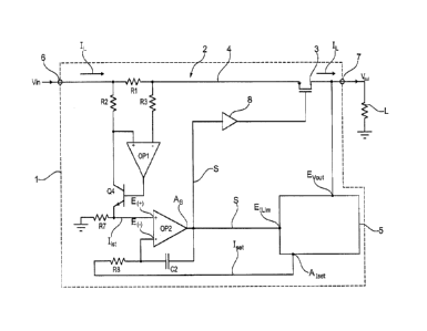
The schematically shown electronic circuit breaker 1 includes a voltage-
controlled
current source 2 with a power transistor or semiconductor switch 3 in a
positive current
path 4 and includes a control unit or control device 5, for example in the
form of a
microcontroller. The current path 3 extends between an operating voltage
terminal or
voltage input 6 and a (positive) load terminal or load output 7. To this is
connected the
positive pole of a load L that is to be switched, while the negative pole
thereof is routed
to earth or ground. The operating voltage or input voltage Vin, in the form
of, e.g., a DC
voltage at 24V (DC), is applied to the voltage input 6 of the electronic
circuit breaker 1.
The controllable semiconductor switch 3 in the exemplary embodiment is
implemented
by a so-called PMOS (p-channel MOSFET or PMOSFET), which is to say a metal
oxide
semiconductor field-effect transistor in which positively charged charge
carriers (defect
electrons) are used to conduct electric current through the channel.
During operation of the circuit breaker 1 with the DC voltage source connected
and load
L connected, a load current starting from the voltage input 6 flows through
the current
path 3, and thus through the drain-source section of the semiconductor switch
3 and
through the load L, to the reference potential or ground. This load current
flowing
through the semiconductor switch 3 and through the load L corresponds to the
output
current IL of the voltage-controlled current source circuit 2. The output
current IL is
sensed by means of the voltage-controlled current source circuit 2. To this
end, the
latter includes the resistors R1 to R3 and the operational amplifier OP1, as
well as the
= CA 03000877 2018-04-04
9
transistor 04 and the resistor R7 that is routed to ground or the reference
potential, in
the connection thereof shown in Figure 1.
Using the resistors R1, R2, R3 and the operational amplifier OP1, as well as
using the
transistor Q4 and using the resistor R7, which is connected to ground, of the
voltage-
controlled current source circuit 2, a type of current mirroring occurs in
that the output
current IL flowing through the resistor R1 is, as it were, mirrored at the
resistor R7 at a
comparatively low current level. If the output current is, e.g., 1 A, then the
current
flowing through the resistor R7 is 1 mA, for example. The corresponding
voltage value
at the resistor R7 is fed to the positive input of the operational amplifier
0P2 as the
actual value list of the output current IL.
The voltage-controlled current source circuit 2 comprises primarily an
operational
amplifier 0P2 operating as a comparator for subtraction, to whose (positive)
input EN
the resistor R7, and thus the actual value list of the output current IL, is
routed. The
inverting input E(..) of the operational amplifier 0P2 is routed through a
resistor R8 to an
output Aiset of the control unit 5. The control unit 5 provides a setpoint
value [set of the
output current IL to the operational amplifier 0P2 through the output Aiset. A
capacitor C2
is wired between the output As and the inverting input Eo of the operational
amplifier
OP2.
The output As of the operational amplifier 0P2 of the voltage-controlled
current source
circuit 2 is routed to an input ElLim of the control unit 5. Another input
Evout of the control
unit 5 is routed to the current path 4 between the semiconductor switch 3 and
the load
terminal 7. Moreover, the output As of the operational amplifier 0P2 of the
current
source circuit 2 is connected to the semiconductor switch 3 on the control
side, which is
to say to its control input (gate). In the exemplary embodiment, this is
accomplished by
means of an amplifier 8 of the voltage-controlled current source circuit 2.
In the normal operating state of the electronic circuit breaker 1 and of its
voltage-
controlled current source circuit 2, the output Aiset of the control unit 5,
and thus the
= CA 03000877 2018-04-04
setpoint value lset, are set such that the output current IL preferably is
greater than the
maximum load current. Under these normal conditions, the load voltage or
output
voltage Vout of the electronic circuit breaker 1 will be equal to its input
voltage V.
In the event of an overload or short circuit or during a switch-on to a
capacitive load L,
initially the output current IL is actively limited to a nominal value INom in
that the
semiconductor switch 3 is driven accordingly. This state is detected by the
control unit 5
because it is connected to the output As of the operational amplifier 0P2,
which
produces the difference between the present actual value list and the
predefined
setpoint value !sot, and which at its output supplies a correspondingly
altered difference
value S as a control signal (control voltage) for the semiconductor switch 3.
This altered
difference value S of the operational amplifier 0P2 results in a corresponding
driving of
the semiconductor switch 3, so that the latter is appropriately driven off and
the output
current IL is limited to a current limiting value !max. The overload or short
circuit condition
is also detected by the control unit 5 using the changing output voltage (load
voltage)
Vout.
As soon as the overload or short circuit is detected, the output current IL of
the voltage-
controlled current source circuit 2 is set by suitably changing the setpoint
value Iset such
that the maximum power dissipation Pmax of the semiconductor switch 3 lies
within its
safe operating area (safe operation area). At the same time, the output
voltage VOW is
monitored.
If the output voltage Vout does not rise within a predefinable time period,
the output
current IL is set to zero (0 A), which is to say that the electronic circuit
breaker 1
switches off the load output or load terminal 7.
In contrast, if the output voltage Vout rises, the setpoint value lset is
increased, preferably
stepwise, within the safe operating area of the semiconductor switch 3, so
that the
output current IL also rises in corresponding stepwise fashion. During this
process, the
power, which is to say the power dissipation of the semiconductor switch 3,
always
CA 03000877 2018-04-04
11
remains less than or equal to a maximum power value Pmax. This is accomplished
by
means of the control unit 5, by taking the product (Vout = !set) of the
setpoint value Iset and
the output voltage Vt. The increase in the setpoint value !set within the
permissible
power range of the semiconductor switch 3 preferably takes place incrementally
until
the output voltage Vout is again equal to the input voltage Vin of the
electronic circuit
breaker 3 or its current source circuit 2.
This control method, which is suitable even for switch-on of the electronic
circuit breaker
1 to a capacitive load L, in particular, is illustrated in the flow chart
shown in Fig. 2. After
the start, which is to say upon switch-on of the electronic circuit breaker 1,
the setpoint
value Iset is set to the applicable nominal current INom by the control unit
5. This is
followed by the check as to whether the setpoint value Iset that has been set
is greater
than the current limiting value or maximum value Imax. If this is the case,
then in the next
step the product is taken of the present setpoint value !set and the present
output voltage
Vout, and a check is made as to whether this product is greater than the
maximum
power value Pmax. If this is the case, the setpoint value 'set is set to a
minimum value Wm.
This value preferably corresponds to a fraction, for example 20%, of the
nominal value
INom of the output current IL.
Fig. 4 shows this state using the diagram of current INom(t) vs. time, where
time tin ps is
plotted on the x-axis and the normalized load current or output current IL is
plotted on
the y-axis as nominal value INom (in %). In the initial state, the setpoint
value Iset is set to
the nominal value INom of the output current IL. This state is maintained as
long as the
setpoint value !set is less than the maximum value !max and the power (Vout =
!set) of the
semiconductor switch 3 is less than the maximum power value Pmax.
The switch-on of the electronic circuit breaker 1 to the capacitive load L
takes place at
the time t = 400. At more or less the same time, the control unit 5 sets the
setpoint value
'set of the output current IL to 20% of the nominal value INom. With the
lowering of the
setpoint value Iset, the semiconductor switch 3 is correspondingly driven off
by the
operational amplifier 0P2 using the difference value S. After a predefinable
time period,
CA 03000877 2018-04-04
12
for example with At = 100, the response to this setting or control or
regulation is sensed
in that the present output voltage Vout (t = 500) is checked. If the output
voltage is zero
(Vout = 0), then the electronic circuit breaker 3 trips. In contrast, if the
output voltage is
nonzero (Vout 0 0), which is to say if the output voltage Vout has reached a
certain
voltage value Vt > 0, then the setpoint value Iset is increased by a step
value Istep, which
corresponds to 30% of the normal current INom, for example.
This is followed by the check as to whether the setpoint value 'set has
already reached
the normal value INom. If this is the case, the control algorithm starts again
with the
check as to whether the setpoint value 'set corresponds to the nominal value
INom. If this
is not the case, the program sequence is run, starting with another setpoint
value
increase Istep, along with a query as to the output voltage Vout and, in
particular, its rise
as a result of the stepwise increase in the setpoint value Iset. If the output
voltage Vout
does not exceed the voltage value Vt, then tripping of the electronic circuit
breaker 3
takes place again.
The relationship between the successive, preferably stepped, increase in the
setpoint
value Iset, and thus the output current IL on the one hand and the behavior
over time of
the normalized load voltage or output voltage Vout(%) on the other hand, is
evident from
the diagrams shown in Fig. 3 and 4. Accordingly, if the output current IL, and
along with
it the output voltage Vout as well, rises continuously with the successive
increase in the
setpoint value !set, then the setpoint value Iset is increased until the
output current IL
reaches the nominal value INom. The voltage curve over the time tin ps shown
in Fig. 4
represents the typical case of switch-on to a capacitive load L.
By means of the method, and on the basis of the algorithm corresponding to the
flowchart shown in Fig. 2, the semiconductor switch 3 can be driven within the
framework of constant current limiting such that the output current or load
current IL is
limited at least briefly to a predefined maximum current limiting value Imax
in the event of
an overload or short circuit, and such that the power dissipation of the
semiconductor
switch is less than or equal to the maximum power value Pmax as this takes
place. The
CA 03000877 2018-04-04
= =
13
current limiting value Imax is, for example, 1.5 to 2 times the nominal
current of the circuit
breaker 1.
As a result of the provision of the setpoint value [set by the control unit 5
to the
operational amplifier 0P2, and thus to the voltage-controlled current source
circuit 2, the
power of the semiconductor switch 3 is monitored by the control unit 5 in all
operating
states. In this way, the semiconductor switch 3 can be dimensioned
commensurately
smaller with regard to the power dissipation that must be handled.
In the case of the voltage-controlled current source circuit 2 that
advantageously
operates according to the exemplary embodiment with the actual / setpoint
comparison
using a PMOS field-effect transistor, current limiting takes place almost
automatically in
the event of an overload or short circuit by the means that the semiconductor
switch 3 is
automatically driven off when a threshold value is reached or exceeded due to
the
production of the difference value S at the output As of the operational
amplifier 0P2.
Thus, the difference value S, which is to say the voltage difference value
driving the
semiconductor switch 3 as a control signal, is less than zero (< OV) in normal
operation.
In this state the control unit 5 can be quiescent and is correspondingly low
power. Only
when the difference value S exceeds the threshold value So, namely So = 0 V,
or in
other words is greater than zero, does the control unit 5 react and lower the
setpoint
value 'set, with the semiconductor switch 3 being driven beforehand or at the
same time
into current limiting with IL 5 !max by means of the difference value S So.
The invention is not limited to the exemplary embodiment described above.
Rather,
other variants of the invention can also be derived herefrom by a person
skilled in the
art without departing from the subject matter of the invention. In particular,
moreover, all
individual features described in connection with the exemplary embodiments may
also
be combined with one another in other ways without departing from the subject
matter
of the invention.
' = CA 03000877 2018-04-04
14
Thus, for example, a different type of MOSFET or bipolar transistor can be
used as the
semiconductor switch 3 in place of the PMOS transistor. In addition, the
amplifier 8 can
be omitted or can be constructed as an amplifier circuit.
= CA 03000877 2018-04-04
List of Reference Characters
1 electronic circuit breaker
2 voltage-controlled current source circuit
3 semiconductor switch
4 current path / positive path
5 control unit / control device
6 voltage input
7 load terminal / load output
8 amplifier
Alset output
As output
C1,2 capacitor
E(+) (positive) input
E(-) inverting input
Evout input
ElLim input
load
OP1,2 operational amplifier
Q2,4 transistor
R1-R8 ohmic resistor
IL output current / load current
'max maximum value / current limiting value
INfin minimum value
INom nominal value
'set setpoint value
Vin operating voltage / input voltage
N/out output voltage
Pmax maximum power value
difference value / control signal
CA 03000877 2018-04-04
16
So threshold value