Note: Descriptions are shown in the official language in which they were submitted.
OPTICAL FILTER WITH SELECTIVE TRANSMITTANCE AND REFLECTANCE
RELATED APPLICATIONS
[0001] This paragraph has been intentionally left blank.
FIELD OF THE INVENTION
[0002] The present invention relates to optical filters and, more
particularly, to optical
filters having selective transmittance and tunable, differential front and
back surface
reflectance, optical articles employing the same, and methods of forming
thereof.
BACKGROUND OF THE INVENTION
[0003] It is known in the art that ultraviolet (UV), wavelengths of light
between 280 nm and
380 nm under ANSI standards and 400 nm under other AUS/NZ standards, are
harmful
to the human eye. More recently, it has also started to become apparent that
high energy
visible light, HEV, which is characterized as having wavelengths from 400 nm
up to 500
nm, also poses possible threats to eye health and other living tissue. This
risk occurs at
the highest energies, or lowest wavelength, of the HEV spectrum. This light
range has
also been attributed to other beneficial biological factors such as regulation
of circadian
rhythms. Hence, applications are being developed to selectively reduce and
or/control
these high energy, UV and HEV wavelengths incident upon the eye. One approach
to
reducing UV and HEV wavelength incident upon the eye is to employ optical
filters in or
on eyewear.
[0004] Such filters can be created in a variety of ways, including through
physical vapor
deposition, PVD, techniques. Coatings to reduce and control the reflection
from the
surface of a lens, referred to as antireflection, AR, coatings are commonly
employed.
Examples of AR coatings can be found in U.S. Patents Nos. 6,165,598 to Nelson;
8,425,035 to Blunckenhagen; 8,007,901 to Beinat; and 6,768,581 to Yip.
Macleod, Angus;
Thin Film Optical Filters (3rd
1
Date Recue/Date Received 2022-04-07
Edition); 10P, 2001 provides detailed information and theory behind the design
of AR
coatings and optical filters.
[0005] Common considerations in the forming of AR coatings are 1) achieving
high
transmission throughout the visible spectrum, e.g. from 380 to 780 nm; 2)
achieving a
neutral or appealing reflected color; 3) controlling of off angle color; and
4) providing layers
in or on the coating for improved cleanability, e.g. hydrophobicity or
oleophobicity.
[0006] Generally, AR coatings employ alternating layers of at least two
materials. The
materials are chosen such that one material has a refractive index of less
than 1.6, e.g.
silicon dioxide, SiO2, and the other material has a refractive index greater
than 1.6, e.g.
titanium dioxide, TiO2, or, zirconium dioxide, ZrO2. More than two different
materials may
also be employed to achieve the desired characteristics of the coating. In
addition, a
conductive layer may be employed, such as indium tin oxide, as described in
U.S. Pat.
No. 6,852,406 to Marechal, or a thin metallic layer, such as 0.2 nm of Au, as
described in
U.S. Pat. No. 8,007,901 to Beinat, to impart anti-static properties to the
coating. In these
cases, the conductive layer is chosen to maximize transmission while
maintaining the
required anti-static property, i.e. absorption of light by the layer is
minimized to be less
than 5 percent through the visible, for example, less than 1 percent.
[0007] In an optical filter system, light is transmitted (T), reflected (R) or
absorbed (A). If
the total incident light intensity is lc, then:
/0= T + R +A.
[0008] Furthermore, as described in Macleod, transmission is invariant, i.e.
remains
constant and does not depend on which side of a lens one is looking. Absent
absorption
in the substrate, e.g. optical lens material, the above relationship creates a
situation in
which the reflection from the front of a lens and the back of the lens must be
equal. The
above referenced patents do not contain any appreciable absorption in the
visible portion
of the spectrum since they are constructed from transparent dielectric
materials.
Therefore, the reflection is identical when viewed from either side of the
lens, ignoring any
effect of the substrate.
2
Date Recue/Date Received 2021-10-08
[0009] This poses a challenge for the design of optical filters for blocking
HEV portions of
the spectrum. The most common method of blocking such wavelengths is through
an edge
filter that has a high reflection below a specified wavelength and low
reflection above this
wavelength. However, achieving a high front surface reflection necessarily
results in a
high back surface reflection, even from a coating applied to only a front of a
lens. Hence,
the HEV wavelengths will be reflected into the eye from the back surface. In
certain
applications, this problem can become more acute. For example, the intensity
of blue
emission from modem HID headlamps on cars can be very distracting to drivers
of
oncoming cars. The blue light of the HID headlamp is scattered on surfaces
leading to
glare. This problem gets worse with the age of the driver. The use of an
"edge" optical
filter on eye glasses can help to reduce this problem by reflecting the blue
light from the
front of the lens. However, light from cars behind the driver will be
reflected into the eyes.
This is true even if the edge filter is only applied to the front of the lens,
especially since
most optical lens materials will not preferentially attenuate blue light. This
effect can be
very distracting to drivers and can even momentarily blind a driver due to
passing cars.
[0010] U.S. Pat. No. 8,870,374 to Cado attempts to address this problem in the
context
of UV light by providing front and back reflection of a lens that differ in
their respective UV
spectrum. This approach is based upon the UV absorption inherent in the lens
material
employed and upon the application of different AR coatings on the front and
the back of
the lens. Specifically, a low UV reflection AR is applied to the back of the
lens to prevent
reflection into the wearers eyes. The front AR can be independently designed
and UV
blocking provided by the lens material_ Therefore, the ability to achieve
efficient UV
blocking requires the substrate or lens to provide efficient blocking
characteristics.
Furthermore, the designs shown in Cado have symmetric reflections from the
front and
back of the AR coatings from each of the coatings, ignoring any absorption in
the
substrate.
[0011] U.S. Pat. No. 3,679,291 to Apfel describes coatings employing absorbing
layers
to influence the back reflection and front reflection from a surface
independently. In this
context "front" refers to the side of the lens containing the optical coating,
i.e. one side of
the coating is air and the other side of the coating is proximate the
substrate or lens, and
back is the surface opposing the optical
3
Date Recue/Date Received 2021-10-08
CA 03001120 2018-04-05
WO 2017/066473 PCMJS2016/056882
coating. The design demonstrates large differences in the front and back
reflections,
however, with a highly undesirable transmission that is lower than 60 percent.
Furthermore, the designs in Apfel are limited to broad transmission throughout
the visible
spectrum. U.S. Pat. No. 5,521,759 to Dobrowolski describes employing absorbing
layers
in a filter design with the specific purpose of side band suppression in notch
transmission
filters, however, also without specific concern for maintaining transmission.
[0012] Hence, there exists a need in the field for alternate filter designs
and systems
that independently controls the reflection of desired wavelengths of light
from the front
and the back surfaces of a lens, that is independent of any absorption that
may be present
in the lens material, that does not require application of both front side and
backside
coatings, and, hence, that is more economical to produce. There also exists a
need in
the field for alternate filter designs for other optical and aesthetic
effects, such as
achromaticity, without concern for increasing the back reflection into the
eye.
OBJECTS AND SUMMARY OF THE INVENTION
[0013] The present invention provides optical filters, filter designs, and
optical article
and systems that independently controls the reflection of desired wavelengths
of light from
the front and the back surfaces of the filter or optical article, that is
independent of any
absorption that may be present in the substrate of the optical article, that
does not require
application of both front side and backside coatings on the optical article,
and, hence, that
is more economical to produce. These objectives are achieved, in part, by
providing an
optical filter comprising; a plurality of alternating layers of transparent
dielectric materials
having different refractive indices; at least one layer of a metallic
absorbing material
having a thickness of less than 50 nm; and a percent transmission of the
optical filter
greater than 70 percent. The plurality of alternating layers of transparent
dielectric
materials comprising a material having a refractive index of less than or
equal to 1.6. The
plurality of alternating layers of transparent dielectric materials comprising
a material
having a refractive index of greater than 1.6. The at least one layer of a
metallic absorbing
material comprising a conductive material. The at least one layer of a
metallic absorbing
material comprising gold, titanium nitride and/or zirconium nitride. The at
least one layer
of a metallic absorbing material interposed directly between two layers of the
plurality of
alternating layers of transparent dielectric materials having different
refractive indices.
¨4¨
CA 03001120 2018-04-05
WO 2017/066473 PCT/1JS2016/056882
The at least one layer of a metallic absorbing material interposed directly
within a layer of
the plurality of alternating layers of transparent dielectric materials. The
at least one layer
of a metallic absorbing material positioned within the plurality of
alternating layers of
transparent dielectric materials towards a front side of the optical filter.
The at least one
layer of a metallic absorbing material positioned within the plurality of
alternating layers of
transparent dielectric materials towards a backside of the optical filter.
[0014] These objectives are further achieved, in part, by providing an
ophthalmic lens
comprising a lens substrate; and an optical filter having a front surface and
a back surface
attached to a front surface of the lens substrate; a percent reflectance from
a front surface
of the ophthalmic lens 50 percent greater than a percent reflectance from the
back surface
of the optical filter. Wherein, the lens substrate is thermoplastic. Wherein,
the lens
substrate is a curable liquid monomer mixture or a curable urethane based
prepolymer
composition. The ophthalmic article further comprising a functional laminate.
The optical
filter comprising a plurality of alternating layers of transparent dielectric
materials having
different refractive indices; and at least one layer of a metallic absorbing
material having
a thickness of less than 50 nm. The optical filter comprising at least one
layer of gold,
titanium nitride and/or zirconium nitride.
[0015] These objectives are further achieved, in part, by providing a
method for
forming an optical article comprising: obtaining an optical substrate;
applying at least one
layer of transparent dielectric material having a refractive index above 1.6
on a surface of
the optical substrate; applying at least one layer of transparent dielectric
material having
a refractive index less than or equal to 1.6 on the surface of the optical
substrate; applying
at least one layer of a metallic absorbing material on the surface of the
optical substrate;
and imparting a percent reflectance from a front surface of the optical
article 50 percent
greater than a percent reflectance from a backside of the front surface of the
optical article
through the applying the at least one layer of a metallic absorbing material.
The applying
at least one layer of a metallic absorbing material comprising applying a
layer having a
thickness of less than 50 nm. The applying at least one layer of a metallic
absorbing
material comprising applying a conductive material. The applying at least one
layer of a
metallic absorbing material comprising applying gold, titanium nitride and/or
zirconium
¨5¨
nitride. The obtaining an optical substrate comprising obtaining a
thermoplastic ophthalmic
lens.
[0015a] According to another aspect, there is provided an ophthalmic lens
comprising:
a lens substrate; and
an optical filter having a front surface and a back surface attached to a
front
surface of the lens substrate:
the optical filter further comprising alternating layers where at least one of
the
alternating layers is a transparent dielectric material having a refraction
index
above 1.6 and at least another one of the alternating layers is a transparent
dielectric material having a refraction index of 1.6 or less; and
the optical filter further comprising at least one absorbent layer of an
absorbent
material including a metal such that a percent reflectance from a front
surface of
the ophthalmic lens is 30 percent greater than a percent reflectance from the
back
surface of the optical filter.
[0015b] According to another aspect, there is provided a method for forming an
optical
article comprising:
obtaining an optical substrate;
forming an optical filter on the optical substrate comprising:
applying at least one layer of transparent dielectric material having a
refractive
index above 1.6 on a surface of the optical substrate;
applying at least one layer of transparent dielectric material having a
refractive
index less than or equal to 1.6 on the surface of the optical substrate; and
applying at least one layer of a metallic absorbing material on the surface of
the optical substrate; and
imparting a percent reflectance from a front surface of the optical article 30
percent greater than a percent reflectance from a backside of the optical
filter
through said applying the at least one layer of a metallic absorbing material.
[0015c] According to another aspect, there is provided an optical filter
comprising:
a plurality of alternating layers of transparent dielectric materials having
different refractive indices;
at least one layer of a metallic absorbing material having a thickness of less
than 50 nm such that a percent reflectance from a front surface of the optical
filter is
6
Date Recue/Date Received 2022-04-07
30 percent greater than a percent reflectance from a back surface of the
optical filter;
and
a percent transmission of the optical filter greater than 70 percent.
[0015d] According to another aspect, there is provided an ophthalmic lens
comprising:
a lens substrate;
an optical filter having a front surface and a back surface attached to a
front surface
of the lens substrate; and
a percent reflectance from a front surface of the ophthalmic lens 30 percent
greater
than a percent reflectance from the back surface of the optical filter;
wherein said optical filter has an average transmission for light having
wavelengths
in the range of 500-800 nm of greater than 70 percent.
[0015e] According to another aspect, there is provided a method for forming an
optical
article comprising:
obtaining an optical substrate;
forming an optical filter on the optical substrate comprising:
applying at least one layer of transparent dielectric material having a
refractive
index above 1.6 on a surface of the optical substrate;
applying at least one layer of transparent dielectric material having a
refractive
index less than or equal to 1.6 on the surface of the optical substrate;
applying at least
one layer of a metallic absorbing material on the surface of the optical
substrate; and
imparting a percent reflectance from a front surface of the optical article 30
percent
greater than a percent reflectance from a backside of the optical filter
through the
applying the at least one layer of the metallic absorbing material;
wherein said optical filter has an average transmission for light having
wavelengths
in the range of 500-800 nm of greater than 70 percent.
BRIEF DESCRIPTION OF THE DRAWINGS
[0016] These and other aspects, features and advantages of which embodiments
of the
invention are capable of will be apparent and elucidated from the following
description of
embodiments of the present invention, reference being made to the accompanying
drawings, in which
6a
Date Recue/Date Received 2022-04-07
[0017] Fig. 1 is a partial cross-sectional view of an optical article
according to one
embodiment of the present invention.
[0018] Fig. 2 is a graph comparing n and k values for tungsten and gold.
[0019] Fig. 3A is a partial cross-sectional view of an optical filter
according to one
embodiment of the present invention.
[0020] Fig. 3B is a partial cross-sectional view of an optical filter
according to one
embodiment of the present invention.
[0021] Fig. 3C is a partial cross-sectional view of an optical filter
according to one
embodiment of the present invention.
[0022] Fig. 4A is a table showing the configuration of an optical filter
according to one
embodiment of the present invention.
[0023] Fig. 4B is a graph showing the transmittance of an optical filter
according to one
embodiment of the present invention.
[0024] Fig. 4C is a graph showing the front side reflectance of an optical
filter according
to one embodiment of the present invention.
[0025] Fig. 4D is a graph showing the backside reflectance of an optical
filter according
to one embodiment of the present invention.
6b
Date Recue/Date Received 2022-04-07
CA 03001120 2018-04-05
WO 2017/066473 PCT/1JS2016/056882
[0026] Fig. 5A is a table showing the configuration of an optical filter
according to one
embodiment of the present invention.
[0027] Fig. 5B is a graph showing the transmittance of an optical filter
according to one
embodiment of the present invention.
[0028] Fig. 5C is a graph showing the front side reflectance of an optical
filter according
to one embodiment of the present invention.
[0029] Fig. 5D is a graph showing the backside reflectance of an optical
filter according
to one embodiment of the present invention.
[0030] Fig. 6A is a graph showing the transmittance, front side
reflectance, and
backside reflectance of an optical filter according to one embodiment of the
present
invention.
[0031] Fig. 6B is a graph showing the transmittance, front side
reflectance, and
backside reflectance of an optical filter according to one embodiment of the
present
invention.
[0032] Fig. 7A is a table showing the configuration of an optical filter
according to one
embodiment of the present invention.
[0033] Fig. 7B is a graph showing the front side reflectance of an optical
filter according
to one embodiment of the present invention.
[0034] Fig. 7C is a graph showing the backside reflectance of an optical
filter according
to one embodiment of the present invention.
[0035] Fig. 8A is a table showing the configuration of an optical filter
according to one
embodiment of the present invention.
[0036] Fig. 8B is a graph showing the front side reflectance of an optical
filter according
to one embodiment of the present invention.
[0037] Fig. 8C is a graph showing the backside reflectance of an optical
filter according
to one embodiment of the present invention.
¨7¨
CA 03001120 2018-04-05
WO 2017/066473 PCMJS2016/056882
[0038] Fig. 9A is a table showing the configuration of an optical filter
according to one
embodiment of the present invention.
[0039] Fig. 9B is a graph showing the transmittance, front side
reflectance, and
backside reflectance of an optical filter according to one embodiment of the
present
invention.
[0040] Fig. 90 is a graph showing the transmittance, front side
reflectance, and
backside reflectance of an optical filter according to one embodiment of the
present
invention.
[0041] Fig. 9D is a graph showing the transmittance, front side
reflectance, and
backside reflectance of an optical filter according to one embodiment of the
present
invention.
[0042] Fig. 9E is a graph showing the transmittance, front side
reflectance, and
backside reflectance of an optical filter according to one embodiment of the
present
invention.
[0043] Fig. 9F is a graph showing the transmittance, front side
reflectance, and
backside reflectance of an optical filter according to one embodiment of the
present
invention.
[0044] Fig. 9G is a graph showing the transmittance, front side
reflectance, and
backside reflectance of an optical filter according to one embodiment of the
present
invention.
[0045] Fig. 9H is a graph showing the transmittance, front side
reflectance, and
backside reflectance of optical filters according to certain embodiments of
the present
invention.
[0046] Fig. 10A is a table showing the configuration of an optical filter
according to one
embodiment of the present invention.
[0047] Fig. 10B is a graph showing the transmittance of an optical filter
according to
one embodiment of the present invention.
¨8¨
CA 03001120 2018-04-05
WO 2017/066473 PCMJS2016/056882
[0048] Fig. 100 is a graph showing the front side reflectance of an optical
filter
according to one embodiment of the present invention.
[0049] Fig. 10D is a graph showing the front side reflectance of an optical
filter
according to one embodiment of the present invention.
[0050] Fig. 11A is a table showing the configuration of an optical filter
according to one
embodiment of the present invention.
[0051] Fig. 11B is a graph showing the transmittance of an optical filter
according to
one embodiment of the present invention.
[0052] Fig. 110 is a graph showing the front side reflectance of an optical
filter
according to one embodiment of the present invention.
[0053] Fig. 11D is a graph showing the front side reflectance of an optical
filter
according to one embodiment of the present invention.
DESCRIPTION OF EMBODIMENTS
[0054] Specific embodiments of the invention will now be described with
reference to
the accompanying drawings. This invention may, however, be embodied in many
different
forms and should not be construed as limited to the embodiments set forth
herein; rather,
these embodiments are provided so that this disclosure will be thorough and
complete,
and will fully convey the scope of the invention to those skilled in the art.
The terminology
used in the detailed description of the embodiments illustrated in the
accompanying
drawings is not intended to be limiting of the invention. In the drawings,
like numbers refer
to like elements.
[0055] Broadly speaking, the present invention relates to coating designs,
for example
vapor deposition coatings, that provide improved control over the
transmittance and the
front and backside reflectance of an optical filter by providing controlled
absorption
through inclusion of one or more absorption layers within the coating or
coating stack
forming the optical filter. The present invention provides several advantages:
(1)
wavelength blocking can be accomplished by a combination of reflection and
absorption;
(2) front and backside reflectances from a coating can be influenced
independently; (3)
¨9¨
CA 03001120 2018-04-05
WO 2017/066473 PCMJS2016/056882
color appearance can be manipulated in order to create new mirrors or tints;
and (4)
enhanced Bayer or environmental performance can be provided through the use of
alternate materials.
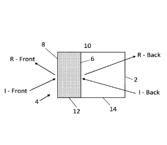
[0056] The concept of front and backside coating reflection is shown in
Fig. 1. In
certain embodiments, an inventive coating 12 is applied to one side of an
optical substrate
14. A front side 8 of the coating 12 is the side opposite the substrate 14. A
backside 6 of
the coating 12 is the side in contact with the substrate 14. The front side 8
of the coating
12 may, but need not necessarily, correlate with a front side 4 of an optical
article 10.
Light incident on the front of the optical article 10, I-Front, can be
reflected and is referred
to as front side reflection, R-Front. Light incident on the backside 6 of the
coating 12, I-
Back, may also be reflected and is referred to as the backside coating
reflection, R-Back.
It is important to note the backside coating reflection, R-Back, does not
originate at the
backside 2 of the substrate 14 but rather at the interface of the backside 6
of the coating
12 and the substrate 14.
[0057] Certain potential performance characteristics of a filter design
with absorbing
layers can be understood through the concept of "Potential Transmittance", as
described
by MacLeod. As previously mentioned, light must be either transmitted (T),
reflected (R),
or absorbed (A). Often the purpose of a filter coating is to achieve a minimum
in reflection,
in order to maximize transmittance. If one has an existing optical filter with
a given
transmission and reflection, the maximum transmission that can be possibly
attained by
adding layers to the front and/or back of the filter is the potential
transmittance (y), given
by:
1¨R) T +A
[0058] Therefore, the potential transmittance is ultimately limited by the
amount of
absorption present in the stack if the reflectance is eliminated. The
absorption is in part
dependent upon the refractive index of the absorbing layer included in the
optical stack.
For example, a 10 nm thick layer of tungsten on glass will have an average
potential
transmittance of 43 percent from 500-800 nm. In contrast a 10 nm layer of gold
will have
¨ 10 ¨
CA 03001120 2018-04-05
WO 2017/066473 PCMJS2016/056882
an average potential transmittance of 90 percent over the same range of 500-
800 nm.
These values are critical in consideration of a pass band region of a filter.
[0059] For a broad band visible filter, similar to what might be used in
sunglasses a
minimum potential transmittance of 8% over the visible spectrum (380 to 780
nm) would
be dictated by regulatory limits for general purpose sun lenses. An upper
potential
transmittance limit for this broadband filter would be less than 80 percent
which defines
the start of light tinting for sun wear. Most common and preferred would be
potential
transmission levels of less than 50 percent, which is most common for sun
wear. This,
therefore, defines the range of the absorption to be from 20-92 percent for a
broad band
sun wear application, implying the reflection from the back of the lens is at
or near zero
maximizing the transmission. The front reflection would be substantially
higher and
nominally range from 20 to 80 percent.
[0060] Of more interest is the creation of edge filters to block specific
spectral regions.
A material such as gold can have a high maximum potential transmittance from
500-800
nm (greater than 90 percent for a thickness of 10 nm, 86 percent for a
thickness of 15 nm)
while having a lower potential transmittance in portions of the HEV region,
for example
400-450 nm (62 percent for a thickness of 10 nm and 53 percent for a thickness
of 15
nm). This difference in potential transmittance facilitates creating filters
with high
transmission in a pass band (for example greater than 80 percent from 500-800
nm and
preferably greater than 90 percent from 500-800 nm). Simultaneously, the
filter would
have a stop band region with a reflection from the back of the filter lower
than 20 percent,
and preferably lower than 10 percent while maintaining a front filter
reflection greater than
70 percent and preferably greater than 80 percent. This is possible due to the
presence
of the absorption in the optical filter. The design creates an asymmetry in
the absorption
and therefore reflection depending on which direction the light is entering
the filter (from
the front or the back).
[0061] The absorbing materials employed in the present invention can be
broadly
grouped into two categories: (1) conductors in which the free carriers can
generate
absorption, e.g. metals and transparent conductive oxides, TOO, and (2) band
edge
absorbers, e.g. semiconductors or low band-gap insulators such as titanium
dioxide, Ti02.
Over the near UV and visible wavelengths, metals can be broadly grouped into
two
¨11¨
CA 03001120 2018-04-05
WO 2017/066473 PCMJS2016/056882
categories: (1) those with low "n", refractive index, and high "k",
absorptance; and (2)
those with comparable n and k values. Fig. 2 shows a graph comparing n and k
values
for Tungsten (W) and Gold (Au), materials which represent two distinct n and k
profiles.
[0062] The significance of this grouping is that metal films of the same
thickness with
high k/n ratio will have a much higher potential transmittance relative to
metals with a
lower k/n ratio. Therefore, in certain embodiments, filters and filter designs
are provided
which can have a high transmittance over a given spectral range and then a
lower
transmittance outside this range. In certain embodiments, coatings according
to the
present invention employ absorbers or absorbing layers that, when selectively
located
and formed within the coating system, allow for the creation of filters with a
desired
transmittance and a low reflectance. Furthermore, certain embodiments of the
present
invention provide for the isolation or enhancement of this effect to one side
of a lens (i.e.
the front and back reflectance's can be made different) and/or the creation of
a reflectance
on a front and a back side of the optical article or lens.
[0063] In certain embodiments, the design approach of the present invention
is, in part,
dependent on the choice of absorbing materials. For example, metals with a
high k/n
ratio, e.g. aluminum, silver, gold, allow high potential transmittance while
lower k/n ratio
materials allow a lower potential transmittance but are more neutral in
appearance.
[0064] In certain embodiments, an absorbing layer is incorporated into a
coating stack
to reduce both the front and back reflection while maintaining a low
transmission in a
select band, i.e. a blocking or rejection band. For example, by absorbing HEV
wavelengths the reflected color, typically violet for HEV blocking, is altered
to be
aesthetically more appealing while maintaining the desired protection.
[0065] In certain embodiments, selective blocking filters, such as for
filtering HEV
wavelengths, are provided in which an absorber is incorporated into a coating
stack in
order to achieve high reflectance below a cutoff wavelength from the front
surface, a
significantly reduced back reflectance below a cutoff wavelength from the eye
side of the
lens, and high transmittance through the visible wavelengths.
[0066] In certain embodiments of the present invention, a filter is formed,
in part, of
one or more layers of absorbing material interposed within alternating layers
of one or
¨12¨
CA 03001120 2018-04-05
WO 2017/066473 PCMJS2016/056882
more materials selected from, but not limited to, materials including: silicon
dioxide, silicon
oxynitride, aluminum oxide, titanium dioxide, tantalum pentoxide, and
zirconium dioxide.
In certain embodiments, a layer of absorbing material is interposed directly
between a
layer of high refractive index material and a layer of low refractive index
material. In
certain other embodiments, a layer of absorbing material is directly
interposed within an
otherwise single, contiguous layer of high or low refractive index material.
[0067] In certain embodiments of the present invention, optical filters and
optical
articles formed thereof are provided (1) that have an average transmission for
light having
wavelengths in the range of 500-800 nm of greater than 70 percent, for
example, in the
range of approximately 70 to 99 percent, 80 to 99 percent, 90-99 percent; (2)
that have a
backside reflectance of the coating forming the filter for light having
wavelengths in the
range of 400-450 nm of less than 40 percent, less than 30 percent, less than
10 percent,
or less than 2 percent or in the range of approximately 5-65 percent; (3) that
have a front
side reflectance for light having wavelengths in the range of 400-450 nm of in
the range
of approximately 50-90 percent or 75-90 percent.
[0068] In certain embodiments of the present invention, optical filters and
optical
articles formed thereof are provided that have a difference between the
backside
reflectance of the coating and the front side reflectance of the coating
and/or optical article
employing the coating above 50 percent or in the range of approximately 30-85
percent.
[0069] As shown in Figs. 3A-30, according to certain embodiments, a lens or
optical
article 10 has a coating 12, i.e. has an optical filter stack. For the sake of
clarity, the
coatings or stacks disclosed herein will be described from the bottom up. That
is to say,
the various layers forming the coating or stack will be described starting
from a first or
bottom layer of the stack that is applied directly to an optical substrate and
proceeding
sequentially with each subsequent layer of the stack applied. In this manner,
a "top layer"
of the coating or stack is the last layer of the relevant coating or stack
applied during the
coating process.
[0070] In the embodiment shown in Fig. 3A, a first high refractive index
layer 16 is
applied directly on top of an optical substrate 14. A metallic absorbing layer
20 is applied
directly on top of the first high refractive index layer 16. A first low
refractive index layer
¨ 13 ¨
CA 03001120 2018-04-05
WO 2017/066473 PCT/1JS2016/056882
18 is applied directly on top of the absorbing layer 20. A second high
refractive index
layer 16 is applied directly on top of the first low refractive index layer
18, and a second
low refractive index layer 18 is applied directly on top of the second high
refractive index
layer 16. Additional alternating layers 22 of high refractive index material
and low
refractive index material are therein applied as desired or required to obtain
the target
optical characteristics.
[0071] In the embodiment shown in Fig. 3B, the alternating layers 22 of
high refractive
index material and low refractive index material are applied directly on top
of the optical
substrate 14. The metallic absorbing layer 20 is applied directly on top of
the alternating
layers 22. A high refractive index layer 16 is applied directly on top of the
metallic
absorbing layer 20, and a low refractive index layer 18 is applied directly on
top of the
high refractive index layer 16. In comparison to the embodiment shown in Fig.
1, the
coating 12 shown in Fig. 2 employs the metallic absorbing layer 20 closer to a
top of the
coating, i.e. toward a front surface or front side of the coating 12.
[0072] In the embodiment shown in Fig. 3C, a metallic absorbing layer 20 is
applied
directly within a first high refractive index layer 16 that is applied
directly on top of an
optical substrate 14. A first low refractive index layer 18 is applied
directly on top of the
first high refractive index layer 16. A second high refractive index layer 16
is applied
directly on top of the first low refractive index layer 18, and additional
alternating layers
22 of high refractive index material and low refractive index material are
therein applied
as desired or required to obtain the target optical characteristics. In the
embodiment
shown in Fig. 3, the metallic absorbing layer 20 is directly interposed within
the otherwise
single, contiguous high refractive index layer 16.
[0073] By way of example, in the embodiments shown in Figs. 3A-30, metallic
absorbing layer 20 is, for example, formed of gold, tungsten, nickel, or
zirconium and has
a thickness of 2 to 20 nanometers, for example 4 or 15 nanometers. The
thickness
depends upon the absorbing metal used and the desired spectrum from the filter
coating.
The high refractive index layer 16 is, for example, formed of zirconium
dioxide and has a
thickness of approximately 5 to 15 nanometers, for example, 13 nanometers or a
thickness of approximately 100 to 150 nanometers, for example, 121.5
nanometers,
depending on the location of the layer 16 within the coating 12. The low
refractive index
¨ 14 ¨
layer 18 is, for example, formed of silicon dioxide and has a thickness of
approximately 20
to 40 nanometers, for example, 30.2 nanometers or a thickness of approximately
100 to
150 nanometers, for example, 121.5 nanometers, also, depending on the location
of the
layer 18 within the coating 12.
[0074] In certain embodiments of the present invention, the inventive coating
employs,
but need not necessarily employ, an adhesive layer applied directly to a
surface of an
optical substrate 14. The adhesive layer is, for example, formed of a silicon
oxide, SiOx
where x is less than or equal to two; zirconium; and/or a zirconium oxide,
ZrOx where x is
less than or equal to two and has, for example, a thickness of approximately 1
nanometer
or less.
[0075] It will be appreciated that the above-described coating stacks 12 are
only examples
of coatings according to the present invention and that variations in the
number of the
layers, the individual thickness of the different layers, and the various
materials from which
the different layers are formed are contemplated and within the scope of the
present
invention. Furthermore, the lens 10 may further employ additional functional
coatings and
treatments applied over or on top of the coating 12, for example, easy-
cleaning and/or
hydrophobic coatings.
[0076] In certain embodiments, a separate hydrophobic or anti-fouling layer or
coating
may be applied on top of the above-described alternating layers of low, mid,
and high
refractive index materials. This hydrophobic or anti-fouling layer or coating
provides for
easier cleaning and maintenance of the ophthalmic lens. For sputter applied
films, a
hydrophobic or anti-fouling layer or coating is typically applied by a dip
process which
achieves a low surface energy on the coating, i.e. achieves a water contact
angle greater
than 100 degrees. Such hydrophobic or anti-fouling layers or coatings have a
thickness
in the range of approximately five to ten nanometers.
[0077] In one embodiment of a coating method according to the present
invention, a
plastic lens is coated using a sputter tool designed with a small footprint
suitable for use
in a small prescription processing lab. Aspects of such a sputter system are
detailed in
the Assignee's U.S. Publication No. 2014/0174912. The relatively small
footprint of such
a machine limits the number
Date Recue/Date Received 2022-04-07
CA 03001120 2018-04-05
WO 2017/066473 PCMJS2016/056882
of sputter targets, or materials, to a maximum of two. The targets are formed
of metallic-
type materials and oxygen, nitrogen, and/or argon are added during processing
to form
the desired transparent dielectric layers of low and high refractive index
oxide materials.
One target is used to form a low index material, such as silicon dioxide, from
a silicon
target exposed to oxygen gas. The other target is used to form a high index
material,
such as zirconium dioxide, from a zirconium target exposed to oxygen gas. A
plasma
source in the system provides an activated oxygen plasma to assist in the
formation of
the absorption free oxide layers.
[0078] The use of Zr and/or Ti as the target material for the transparent
oxide is
beneficial as it provides the ability to alternatively form ZrN and/or TiN by
the addition of
nitrogen instead of oxygen. These conductive ceramics provide the benefit of
the desired
refractive index profile, similar to Au, at substantially lower cost.
[0079] By way of example, at the start of the sputter process, the lens to
be coated is
transferred into the coating chamber. At a chosen pressure, typically below
5x10⁻⁵ mbar
a mixture of argon, and oxygen are passed into the chamber by mass flow
controllers.
The plasma source is energized to form a plasma in order to treat the lens
surface
increasing the adhesion of deposited film material to the lens. Following
plasma cleaning,
an adhesion layer of silicon may alternatively be deposited at an argon flow
of 40 standard
cubic centimeters per minute, SCCM, and a power of 1500 watts. No oxygen is
added
into the process which allows the formation of a silicon film with minimal
oxygen
incorporation. The thickness of this layer is set by the deposition time.
Typically, a film
thickness of less than one nanometer is deposited. If a layer thickness of
three
nanometers or greater is deposited the film is sufficiently conductive to
impart antistatic
properties. On top of this layer, alternating layers of low and high index
material and one
or more metallic absorbing layers are deposited to prescribed thicknesses
using a suitable
process such as pulsed direct current reactive sputtering.
[0080] Such material layers are deposited at powers sufficient to achieve
the desired
cycle time while not causing unwanted heating of the lens. A typical power
level is 1458
watts for a target approximately six inches in diameter. For the silicon
dioxide film
formation from a silicon target, 16 SCCM of oxygen is added to the plasma
source running
a discharge current of 300 milliamps at a voltage of near 250. Argon is
supplied to the
¨ 16 ¨
CA 03001120 2018-04-05
WO 2017/066473 PCT/1JS2016/056882
sputter head at a flow rate of 10 SCCM. The result is a high quality
transparent silicon
dioxide film using a process compatible with most plastic lenses. For the
zirconium
dioxide film formation from a zirconium target, 20 SCCM of oxygen is added to
the plasma
source running a discharge current of 300 milliamps at a voltage of near 250.
Argon is
supplied to the sputter head at a flow rate of 20 SCCM. The result is a high
quality
transparent zirconium dioxide film formed from a process compatible with most
plastic
lenses.
[0081] Absorbing layers may be formed in several ways. By removing the
oxygen from
a deposition process the deposited film becomes the associated metal, such as
Zr from a
Zirconium target. Alternatively, nitrogen may be added to the process to form,
for
example, ZrN. A typical power level is 1458 watts for a target approximately
six inches in
diameter. The sputter gas, most commonly Ar, is supplied to the target and
Nitrogen
supplied either at the target or through the plasma source. Typical nitrogen
flow rates are
2-10 SCCM.
[0082] The individual layer thicknesses are set by the coating design, as
understood
by anyone skilled in the art. These thicknesses will vary depending upon the
desired
design and the number of layers may vary, typically between four and seven,
with the total
coating thickness of between 200 and 500 nanometers. The process conditions
described above provide an example for reference only and may vary depending
upon
the materials employed, the desired film properties, and the coating machine
employed.
[0083] In certain embodiments, the coating system of the present invention
is formed
and optimized for specific applications by manipulating the deposition
conditions
employed in forming the coating system. For example, deposition conditions of
each of
the different target materials is varied to achieve the desired reflectance,
transmission,
absorbance, and anti-static properties of the resulting coating system.
[0084] It will be appreciated that deposition conditions or parameters are
numerous for
different sputtering techniques and machines, and meaningful deposition
parameters
and/or figures can often only be supplied for one given deposition system or
machine.
Accordingly, for any given system, a skilled operator will appreciate that it
will be
necessary to determine the variation of the desired properties of a coating as
a function
¨17¨
CA 03001120 2018-04-05
WO 2017/066473 PCMJS2016/056882
of the specific deposition conditions of the deposition machine employed. The
system
parameters that may alter from one machine to the next include: the geometry
of the
deposition chamber, the target size, the power applied to the target, the
target voltage,
the distance between the substrate and the target, the target composition, gas
flow-rates,
pumping speed, total pressures, and the like.
[0085] In certain embodiments, coatings according to the present invention
are applied
to optical substrates and articles, for example, ophthalmic lenses, optical
laminates,
windows, safety goggles, shields, and sun glasses. The coating system of the
present
invention is applied to a front, a back or a front and back surface of the
optical article. The
ophthalmic lenses may, for example, be a finished or unfinished lens and/or a
single or
multifocal lens. The optical article can, for example, be formed of glass,
crystalline quartz,
fused silica, or soda-lime silicate glass. In an alternative embodiment, the
optical article
is formed of a thermoplastic bulk material or resin suitable for injection
molding or from
curable compositions, for example a composition employing a liquid monomer
mixture or
a urethane based prepolymer composition. Such materials include, but are not
limited to,
polymers based on allyl diglycol carbonate monomers (e.g. CR-39 available from
PPG
Industries. Inc. and SPECTRALITE and FINALITE Sola International Inc.),
urethane
based prepolymer compositions (e.g. Trivex, PPG) and polycarbonates (e.g.
LEXAN
available from General Electric Co.).
[0086] Such optical articles may be transparent or may employ an active or
static
coloring substrate. Such optical articles may further employ additional
functional
characteristics in the form of coatings, monolithic film inserts, and/or thin
film laminates or
wafers. The functional attributes of such films, laminates, or coatings may
include, for
example, coloration, tinting, hard coating, polarization, photochromism,
electrochromism,
UV absorption, narrow band filtering, anti-static, anti-crazing, and easy-
cleaning.
[0087] EXAMPLES
[0088] Coating Simulations:
[0089] Sample filter designs were created in TFCalc (Software Spectra,
Inc.) for filters
using tungsten, W, and gold, Au, metallic absorbing layers. W has a low k/n
ratio and Au
has a high k/n ratio past 500 nm. Each filter was optimized to achieve the
maximum
¨18¨
CA 03001120 2018-04-05
WO 2017/066473 PCMJS2016/056882
transmission from 500-800 nm with a back reflectance of the filter, Rb, of
near 40 percent
around 400 nm. The front reflectance of the filter, Rf, was maximized in this
simulation.
Fig. 4A is a table showing the configuration of a coating stack employing a
layer of
absorbing Au separated from the substrate by a layer of titanium dioxide. Fig.
4B shows
the transmittance of the same coating; Fig. 4C shows the front side
reflectance of the
same coating; and Fig. 4D shows the backside reflectance of the same coating.
[0090] Fig. 5A is a table showing the configuration of a coating stack
employing an
absorbing layer of W separated from the substrate by a layer of titanium
dioxide. Fig. 5B
shows the transmittance of the same coating; Fig. 5C shows the front side
reflectance of
the same coating; and Fig. 5D shows the backside reflectance of the same
coating.
[0091] This simulation substantiates several design goals of the present
invention.
First, according to the filter design of the present invention, front and back
reflectance's
can be decoupled, or independently and selectively optimized and controlled.
Hence, in
certain embodiments of the present invention, for example for application with
ophthalmic
lenses, the reflectance from the back (wearer) side of the lens is designed to
be different
from the reflectance from the front, opposite side, of the lens. The results
shown in at
least Figs. 4C and 4D and 5C and 5D show that the effect is significant when
blocking UV
and/or blue light. In the specific case of a night-driver lens, this advantage
is emphasized
even more since reflection off the back of the lens from cars passing a driver
can be
significantly distracting. Filters according to the present invention allow
for the high front
side reflection to be maintained while substantially lowering the back surface
reflection.
[0092] Second, according to the filter designs of the present invention,
the
transmission in the pass band of the coating can be manipulated or optimized
by
employing absorbing layers formed of different materials. For example, in the
above
described simulations, transmission in the pass band of the coating employing
a Au layer
is much higher than the pass band of the coating employing the W layer. This
is true even
though the W layer is half the thickness of the Au layer.
[0093] Additional simulations were performed to further evaluate the effect
of
manipulating the thicknesses of the W and Au layers used in the coating stacks
to achieve
a range of back surface reflections while maximizing the transmission above
the desired
¨19¨
HEV cut-off. Fig. 6A and 6B show the percent transmittance, Trans (line
starting top left),
back surface reflections, R-Back (line starting bottom left), and front
surface reflections,
R-Front (line starting middle left), of these simulations. The reported
transmission is the
average value from 500-800 nm. The reported reflection (either front or back)
is the
average from 400-450 nm. The data clearly shows the benefit of employing a
material
with a refractive index profile such as Au. For a given back reflection below
the cut off,
the average visible transmission can be maintained at a much higher value when
compared to a metal such as W, tungsten.
[0094] Other metal absorbers that may be employed in the present invention
include
silver, Ag, which is commonly used in Low-E window coatings for its ability to
achieve high
transmission throughout the visible spectrum. In
such Low-E applications, the
reflectances are near equal from the front and back of the coating design. For
the specific
application of blue light blocking, according to the present invention, Au is
unique
compared to other metals due to its transition from low-to-high k and high-to-
low n
occurring in the blue wavelength band. This provides the unique color of gold.
Other
conductors have a similar appearance are titanium nitride, TiN, and zirconium
nitride, ZrN.
These conductive ceramics both have an appearance similar to gold. Their
refractive
indices have been studied by several researchers and found to mimic that of
gold. An
example for TiN is provided by Panos Patsalas, Nikolaos Kalfagiannis, and
Spyros
Kassavetis; Materials 2015, 8, 3128-3154; doi:10.3390/ma8063128 (2015), which
shows
the complex refractive index of TiN is very close to that of Au. Therefore,
similar
performance can be expected for TiN in an optical filter when substituted for
gold. An
advantage of employing TiN is its relatively low cost. Also, it can be formed
from the same
target used to form TiO2. Furthermore, noble metals such as gold pose
difficulties for
adhesion due to their general non-reactivity with other species.
[0095] Two additional filter designs according to the present invention were
simulated
using nickel, Ni, as the metallic absorbing layer. The index profile of Ni is
similar to W.
The purpose of this simulation was to show the effect that moving the
absorbing layer to
different positions within the stack will have on the front and back
reflectance. In both
cases the stacks were re-optimized as described above. Fig. 7A is a table
showing the
Date Recue/Date Received 2022-04-07
CA 03001120 2018-04-05
WO 2017/066473 PCMJS2016/056882
configuration of a coating stack employing a layer of Ni separated from the
substrate by
a layer of titanium dioxide. Fig. 7B shows the front side reflectance of the
same coating,
and Fig. 7C shows the backside reflectance of the same coating. Fig. 8A is a
table
showing the configuration of a coating stack employing a layer of Ni separated
from the
substrate by six alternating layers of titanium dioxide and silicon dioxide.
Fig. 8B shows
the front side reflectance of the same coating, and Fig. 80 shows the backside
reflectance
of the same coating. The results show how front and back reflectances of a
filter of the
present invention can be optimized by the selective positioning of the
absorbing layer, e.g.
an Ni layer, within the stack.
[0096] Coating Examples:
[0097] In one example, zirconium, Zr, metal was used to form an absorbing
material
layer in a coating according to the present invention. The index profile of Zr
is expected
to be similar to Ni (i.e. low k/n value). Therefore, Ni was used from the
refractiveindex.info
database. The Zr layer thickness was controlled based on time. Hence, the
exact
thickness of the Zr layer is unknown due to variations in the oxidation state
of the target
before each deposition. All coatings were performed on glass slides. The
spectral data
of the experimental samples produced was obtained from a Hunter spectrometer.
[0098] Fig. 9A is a table showing the configuration of a coating stack
employing a layer
of absorbing Zr separated from the substrate by a layer of zirconium dioxide.
Fig. 9B
shows the percent transmittance (trans), front side reflectance (Rf), and
backside
reflectance (Rb) for a coating employing a Zr layer formed over 1 second.
Figs. 90, 9D,
9E, 9F, and 9G shows the transmittance, front side reflectance, and backside
reflectance
for coatings employing a Zr layer formed over 2.5, 4,6, 7.5, and 10 seconds,
respectively.
Of primary interest for an application like optical lenses for driving at
night is the reduction
of back surface reflection, Rb. Fig. 9H shows the ratio of the peak backside
reflectance
to peak front side reflectance (circles) and the average percent transmittance
of
wavelengths from 450-850 (diamonds) generated from the test coatings shown in
Figs.
9B through 9G.
[0099] The above demonstrates that the use of a selectively positioned and
formed
absorbing layer according to the present invention is operable to reduce the
back surface
¨21¨
CA 03001120 2018-04-05
WO 2017/066473 PCMJS2016/056882
reflection by 30 percent relative to the front while still maintaining a
transmittance near
80%. Additional optimization of the filter of the present invention can reduce
the
reflectance in the visible wavelengths which will increase the overall
transmittance.
[00100] Model Confirmation:
[00101] The coatings described and shown in Figs. 9A-9G were back modeled in
TFCalc. Fig. 10A is a table showing the configuration of the back modeled
coating stack
that corresponds to the experimental coating employing a layer of absorbing Ni
formed
over 1 second. Fig. 10B shows the percent transmittance of experimental
coating (circles)
versus modeled data (solid lines) for the same coating; Fig. 10C shows the
front side
reflectance of experimental coating (circles) versus modeled data (solid
lines) for the
same coating; and Fig. 10D shows the backside reflectance of experimental
coating
(circles) versus modeled data (solid lines) for the same coating.
[00102] Fig. 11A is a table showing the configuration of the back modeled
coating stack
that corresponds to the experimental coating employing a layer of absorbing Zr
formed
over 7.5 seconds. Fig. 11B shows the percent transmittance of experimental
coating
(circles) versus modeled data (solid lines) for the same coating; Fig. 11C
shows the front
side reflectance of experimental coating (circles) versus modeled data (solid
lines) for the
same coating; and Fig. 11D shows the backside reflectance of experimental
coating
(circles) versus modeled data (solid lines) for the same coating. As evident
from these
figures, the agreement between the model and the experimental data is very
good.
[00103] Although the invention has been described in terms of particular
embodiments
and applications, one of ordinary skill in the art, in light of this teaching,
can generate
additional embodiments and modifications without departing from the spirit of
or
exceeding the scope of the claimed invention. Accordingly, it is to be
understood that the
drawings and descriptions herein are proffered by way of example to facilitate
comprehension of the invention and should not be construed to limit the scope
thereof.
¨ 22 ¨