Note: Descriptions are shown in the official language in which they were submitted.
CA 03001497 2018-04-10
- 1 -
Conductor path structure having a component received in
a vibration-damped manner
Description
The invention relates to a conductor path structure comprising a damping
device for a
component, in particular an electronic or an electromechanical component.
Conductor path structures comprising an electronic or electromechanical
component,
in particular with a micromechanical component such as a micromechanical
sensor
device, are often used in installation environments in which the circuit board
and/or
the component mounted on it are exposed to vibrations, which can lead to
malfunctions. An example therefore is an acceleration sensor, which is used,
for
example, in the automotive sector in a plurality of vehicles. It is therefore
necessary
to mount the sensor provided on the printed circuit board in a vibration-
damped
manner, so that oscillations and/or vibrations resulting from the installation
environment are not transmitted to the sensor or are transmitted only in a
damped
manner.
A damping device for a micromechanical sensor device is known from DE 10 2012
20 486 Al, which is intended to serve for keeping away disturbing vibrations
from a
sensitive sensor element of the sensor device. For this purpose, the damping
device
known from the aforementioned publications provides that the damping device
has
an intermediate layer device made of a printed circuit board material, which
is divided
by a resilient device in a centrally arranged first section and in a second
section
which surrounds the first section in a ring-like manner. In this way, a
lateral distance
between the two mentioned sections is formed. Contact elements are arranged on
the underside of the second section, which also function as spacer elements,
which
form a distance between the circuit board carrying the damping device and the
intermediate layer device of the damping device. In this way an overall
system, which
is oscillatingly mounted, is formed by means of the intermediate layer device,
which
CA 03001497 2018-04-10
- 2 -
can dampen harmful vibrations and oscillation influences on the sensor device
being
arranged on the first section of the intermediate layer device.
According to a further embodiment of the damping device known from the
aforementioned document, damping materials are provided in the area of the
resilient
device of the first intermediate layer device. These are preferably an
elastomer, for
example a silicone elastomer or a silicone gel, a gel with fillers, for
example sand-like
fillers or foam-like materials. The function of this elastic damping material
mainly
consists in optimizing the quality of the spring-mass system of the damping
device.
The damping material can be applied before contacting and soldering in a
separate
process step, for example by spraying, injection moulding, injection pressing,
printing
or dispensing, whereby ¨ according to the representation of the aforementioned
document ¨ the process chain and the production method for the first
intermediate
layer of the damping device are simplified.
A disadvantage of the known procedure is that it is very cost-intensive: The
first
section has to be cut free from the second section which surrounds it in a
ring-like
manner, for example by means of a laser technique, and between the first
section
and the second section of the intermediate layer device, the resilient device
must '
then be arranged. As known, this is complex. In order to improve the vibration
damping, is provided ¨ as described above ¨ in the known damping device that
damping materials such as silicone or the like still have to be injection-
molded after
the two sections have been separated and connected by the resilient device. A
further disadvantage of the damping device described above is that it requires
a high
structural height of the conductor path structure using them.
It is the object of the present invention to provide a conductor path
structure with an
intrinsic damping device for a component, in particular an electronic or
electromechanical, in particular a micromechanical component, in such a way
that, in
a simple manner, a reduction of the oscillations and/or vibrations acting on
the
aforementioned component can be achieved.
This object is achieved according to the invention in that the intrinsic
damping device
is formed by at least one layer made of a damping material, in particular a
damping
adhesive, and in that the intrinsic damping device formed in this way is
arranged
between the connection area and the area of the base body surrounding it.
CA 03001497 2018-04-10
- 3 -
By means of the measures according to the invention, a conductor path
structure
having an intrinsic damping device for an electronic or electromechanical
component
is advantageously formed, which is distinguished by a simple and thus cost-
effective
producibility. In an advantageous manner, it is no longer necessary to form
the
intrinsic damping device to separate the connection area of the conductor path
structure carrying the aforementioned component by cutting and then to connect
this
connection area with the remaining area of the base body by means of an
elastically
resilient device, which is complicated in its production and expensive.
Rather, the
conductor path structure according to the invention provides that the
intrinsic
damping device is formed by one or more layers made of a damping material.
Such a
measure has not only the aforementioned advantages, but a conductor path
structure
equipped with an intrinsic damping device designed in this way is
characterized by a
low overall height.
An advantageous embodiment of the invention provides that a damping adhesive
is
used as the damping material.
A further advantageous embodiment of the invention provides that a rigid
adhesive
layer is provided. Such a measure has the advantage that in this way the
conductor
path structure can be stabilized in a simple manner.
Further advantageous embodiments of the invention are the subject matter of
the
dependent claims.
Further details and advantages of the invention are disclosed in the exemplary
embodiments, which are described below on the basis of the Figures. It shows:
Figure 1 a schematic illustration of a printed circuit board with a
component
mounted on it,
Figure 2 a first exemplary embodiment of a conductor path structure,
Figure 3 an enlarged representation of a section through the first
embodiment
along the line A-A,
Figure 4 a second exemplary embodiment of a conductor path structure,
CA 03001497 2018-04-10
- 4 -
Figure 5 an enlarged representation of a section through the second
embodiment along the line A-A,
Figure 6 a third exemplary embodiment of a conductor path structure,
Figure 7 an enlarged representation of a section through the third
embodiment
along the line A-A,
Figure 8 a fourth exemplary embodiment of a conductor path structure,
Figure 9 an enlarged representation of a section through the fourth
embodiment along the line A-A,
Figure 10 a fifth exemplary embodiment of a conductor path structure, and
Figure 11 an enlarged representation of a section through the fifth
embodiment
along the line A-A.
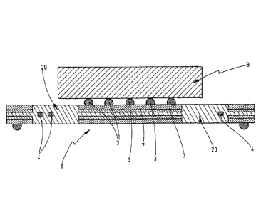
Figure 1 shows a schematic view of a conductor path structure 1, which
comprises
an electronic and/or electromechanical, in particular a micromechanical
component
B, such as an acceleration sensor or the like. The component B is arranged on
a
connection area 2 of the conductor path structure 1, which is designed here as
a so-
called rewiring carrier for the component B. The connection area 2 is arranged
in a
vibration-decoupled manner relative to the area of the conductor path
structure 1
surrounding it, so that an intrinsic damping is formed. It is to be noted that
here as
well as in the following the term "vibration-decoupled" or a synonymous
expression
does not only refer to a complete decoupling, but is also to be understood to
mean a
partial decoupling of oscillations and/or vibrations in the sense of a
damping.
The component B is electrically connected to conductor tracks 4 of the
conductor
path structure 1 by connection elements 3, wherein ¨ as shown in Figure 1 ¨ by
means of these connection elements 3 a distance between the component B and
the
surface of the connection area 2 of the conductor path structure 1 is formed.
A damping device 20 is arranged between the connection area 2 carrying the
component B and the remaining part of the conductor path structure 1.
Exemplary
embodiments of such a damping device are described in the following exemplary
embodiments. In the embodiments shown, the damping device 20 is formed by at
CA 03001497 2018-04-10
- 5 -
least one oscillation- and/or vibration-damping material layer, in particular
an
adhesive layer.
Figures 2 and 3 show a first exemplary embodiment of a conductor path
structure 1
having an intrinsic damping device 20. For the sake of an easier
representation, the
component shown in Figure 1 have been omitted in the aforementioned Figures as
well as in the following Figures. Figure 2 thus shows a top view of the
conductor path
structure 1 and Figure 3 shows an enlarged representation of a section along
the line
A-A of Figure 2. For the sake of better orientation, Figure 2 shows the
section of
Figure 3 on the right top to scale, so that the spatial positional
relationship between
the structures visible in Figure 3 and those of Figure 2 can be seen.
Figures 2 and 3 show the connection area 2 carrying the component B ¨ not
shown
in these Figures ¨ which is provided with the aforementioned connection
elements 3
for the component B. These are connected with the conductor path structure 1
via
conductor paths 4 having contact elements 5, which are arranged in the border
area
6 of the conductor path structure 1. Such a design of a conductor path
structure 1 is
known and hence needs not to be described further.
The structure of the conductor path structure 1 is best seen from Figure 3 in
more
details, which ¨ as described above ¨ represents a sectional view along the
line A-A
of Figure 2. In particular, the conductor tracks 4a and 4b of Figure 2 and the
border
area 6 of the conductor path structure 1 and the connection area 2 for the
component
B can be seen here.
The conductor path structure 1 has a lower base body 10 made of a suitable
carrier
material 11, in particular a laminate. Furthermore, a layer 21 made of a
damping
material, in particular of a damping adhesive, is arranged above it, which
functions as
the intrinsic damping device 20 of the conductor path structure 1.
On the layer 21 the conductor tracks 4, consequently the conductor tracks 4a
and 4b
too, are arranged. Above that plane receiving the conductor tracks 4, 4a, 4b
of the
conductor path structure 1 an upper base body 10' is arranged, which is formed
by a
carrier material 11', in particular a laminate, and which carries on its
underside a
layer of a rigid adhesive 31. In Figure 3 ¨ according to the section along the
line A-A
of Figure 3 ¨ the border area 6 as well as a part of the connection area 2 is
shown. In
CA 03001497 2018-04-10
- 6 -
this case too, the upper base body 10' is formed by a carrier material 11', in
particular
a laminate. Below thereof a layer 31 of a rigid adhesive is arranged.
The rigid adhesive layer 31 serves to stabilize the conductor path structure 1
and to
provide a sufficient connection between corresponding areas of the carrier
material
11' of the base body 10' and the layer 21 formed by the damping material. The
person skilled in the art is aware that this layer 31 made of rigid adhesive
can be
omitted, when the adhesive properties of the material forming the layer 21
allows a
connection between the printed circuit board areas 2a, 6 and that adhesive.
As can best be seen from Figure 3, a free space 7 is provided between the
border
area 6 and the connection area 2, so that there is no mechanical connection
between
this border area 6 and the connection area 2. The connection area 2 is thus
mounted
on the damping layer 21 capable of oscillation and/or vibration. This has the
consequence that oscillations and/or vibrations impinging on the conductor
path
structure 1 are transmitted to the connection area 2 not or only in a damped
manner.
In order to produce the conductor path structure 1 shown in Figures 2 and 3,
firstly
the damping layer 21 of the intrinsic damping device 20 is applied to the
carrier
material 11. Then a lead frame containing conductor tracks 4, 4a, 4b, is
applied onto
said layer 21. Then the carrier material forming the border area 6 and the
connection
area 2 is applied, if necessary with the layer 31 made of a rigid adhesive
arranged on
its underside. However, it is also possible that firstly a partial structure
of the lead
frame structure 1, comprising the carrier material 11, the layer 21 and the
conductor
tracks 4, 4a, 4b, is applied on the layer 31 of a rigid adhesive and then on
this layer
31 the carrier material 11 of the border area 6 as well as the one of the
connection
area 2 are applied. Of course, it is also possible to "reverse" the afore-
described
manufacturing of the conductor path structure 1, i. e. in the representation
of Figures
2 and 3, to start from top, to form the border area 6 and the connection area
2 first
and to apply the further structural components of the conductor path structure
1 as
described before, but in a "reversed order".
The described design of the conductor path structure 1 is characterized by the
fact
that it is no longer necessary to cut out individual areas of a carrier body
and to
provide a resilient device acting as a damping device between them, as is the
case of
the known design. The conductor path structure 1 described is thus
distinguished by
its simple and thus cost-effective producibility and a low build-up height.
CA 03001497 2018-04-10
- 7 -
Figures 4 and 5 show a second exemplary embodiment of such a conductor path
structure 1, wherein corresponding components are provided with the same
reference symbols and are no longer described in more detail. The layered
structure
of the conductor path structure 1 of Figure 4 in turn can be seen in the
sectional view
of Figure 5. The essential difference between the first and second exemplary
embodiments is now, as it also can also be seen from the top view of Figure 4,
the
conductor path structure 1 of the second exemplary embodiment has a closed
surface la. This can also be seen therefrom, that in Figure 4 ¨ in contrast to
Figure 2
¨ the conductor tracks 4, 4a, 4b are ¨ since not visible ¨ shown in dashed
lines. From
Figure 5, it can be seen again, that the conductor path structure 1 has a
lower base
body 10 made of an appropriate carrier material 1, in particular a laminate,
above
which the layer 21, which acts as an intrinsic damping device 20, made of a
damping
material, in particular an adhesive is arranged. The latter carries the
conductor tracks
4, 4a, 4b. Above the conductor tracks 4, 4a, 4b a further layer 22 made of a
damping
adhesive, is arranged, so that the damping device 20, in the embodiment
described
here, comprises the layers 21 and 22, which are each formed by a damping
material,
in particular an adhesive. The conductor tracks 4, 4a, 4b are thus embedded
between these two layers 21 and 22. Above the layer 22, in turn, an upper base
body
10' corresponding to the lower base body 10, formed by an appropriate carrier
material 11', in particular a laminate, is provided.
The manufacturing of the conductor path structure 1 is in turn carried out in
accordance with the first exemplary embodiment, so that it does not have to be
described in detail: The layer 21 of the damping adhesive is applied onto the
carrier
material 1 of the lower base body 10. The conductor tracks 4, 4a, 4b are then
arranged thereon. The layer 22 made of a damping material is applied and
subsequently the carrier material 11' of the upper main body 10'. Of course,
it can be
provided that in the second exemplary embodiment, layers not shown in the
Figures,
corresponding to the layers 31 of the first exemplary embodiment carrier
material 11
and the layer 21 and/or between the layer 22 and the carrier material 11' of
the upper
main body 10' can be provided.
Figures 6 and 7 now show a third exemplary embodiment of a conductor structure
1,
wherein corresponding components are again provided with the same reference
symbols and are no longer described in more detail. The third exemplary
embodiment corresponds in its basic design to the first exemplary embodiment.
It can
CA 03001497 2018-04-10
- 8 -
be seen from the top view of Figure 6, 4a, 4b that the conductor tracks 4, 4a,
4b are
arranged exposedly.
The base body 10' of the third exemplary embodiment corresponds in its
structure to
the base body 10' of the first exemplary embodiment, so that the layer 31 made
of a
rigid adhesive is arranged under the upper layer made of a suitable carrier
material
11', which is forming the cover layer of the conductor path structure 1. The
conductor
tracks 4, 4a are arranged below said layer 31, 4b, thus "hanging" under the
layer 31.
The layer 21 of the damping material is then applied onto the layer 31 of the
base
body 10', which forms the intrinsic damping device 20. These measures allow to
form
the layer 21, which in this embodiment provides the intrinsic damping device
20,
extending over a large area, onto the base body 10 of the conductor path
structure 1
for example by a dispensing process. This simplifies the production of such a
conductor path structure 1 with an intrinsic damping device 20.
In the third exemplary embodiment of Figures 6 and 7, it is now again
provided, that
between the layer 21 and the carrier material 11' of the base body 10' ¨ a
layer 31
made of a rigid adhesive is provided. In this case it is once more true that
this layer
31 serving for reinforcing the conductor path structure 1 can be omitted if
for forming
the layer 31 a damping adhesive is used, which has got sufficiently great
adhesion
properties in order to achieve a reliable connection with the material of the
base body
10.
The production of the conductor path structure 1 is carried out in a manner
that firstly
the upper main body 10' with the carrier material 11' and the layer of rigid
adhesive
31 is formed, and then, on this layer 31 of rigid adhesive, the conductor
tracks 4, 4a,
4b are arranged. The layer 21 of damping material in particular of a damping
adhesive, is then applied over a large area.
In Figures 8 and 9, a fourth exemplary embodiment of a conductor path
structure 1 is
shown, whereby once more components corresponding to one another are provided
with the same reference symbols and are no longer described further.
The fourth exemplary embodiment corresponds to the third exemplary embodiment,
with the provision that the layer 21 made of damping material, in particular
made of
an adhesive, is applied ¨ as in the third exemplary embodiment ¨ over a large
area,
CA 03001497 2018-04-10
- 9 -
but in the configuration of local pads ("pads") 21' made of a damping
material, in
particular of an adhesive.
To this end, it is provided that the carrier material 11 of the lower base
body 10 of the
conductor path structure 1 has at least one recess 12, into which the
aforementioned
local pads 21' are then arranged. This can be achieved by inserting already
prefabricated local pads or by locally applying the layer 21 of the damping
material.
Alternatively, it is possible that the upper base body 10', instead of the
lower basic
body 10, has at least one such recess 12, into which the aforementioned local
pad
21' is then arranged. The lower base body 10 can then optionally be omitted.
Of
course, a combination of these measures is also possible, that both the base
body 10
and the base body 10' have at least one corresponding recess 12.
A fifth exemplary embodiment of the conductor path structure 1 is shown in
Figures
and 11, wherein once more corresponding components are provided with the
same reference symbols and are no longer described further. The structure of
the
fifth exemplary embodiment essentially corresponds to the one of the fourth
exemplary embodiment, the conductor path structure 1 thus has a closed surface
1',
as it can be seen from the dashed-line representation of the conductor tracks
4, 4a,
4b. The lower base body 10 and the upper base body 10' each have a recess 12
and
12' respectively, which ¨ as can best be seen from Figure 11 ¨ are filled by a
layer of
damping material 21, in particular of a damping adhesive. The essential
difference
between the fourth and fifth exemplary embodiments is thus, that in the latter
embodiment, instead of locally applied damping pads 21' a damping material, in
particular a damping adhesive, is injected, printed or dispensed.
The conductor path structure 1 of the fifth exemplary embodiment is produced
by
means of a standard lamination technique. The conductor tracks 4, 4a, 4b and
carrier
films with adhesive layers are placed in a corresponding injection moulding
tool. In
the closed injection moulding tool, the shaping cavity in the area of the
exposed
conductor tracks in the area of the free space 7 is filled with damping
material, which
forms the layer 21. The lamination of the carrier layers onto the conductor
tracks 4,
4a, 4b can be carried out either as a process upstream of the aforementioned
injection moulding process as well as during the injection moulding process in
the
injection moulding tool.
CA 03001497 2018-04-10
- 10
In summary, it is to be stated that, by means of the described measures, a
conductor
path structure 1 comprising an intrinsic damping device 20 is provided, which
is
distinguished by its simple and thus cost-effective producibility. It is now
not required
any longer that, for forming the intrinsic damping device 20, to cut-out
respective
sections of the lower base body 10 and/or the upper base body 10', which are
then
connected by an elastically resilient device for forming the oscillation
and/or vibration
damped connection area 2. Rather, it is provided that the intrinsic damping
device 20
is formed by one or more layers 21, 22 made of a damping material, in
particular a
damping adhesive. Such a measure has the further advantage, that the conductor
path structure 1 provided with the described damping device 20 is
distinguished by a
low overall height.