Note: Descriptions are shown in the official language in which they were submitted.
CA 03002318 2018-04-17
WO 2016/207660
PCT/GB2016/051909
1
Method of, and apparatus for, reducing photoelectron yield and/or secondary
electron yield
The present invention relates to methods of treating surfaces in order to
reduce
photoelectron yield (PEY) and/or secondary electron yield (SEY).
BACKGROUND
Photoelectron emission (PEE) refers to the emission of electrons due to
interaction of
photons with a surface. Secondary electron emission (SEE) refers to emission
of a
secondary electron from a surface due to interaction of a primary electron
with the
surface. Photoelectron yield (REV) can be used to characterise PEE and
secondary
electron yield (SEY) can be used to characterise SEE. PEY and SEY may be taken
to
be the average number of emitted electrons per single incident photon or
electron
respectively.
PEE and SEE effects can cause significant difficulties in a wide variety of
apparatus, for
example in particle accelerators, beamlines, waveguides, for example r.f.
waveguides,
detectors, spacecraft, and vacuum chambers. PEE and SEE effects can lead,
variously,
to undesired electron cloud build-up, undesired increases in pressure, beam
losses and
instability, reduction in beam lifetimes, undesired heat loads, power loss,
damage,
reduction in apparatus lifetime, increase in noise, and decrease in
sensitivity, depending
on the particular type of apparatus and application in question.
It is desired to provide improved or at least alternative methods for reducing
PEY and
SEY.
SUMMARY
In a first aspect of the invention there is provided a method of reducing
photoelectron
yield (PEY) and/or secondary electron yield (SEY) of a surface, comprising:
applying laser radiation to the surface to produce a periodic arrangement of
structures on the surface, wherein
CA 03002318 2018-04-17
WO 2016/207660
PCT/GB2016/051909
2
the laser radiation comprises pulsed laser radiation comprising a series of
laser
pulses and the power density of the pulses is in a range 0.01 TW/cm2 to 3
TW/cm2,
optionally 0.1 TW/cm2 to 3 1W/cm2.
Optionally the power density may be in a range 0.1 1W/cm2 to 2 1W/cm2,
optionally in a
range 0.3 1W/cm2 to 2 1W/cm2, optionally in a range 0.4 TW/cm2 to 1.5 TW/cm2,
further
optionally in a range 0.38 1W/cnn2 to 0.6 TW/cm2, 0.16 TW/cm2 to 0.54 TW/cm2.
By using laser pulses having such power densities, a periodic arrangement of
structures
that provides a surface with desired properties may be obtained. For example a
surface
having a desired value or range of values of secondary electron yield (SEY)
may be
obtained.
The method may alter the properties of surface such that the surface has a
value of SEY
less than 1.5, optionally less than 1.2, optionally less than 1.0, optionally
less than or
equal to 0.7, optionally in a range 0.2 to 1.0, optionally in a range 0.5 to
1.0, optionally in
a range 0.3 to 0.9, optionally in a range 0.6 to 0.8, optionally approximately
equal to 0.7.
The values of SEY may be values immediately after applying of the laser
radiation, for
example before any build-up of grease, dirt, oxides or other contirninants or
extraneous
materials, and/or after cleaning.
The laser pulses may have a duration less than a thermal relaxation time of
the material
of the surface. The laser pulses may have a duration such that the electrons
and the
atomic lattice of the material of the surface have a substantially different
temperature
substantially throughout application of the laser pulses. The laser pulses may
have a
duration such that material of the surface is at least one of evaporated or
vaporised or
removed without substantial melting and/or flowing of the surface. The laser
pulses may
have a duration such that some material of the surface is at least one of
evaporated or
vaporised or removed without substantial melting and/or flowing of the
remaining
material of the surface.
A pulse duration of the laser pulses may be in a range 200 femtoseconds (fs)
to 1000
picoseconds (ps).
CA 03002318 2018-04-17
WO 2016/207660
PCT/GB2016/051909
3
The periodic arrangement of structures on the surface may comprise a periodic
series of
peaks and troughs substantially parallel to each other, and the peaks may be
substantially flat on top and/or may be rounded on top and/or may have
substantially no
pointed and/or or sharp regions on top. The peaks may substantially have a top
hat
shape and/or a truncated pyramidal shape, for example a top hat shape and/or a
truncated pyramidal shape in cross-sectional profile. Thus, for example, a
desired value
of electron work function and/or desired electron trapping properties may be
obtained.
The peaks may extend in a longitudinal direction and may be referred to as
ridges.
The peak to trough distance for at least some of the peaks, and/or an average
or median
peak to trough distance, may be in a range 500 nm to 100 pm , optionally 5 pm
to 100
pm, optionally in a range 20 pm to 80 pm, optionally in a range 1 pm to 60 pm,
optionally
in a range 30 pm to 60 pm.
The periodic arrangement of structures may comprise a cross-hatched
arrangement or
an arrangement of substantially parallel lines of peaks and troughs (for
example, ridges
and valleys) substantially without cross-hatching. The periodic arrangement
of
structures may, for example, be produced by a single pass of a laser source
that
provided the laser radiation.
The surface may be on an at least one underlying layer (for example, at least
one of
steel, stainless steel) and the laser radiation may be such as to
substantially not remove
or move material of the surface in such a way as to expose the underlying
layer.
The method may further comprise at least one of degreasing, cleaning or
smoothing said
surface after the applying of the laser radiation, and/or performing a surface
carbon
reduction process with respect to said surface after the applying of the laser
radiation.
In a further aspect of the invention, which may be provided independently,
there is
provided a method of reducing photoelectron yield (PEY) and/or secondary
electron
yield (SEY) of a surface, comprising:
applying laser radiation to the surface to produce a periodic arrangement of
structures on the surface, wherein the laser radiation comprises pulsed laser
radiation
comprising a series of laser pulses; and
CA 03002318 2018-04-17
WO 2016/207660
PCT/GB2016/051909
4
at least one of degreasing, cleaning or smoothing said surface after the
applying
of the laser radiation, and/or performing a surface carbon reduction process
with respect
to said surface after the applying of the laser radiation.
The cleaning may comprise performing a chemical cleaning process or using an
extraction unit, for example a process to remove materials adhered to or
otherwise
present at or in the surface, for example by way of dissolving, flushing,
scouring and/or
reacting with such materials, or by using an inert gas (for example nitrogen)
blower,
pressure cleaner or air gun.
In a further aspect of the invention, which may be provided independently,
there is
provided a laser treated surface comprising a laser-formed periodic
arrangement of
structures on the surface, wherein at least one of:
the periodic arrangement of structures comprises a periodic series of peaks
and
troughs substantially parallel to each other;
the periodic arrangement of structures comprises a cross-hatched, periodic
series of peaks and troughs; and optionally
the peaks may be substantially flat on top and/or may be rounded on top and/or
may have substantially no pointed and/or or sharp regions on top and/or the
peaks may
substantially have a top hat shape and/or a truncated pyramidal shape, for
example a
top hat shape and/or a truncated pyramidal shape in cross-sectional profile;
and/or
the peak to trough distance for at least some of the peaks, and/or an average
or
median peak to trough distance, may be in a range 500 nm to 100 pm, optionally
in a
range 5 pm to 100 pm, optionally in a range 20 pm to 80 pm, optionally in a
range 1 pm
to 60 pm, optionally in a range 30 pm to 60 pm.
In a further aspect of the invention, which may be provided independently,
there is
provided an apparatus for reducing photoelectron yield (PEY) and/or secondary
electron
yield (SEY) of a surface, comprising:
a laser source for applying pulsed laser radiation to a surface; and
a laser controller configured to control the laser source to apply the laser
radiation as a series of laser pulses thereby to form a periodic arrangement
of structures
on the surface, wherein the power density of the pulses is in a range 0.01
TW/cm2 to 3
TW/cm2, optionally 0.1 TW/cm2 to 3 TW/cm2.
CA 03002318 2018-04-17
WO 2016/207660
PCT/GB2016/051909
In a further aspect of the invention, there is provided a method of reducing
photoelectron
yield (PEY) and/or secondary electron yield (SEY) of a surface, comprising:
applying laser radiation to the surface to produce a periodic arrangement of
structures on the surface, wherein
the laser radiation comprises pulsed laser radiation comprising a series of
laser
pulses, and a pulse duration of the laser pulses is in a range 200
femtoseconds (fs) to
1000 picoseconds (ps).
The surface may be the surface of a target.
The pulse duration may be in a range 1 ps to 100 ps. The pulse duration may be
in a
range 1 ps to 50 ps. The pulse duration may be in a range 5ps to 500 ps
The laser radiation may comprise a pulsed laser beam that has a focal spot
diameter on
the surface in a range 1 jim to 50 vim or in a range 1 p.m to 100 [tin.
The pulsed radiation may have a pulse repetition rate in a range 10 kHz to 1
MHz.
An average power of the laser radiation may be in a range 0.3 W to 20W,
optionally in a
range 0.3 W to 2W, or in a range 1 W to 10W, or in a range 1 W to 5W, or in a
range
0.1 W to 1W, or in a range 0.1 W to 2W, or in a range 0.3W to 5W.
The applying of the laser radiation to the surface may comprise scanning a
pulsed laser
beam over the surface, and a scan speed for the scanning may be in a range 1
mm/s to
200 mm/s, optionally in a range 1 mm/s to 100 mm/s.
The scanning of the pulsed laser beam over the surface may be repeated between
2
and 10 times, or may be performed once.
An angle of incidence of the laser radiation to the surface may be in a range
from 0 to 30
degrees. The angle of incidence of the laser radiation to the surface may be
in a range
from 90 degree to 60 degrees.
A wavelength of the radiation may be in a range 100 nm to 2,000 nm, optionally
532 nm
or 528 nm or 1030 nm or 1064 nm or 1070 nm.
CA 03002318 2018-04-17
WO 2016/207660
PCT/GB2016/051909
6
The structures may comprise peaks and troughs. The periodic arrangement of
structures may comprise a periodic series of peaks and troughs. The peaks and
troughs
may be substantially parallel to each other.
The periodic arrangement of structures may comprise a first series of peaks
and troughs
arranged in a first direction, and a second series of peaks and troughs
arranged in a
second, different direction. The first and second directions may be
substantially
orthogonal. The first series of peaks and troughs and the second series of
peaks and
troughs may intersect such that the periodic arrangement of structures
comprises a
cross-hatched arrangement.
A period of the periodic arrangement may be in a range 0.5 pm to 100 pm. The
separation of adjacent peaks (or troughs) of the periodic structure may be in
a range 0.5
pm to 100 pm. A hatch distance of the cross-hatched arrangement may be in a
range
0.5 pm to 100 pm.
The laser radiation may be such that the applying of the laser radiation to
the surface
comprises producing further structures. The further structures may be smaller
than the
structures of the periodic arrangement of structures.
That feature may be particularly important, so in a further aspect of the
invention, which
may be provided independently, there is provided a method of reducing
photoelectron
yield (PEY) and/or secondary electron yield (SEY) of a surface, comprising:
applying laser radiation to the surface to produce a periodic arrangement of
structures on the surface, wherein
the laser radiation comprises pulsed laser radiation comprising a series of
laser
pulses, and the laser radiation is such as to produce further structures on
the surface as
well as the periodic arrangement of structures.
The further structures may comprise further periodic structures. The further
structures
may comprise ripples. The further structures may comprise nano-ripples. The
further
structures may be further periodic structures. The further structures may
comprise laser
induced periodic surface structures (LIPPS). The further structures may
have a
periodicity in a range 10 nm to 1 prn, optionally in a range 100 nm to 1 pm.
CA 03002318 2018-04-17
WO 2016/207660
PCT/GB2016/051909
7
The further structures may cover at least part of the periodic array of
structures. The
further structures may be formed in the troughs and/or on the peaks of the
periodic
arrangement of structures.
The surface may be a metal surface. The surface and/or target may comprise
copper,
aluminium, stainless steel or titanium. The metal of the metal surface may be
a metal
selected from copper, aluminium, stainless steel, or titanium. The surface may
form part
of a laminated structure, for example a laminated target, for instance
comprising one of
copper, aluminium, stainless steel, titanium and at least one other material,
and/or a
laminated structure comprising at least two of copper, aluminium, stainless
steel,
titanium.
The surface may be the surface of a foil. The target may be a foil.
An average or peak fluence or other property of the laser radiation may be
above an
ablation threshold of the surface and within 105%, optionally 102%, optionally
101% of
the ablation threshold.
The pulses may be such that, for each pulse, a plasma is formed at the
surface. The
plasma may have substantially the same density as underlying material of the
surface.
The surface may form part of a particle accelerator, a beamline, a waveguide
for
example an r.f. waveguide, a detector, a detector apparatus, or a spacecraft.
The surface may comprise or form part of a surface of a vacuum chamber.
The surface may comprise a surface of a component of an apparatus. The
apparatus
may be selected from: a particle accelerator, a beamline, a waveguide for
example an
r.f. waveguide, a detector, a detector apparatus, a spacecraft. The method may
comprise applying the laser radiation to the surface to produce the periodic
arrangement
of structures on the surface and then installing the component in the
apparatus, or the
method may comprise applying the laser radiation to the surface with the
component in
situ in the apparatus.
CA 03002318 2018-04-17
WO 2016/207660
PCT/GB2016/051909
8
The method may comprise applying the radiation using a solid-state laser,
optionally the
solid state laser comprises a Nd:YV04 or Nd:YAG or Yb:YAG or Nd:KGW or Nd:KYW
or
Yb:KGW or Yb:KYW laser, or a pulsed fibre laser, optionally a Yb, Tm or Nd
pulsed fibre
laser. The applied radiation may comprise the fundamental wavelengths of
operation
such lasers or their second or third harmonics.
In a further aspect of the invention, which may be provided independently,
there is
provided an apparatus for reducing photoelectron yield (PEY) and/or secondary
electron
yield (SEY) of a surface, comprising:
a laser source for applying pulsed laser radiation to a surface; and
a laser controller configured to control the laser source to apply the laser
radiation as a series of laser pulses having a pulse duration in a range 200
femtoseconds (fs) to 1000 Ps, so to produce a periodic arrangement of
structures on the
surface.
In a further aspect of the invention, which may be provided independently,
there is
provided an apparatus for reducing photoelectron yield (PEY) and/or secondary
electron
yield (SEY) of a surface, comprising:
a laser source for applying pulsed laser radiation to a surface and configured
to
operate so as to perform a method according to any other aspect.
In a further aspect of the invention, which may be provided independently
there is
provided a laser treated surface comprising a periodic arrangement of
structures on the
surface formed using a method according to any other aspect.
In a further aspect of the invention, which may be provided independently,
there is
provided a laser treated surface comprising a laser-formed periodic
arrangement of
structures on the surface and further laser-formed structures on the surface.
The further structures may comprise further periodic structures. The further
structures
may comprise ripples. The further structures may comprise nano-ripples. The
further
structures may be further periodic structures. The further structures may
comprise laser
induced periodic surface structures (LIPPS). The further structures may
have a
periodicity in a range 10 nm to 1 p.m, optionally in a range 100 nm to 1
t.t.m.
CA 03002318 2018-04-17
WO 2016/207660
PCT/GB2016/051909
9
The structures may comprise peaks and troughs. The periodic arrangement of
structures may comprise a periodic series of peaks and troughs. The peaks and
troughs
may be substantially parallel to each other.
The periodic arrangement of structures may comprise a first series of peaks
and troughs
arranged in a first direction, and a second series of peaks and troughs
arranged in a
second, different direction. The first and second directions may be
substantially
orthogonal. The first series of peaks and troughs and the second series of
peaks and
troughs may intersect such that the periodic arrangement of structures
comprises a
cross-hatched arrangement.
A period of the periodic arrangement may be in a range 0,5 pm to 100 pm. The
separation of adjacent peaks (or troughs) of the periodic structure may be in
a range 0.5
p.m to 100 pm. A hatch distance of the cross-hatched arrangement may be in a
range
0.5 pm to 100 pm.
The further structures may comprise further periodic structures. The further
structures
may comprise ripples. The further structures may comprise nano-ripples. The
further
structures may be further periodic structures. The further structures may
comprise laser
induced periodic surface structures (LIPPS). The
further structures may have a
periodicity in a range 10 nm to 1 pm, optionally in a range 100 nm to 1 pm.
The further structures may cover at least part of the periodic array of
structures. The
further structures may be formed in the troughs of the periodic arrangement of
structures.
The surface may be a metal surface. The surface may comprise copper,
aluminium,
stainless steel or titanium. The metal
of the metal surface may be selected from
copper, aluminium, stainless steel, titanium. The surface may form part of a
laminated
structure, for example a laminated target, for instance comprising one of
copper,
aluminium, stainless steel, titanium and at least one other material, and/or a
laminated
structure comprising at least two of copper, aluminium, stainless steel,
titanium.
In a further aspect of the invention, which may be provided independently,
there is
provided a particle accelerator, a beamline, a waveguide, a detector, a
spacecraft, or a
CA 03002318 2018-04-17
WO 2016/207660
PCT/GB2016/051909
vacuum chamber that includes a component having a surface according to the
fifth
aspect or the sixth aspect of the invention.
In further aspects of the invention there are provided a method, a surface, a
structure
comprising a surface, an apparatus, a component, a particle accelerator, a
beamline, a
waveguide, a detector, a spacecraft, or a vacuum chamber as described and/or
illustrated herein.
Any feature in any one or more of the aspects of the invention may be applied
to any
other one or more of the aspects of the invention in any appropriate
combination.
BRIEF DESCRIPTION OF THE DRAWINGS
Embodiments of the invention are further described hereinafter with reference
to
the accompanying drawings, in which:
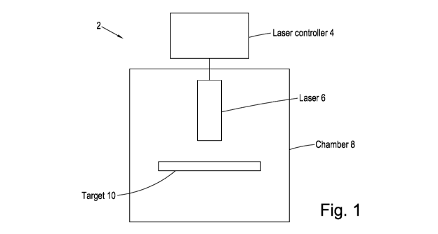
Figure 1 is a schematic diagram of a system used for laser treatment of a
surface
to reduce photoelectron emission (PEE) and/or secondary electron emission
(SEE)
effects, for example to reduce photoelectron yield (PEY) and/or secondary
photoelectron
yield (SEY);
Figure 2 shows images of copper samples following laser treatment to form
periodic structures on the surfaces of the samples;
Figure 3 shows images of aluminium samples following laser treatment to form
periodic structures on the surfaces of the samples;
Figures 4a and 4b show images of aluminium samples following laser treatment
to form periodic structures on the surfaces of the samples; and
Figure 5 to 24 show images of further samples and/or plots of properties of
further samples, following laser treatment to form periodic structures on the
surfaces of
the further samples;
Figure 25 shows images of two samples before performance of measurements
as outlined in Appendix 1;
Figure 26 and 27 are plots of SEY as a function of primary energy for the
samples of Figure 25;
Figures 28a and 28b show images of samples before and after degreasing as
described in Appendix 3;
CA 03002318 2018-04-17
WO 2016/207660
PCT/GB2016/051909
11
Figures 29 to 32 are plots of measurements performed on samples before and
after storage and/or degreasing, as described in Appendix 3;
Figure 33 shows images of samples that are the subject of Appendix 4;
Figure 34 shows optical microscope images of samples that are the subject of
Appendix 4;
Figures 35 and 36 show SEM images of samples that are the subject of
Appendix 4; and
Figures 37a and 37b are schematic illustrations of laser interaction
mechanisms.
DETAILED DESCRIPTION
Figure 1 shows a system used for laser treatment of a surface to reduce
photoelectron
emission (PEE) and/or secondary electron emission (SEE) effects, for example
to
reduce photoelectron yield (PEY) and/or secondary electron yield (SEY).
The system 2 of Figure 1 comprises a laser 6 connected to a laser controller 6
which is
used to control operation of the laser 6 to emit a pulsed laser radiation beam
of desired
characteristics. The laser 6 is aligned with a target 10 such that operation
of the laser 6
under control of the laser controller 4 forms periodic structures on the
surface of the
target.
In embodiments, the laser may be one of a Nd:YV04 or Nd:YAG laser, or a pulsed
fibre
laser, for example a Yb, Tm or Nd pulsed fibre laser. Any other suitable laser
may be
used in alternative embodiments. In the embodiment of Figure 1, the wavelength
of the
pulsed laser radiation is 532 nm, but any other suitable wavelength can be
used in other
embodiments, for example 628 nm or 1030 nm or 1064 nm or 1070 nm.
The controller may comprise a dedicated controller, or a suitably programmed
computer.
The controller may be implemented in software, hardware or any suitable
combination of
hardware and software. In some embodiments, the controller may comprise more
ASICs
(application specific integrated circuits) or FPGAs (field programmable gate
arrays) or
other suitable circuitry.
CA 03002318 2018-04-17
WO 2016/207660
PCT/GB2016/051909
12
In the embodiment of Figure 1, the target 10 and laser 6 are located in air
and the laser
treatment of the surface is performed in air. The target 10 and laser 6 may be
positioned
in a sealable and/or pumpable chamber 8 that has an associated pump and/or gas
supply, and the laser processing of the surface may be performed in vacuum or
in
desired gaseous conditions, for example in the presence of a selected reactive
gas. The
chamber 8 is omitted in some embodiments.
In the embodiment of Figure 1, the target 10 is a metal target comprising
copper. Other
targets, for example aluminium, stainless steel or titanium can be used.
In operation pulsed laser radiation of desired characteristics is scanned
across the
surface of the target 10 by the laser 6 under control of the laser controller
4 to produce a
periodic arrangement of structures on the surface. For example, in order to
form peaks
and troughs arranged in parallel rows, the laser beam may be scanned along
parallel,
spaced-apart paths across the surface to form parallel troughs separated by
peaks. Any
other suitable arrangements of structures can be formed by suitable scanning
of the
laser beam over the surface.
Operating parameters of the laser, and certain equations linking such
parameters, can
be represented as follows,
Wavelength (A) [m]
Repetition rate of the laser (y) [Hz]
Pulse length of the laser (T) [s]
Average power of the laser (Pavg) [W] ¨ represents the energy flow over one
period t
Energy per pulse (Ep) [J]
Fluence of the laser (F) [J/cm2]
Beam spot radius on the target (r) [m]
Beam spot area on the target (A-.4-11T2)[m2i
Number of times surface of the target was scanned by the laser beam (N)
dimensionless
Speed at which surface of the target was scanned by the laser beam (V) [m/s]
CA 03002318 2018-04-17
WO 2016/207660 PCT/GB2016/051909
13
Number of pulses fired per each spot on the surface of the target (n)
[dimensionless]
Time interval between the pulses ¨ one period (t) [s]
Peak Power (Ppeak) [W] ¨ defines the energy flow within a single pulse
Power density or Intensity (I) [W/crn2]
Equations
t= -1
(20y
n = __
V
Pavg
E
P y
Epulse
F =
A
Epulse
Ppeak = T
Ppeak
I
A
Suitable operating parameters can be selected, for example based on the
equations and
representations above, to obtain pulsed laser radiation of desired properties,
for example
a desired power density of the pulses.
Table 1 provides operating parameters of the laser to produce a desired
periodic
arrangement of structures on the surface, for an embodiment where the surface
is
copper. Three sets of operating parameters according to an embodiment are
provided
in table 1. The laser processing of the surface is performed in air in this
case.
Copper
Wavelength Pulse Focal Rep. Average Scan Re petitio Hatch
Fluence,
Widt Spot Rate Power, Speed n Number
Distance J/cm2
rim h Diamete of of the (Numbe
CA 03002318 2018-04-17
WO 2016/207660
PCT/GB2016/051909
14
Rang ran the the mm/s scans Vim r of
target, laser pulses
!Ann per
kHz spot)
532*** ¨10ps 12 200 0.94 10 1 24 4.16
(range (240)
betwee
n 0.77
to 1.00)
532** ¨10ps 40 200 0.75 10 1 30 0.3
(800)
1064* ¨10ps 73 200 3.27 30 1 - 55 0.39
(487)
Table 1
*- SEY data on the structuring is 1.8 and 1.6 for linear- and cross-hatched
scans
respectively; possible reason is REDUCED SURFACE TOPOGRAPHY compare to
532nm processing, SEM images available.
SEY data on the structuring is 1.13 (DL) and 1.3 (CERN). Processing parameters
used for the first batch of CERN samples (Cu OFE and co-laminated Cu (layer
thickness
is ¨80pm) on Stainless Steel).
***- REPORTED SEY data on the structuring: 0.75 (DL) and 0.95 (CERN).
In some other embodiments where the target is copper, operating parameters are
selected as follows:
a) Wavelength of 532 nm; Pulse width of the laser: from 200 femtosecond to 200
picosecond; Focal spot diameter on the target: from 1 pm to 50 pm; Repetition
rate of the laser from 10 kHz to 1 MHz; Average power from 0.3 W to 2W; Scan
speeds of 1 mm/s to 100 mm/s; Repetition number of scans from 1 to 10; Hatch
Distance from 0.5 pm to 100 pm; angle of incidence of the laser beam from 0 to
30 degrees.
b) Wavelength of 1064 nnn; Pulse width of the laser: from 200 femtosecond to
200
picosecond; Focal spot diameter on the target: from 1 pm to 50 pm; Repetition
rate of the laser from 10 kHz to 1 MHz; Average power from 1 W to 5 W; Scan
speeds of 1 mm/s to 100 mm/s; Repetition number of scans from 1 to 10; Hatch
Distance from 0.5 pm to 100 pm; angle of incidence of the laser beam from 0 to
30 degrees.
CA 03002318 2018-04-17
WO 2016/207660 PCT/GB2016/051909
Table 2 provides operating parameters of the laser to produce a desired
periodic
arrangement of structures on the surface, for an embodiment where the surface
is
aluminium.
Aluminium
Wavelength, Pulse Focal Rep. Average Scan Repetition Hatch Fluence,
nrn Width Spot Rate Power, Speed, Number Distance, J/cm2
Range Diameter of W mm/s of the im (Number
on the the scans of pulses
target, laser, per
P.m kHz spot)
1064 ¨10ps 12 200 0.21 10 1 20 0.93
(240)
Table 2
In some other embodiments where the target is aluminium, operating parameters
are
selected as follows:
a) Wavelength of 1064 nm; Pulse width of the laser: from 200 femtosecond to
200
picosecond; Focal spot diameter on the target: from 1 pm to 50 pm; Repetition
rate of the laser from 10 kHz to 1 MHz; Average power from 0.1 W to 1 W; Scan
speeds of 1 mm/s to 100 mm/s; Repetition number of scans from 1 to 10; Hatch
Distance from 0.5 pm to 100 pm; angle of incidence of the laser beam from 0 to
30 degrees.
Table 3 provides operating parameters of the laser to produce a desired
periodic
arrangement of structures on the surface, for an embodiment where the surface
is
stainless steel.
Stainless
steel
Wavelength, Pulse Focal Rep. Average Scan Repetition Hatch Fluence,
nm Width Spot Rate Power, Speed, Number Distance, J/crn2
Range Diameter of W mm/s of the tan (Number
on the the scans of pulses
target, laser, per
jim kHz spot)
CA 03002318 2018-04-17
WO 2016/207660
PCT/GB2016/051909
16
532 ¨10ps 12 200 0.44 10 1 24 1.95
(240)
Table 3
In some other embodiments where the target is stainless steel, operating
parameters are
selected as follows:
a) Wavelength of 532 nm; Pulse width of the laser: from 200 femtosecond to 200
picosecond; Focal spot diameter on the target: from 1 p.m to 50 iim;
Repetition
rate of the laser from 10 kHz to 1 MHz; Average power from 0.1 W to 2 W; Scan
speeds of 1 minis to 100 mm/s; Repetition number of scans from 1 to 10; Hatch
Distance from 0.51.tm to 100 pm.
b) Wavelength of 1064 nm; Pulse width of the laser: from 200 femtosecond to
200
picosecond; Focal spot diameter on the target: from 1 jim to 50 Jim;
Repetition
rate of the laser from 10 kHz to 1 MHz; Average power from 1 W to 5 W; Scan
speeds of 1 mm/s to 100 mm/s; Repetition number of scans from 1 to 10; Hatch
Distance from 0.5 1.tm to 100 vtm; angle of incidence of the laser beam from 0
to
30 degrees.
Figure 2 shows images of copper samples following laser treatment to form
periodic
structures on the surfaces of the samples as described in relation to Figure
1. The
operating parameters used in the laser treatment of the copper samples are
provided in
the following table, Table 4. Three samples were treated, copper samples a),
b) and c).
Images of the samples a), b) and c), and four scanning electron microscope
(SEM)
images of the processed surfaces of samples, labelled 1 to 4, are shown in
Figure 2 and
described in Table 4 below. SEY results for 13 mm copper samples are provided
in
Appendix 1 below.
Figure 3 shows images of aluminium samples following laser treatment to form
periodic
structures on the surface as described in relation to Figure 1. The operating
parameters
used in the laser treatment of the aluminium samples are provided in the
following table,
Table 5. Two samples were treated, aluminium samples a) and b). Images of the
samples a) and b) and three scanning electron microscope (SEM) images of the
processed surface of a sample at different levels of magnification, labelled 1
to 3, are
shown in the figure and described in Table 5 below.
CA 03002318 2018-04-17
WO 2016/207660
PCT/GB2016/051909
17
Samples:
a) Cu OFE disk, 0 29min, thickness 1111111 -processed area of about 0 28mm,
b) Cu OFE disk, 0 13rnm, thickness linun -processed area of about 0 12mm.
e) Cu OFE substrate, 20x20mm, thickness hum -processed area of 15x15unn.
a) lie)
SEMs of the processed areas
1 2
Wavelength := 532 urn; Pulse length 10 ps; Wavelength = 532 mu; Pulse
length 10 ps:
Focal spot diameter on the target= 12 Focal spot diameter on the target =
12
micrometres; Rep. rate of the laser = 200 kHz; micrometres; Rep. rate of the
laser = 200
Average power = 0.81 W; Scan speed = 10 kHz; Average power = 0.95 W; SCAll.
speed =
mints; Single scan over the surface; Hatch 10 nun/s; Single scan over the
surface;
distance between the lines = 24 micrometres: Hatch distance between the
lines = 24
Number of pulses fired per spot = 240 micrometres; Number of pulses fired
per
spot = 240
3 4
Wavelength = 532 nm; Pulse length 10 ps: Wavelength = 532 nun Pulse length
10 ps;
Focal spot diameter on the target = 12 Focal spot diameter on the target =
12
micrometres; Rep. rate of the laser = 200 kHz; micrometres; Rep. rate of
the laser = 200
Average power = 0.77 W; Scan speed = 10 kHz; Average power = 0.90W; Scan
speed =
mints; Single scan over the surface; Hatch 10 mm/s; Single scan over the
surface;
distance between the lines = 24 micrometres: Hatch distance between the
lines = 24
Number of pulses fired per spot = 240 micrometres; Number of pulses fired
per
spot = 240
5, 6, 7, 8,9 and 10 are all the similar 6
parameters but only with different average
powers within the range given in the
parameters data.
7 8
9 10
Table 4
CA 03002318 2018-04-17
WO 2016/207660
PCT/GB2016/051909
18
Samples:
a) Aluminium, 25x25mm, thickness lnun -processed area of about 20x2Omm.
b) Aluminium, thickness imm -processed area of about 5x5min,
a) b)
SEMs of the processed areas
1 2
Wavelength = 1064 nm; Pulse length 10 ps; The same parameters as in image
1. it is a
Focal spot diameter on the target = 12 higher magnification (10000) of the
micrometves; Rep. rate of the laser = 200 kHz; image presented in 1.
Average power = 0.21 W; Scan speed = 10
minis; Single scan over the surface; Hatch
distance between the lines = 20 micrometres;
Number of pulses fired per spot = 240
3
The same as one. it is a higher
magnification (1400) of the image
presented in 1. The parameters are the
same.
Table 5
Figures 4a and 4b shows images of stainless steel samples following laser
treatment to
form periodic structures on the surface as described in relation to Figure 1.
The
operating parameters used in the laser treatment of the samples are provided
in the
following tables, Tables 6a and 6b. Four samples were treated, stainless steel
samples
a), b), c) and d). Images of the samples a), b), e) and d) and scanning
electron
microscope (SEM) images of the processed surfaces of the samples, labelled 1
to 10,
are shown in Figures 4a and 4b and described in Tables 6a and 6b below.
CA 03002318 2018-04-17
WO 2016/207660
PCT/GB2016/051909
19
Samples:
a) Stainless Steel, 20x2Olum, thickness 200pm -processed area of about ii
18min.
h) Stainless Sled, thickness llum -processed area of about 20x2Oinm.
c&d) Stainless Steel (not polished(c), polished (d)). thickness lmm, various
processed
areas.
a) b) c) d)
SEMs of the processed areas
1 2
Wavelength = 532 mrs; Pulse length 10 pa; The same parameters as in image
1. It is a
Focal spot diameter on the target = 12 higher magnification (3000) of the
image
micrometres; Rep. rate of the laser = 200 kHz; presented in 1.
Average power = 0.44W; Scan speed -10
nun/s; Single scan over the surface; Hatch
distance between the lines 24 micrometres;
Number of pulses fired per spot= 240
3 4
The same parameters as in image 1. It is a Wavelength - 1064 nan: Pulse
length 20 ps;
higher magnification (5000) of the image Focal spot diameter on the target
= 15
presented in L micrometres; Rep. rate of the laser= 200
kHz; Average power 0.8W; Scan speed -
minis; Single scan over the surface;
Hatch distance between the lines = 24
micrometres: Number of pulses fired per
spot = 300
5
The same parameters as in image 4. It is a The same parameters as in image
4. It is a
higher magnification (3000) of the image higher magnification (3000) of the
image
presented in 1. presented in 1.
7 3
Example of linear scan, Wavelength = 532 Example of linear scan. Wavelength
= 1064
mu Pulse length 10 ps; Focal spot diameter on urn; Pulse length 20 ps; Focal
spot diameter
the target 12 micrometres: Rep. rate of the on the target = 15 micrometres:
Rep. rate of
laser = 200 Itliz; Average power = 0.44W; Scan the lase-r= 200 kHz: Average
power = 0.8W;
speed .= 10 mm/s; Single scan over the surface; Scan speed = 10 minis; Single
scan over the
Hatch distance between the lines - 24 surface; Hatch distance between the
lines =
micrometres: Humber of pulses fired per spot 24 micrometres; Number of pulses
fired per
=240 spot = 300
Table 6a
9 10
The same parameters as in image 8. It is a The same parameters as in image
8. It is a
higher magnification (3000) of the image higher magnification (3000) of the
image
presented in 1. presented in 1.
Table 6b
CA 03002318 2018-04-17
WO 2016/207660
PCT/GB2016/051909
Appendix 2 provides further operating parameters of the laser to produce a
desired
periodic arrangement of structures on the surface according to further
embodiments.
Figure 5 shows an image of a copper sample following laser treatment to form
periodic
structures (in this case cross-hatched structures) on the surface of the
sample as
described. Five SEM images at five points (labelled 1, 3, 6, 9, 12) on the
surface are
also included in Figure 5 and show top-hat pyramid structures.
Figure 6 shows SEM images of further surfaces, labelled (a) to (e), following
laser
treatment to form periodic structures (in this case cross-hatched structures)
on the
surface of the sample as described. Each different sample was subject to
pulses of a
respective different power density as indicated in Figure 6.
Figure 7 shows an image of a sample following laser treatment to form periodic
structures (in this case parallel lines) on the surface of the sample. Five
SEM images at
five regions of the sample surface are also shown. The sample was subject to
laser
pulses of power density equal to 0.4 TW/cm2.
Figure 8 shows images of three samples following laser treatment to form
periodic
structures (in this case parallel lines) on the surface of the samples as
described. Five
SEM images at five regions of the surface of one of the samples are also
shown. The
sample was subject to laser pulses of power density equal to 0.2 TW/cm2.
Figure 9 is a plot of SEY against primary electron energy measured for a
sample
following laser treatment to form periodic structures on the surface of the
sample as
described.
Figure 10 shows an image of a copper sample, following laser treatment to form
periodic
structures on the surface as described. Figure 10 also shows SEM images of
regions of
the surface at different magnifications.
Figure 11 shows SEM images, at various magnifications, of different regions of
the
surface of a copper sample, following laser treatment to form periodic
structures on the
surface as described.
CA 03002318 2018-04-17
WO 2016/207660
PCT/GB2016/051909
21
Figure 12 shows SEM images at various magnifications of a cross-section of a
copper
sample following laser treatment to form periodic structures on the surface as
described,
and following cutting and polishing, together with a further image of the
sample in face-
on view.
Figure 13 shows SEM images of a cross-section of a copper sample at different
regions
of the sample, following laser treatment to form periodic structures on the
surface,
Figure 14 shows images of a co-laminated sample comprising a copper layer on a
stainless steel layer, following laser treatment to form periodic structures
on the surface
as described, and SEM images of cross-sections of the sample.
Figure 15 shows a further SEM image of a cross-section of a sample, following
laser
treatment to form periodic structures on the surface as described.
Figure 16 shows an SEM image of a sample in face-on view, following laser
treatment to
form periodic structures on the surface as described. An inset image is
included in the
figure, and is an SEM cross-sectional image of a cross-section running along a
line
indicated in the face-on image. Corresponding positions on the face-on image
and the
cross-sectional image are marked with dots. There are three red dots (showing
darker
in black and white version of the figure) and one green dot (showing lighter
in black and
white version of the figure). The red dots indicate regions where the laser
passed twice
and the green dot indicates a region where the laser passed once. It can be
seen in the
cross-sectional image that two passes of the laser produced deeper
valleys/troughs than
one pass of the laser.
Figure 17 shows SEM images of a surface of a copper sample following laser
treatment
to form periodic structures on the surface as described. The laser treatment
used laser
pulses of wavelength 532 nm and laser pulse power density of 29.6 GW/cm2.
Figure 18 is a plot of SY versus primary electron energy for measurements
performed at
three randomly selected points on the surface of the copper sample of Figure
17.
CA 03002318 2018-04-17
WO 2016/207660
PCT/GB2016/051909
22
Figure 19 is an image of sample surfaces, including for the copper sample of
Figures 17
and 18.
Figure 20 shows an image of a surface of a sample following laser treatment to
form
periodic structures (in this case cross-hatching) on the surface as described,
together
with a plot of SEY versus primary energy for three cross-hatched samples
following laser
treatment to form periodic structures on the surface as described.
Figure 21 shows an image of a surface of a sample following laser treatment to
form
periodic structures (in this case grooves) on the surface as described,
together with a
plot of SEY versus primary energy for three grooved samples following laser
treatment
to form periodic structures on the surface as described.
Figure 22 shows an image of a surface of a sample following laser treatment to
form
periodic structures (in this case cross-hatching) on the surface as described,
together
with a plot of SEY versus primary energy for four cross-hatched samples
following laser
treatment to form periodic structures on the surface as described.
Figure 23 shows an image of a surface of a sample following laser treatment to
form
periodic structures (in this case grooves) on the surface as described,
together with a
plot of SEY versus primary energy for three grooved samples following laser
treatment
to form periodic structures on the surface as described.
Figure 24 shows further images of surfaces of samples following laser
treatment to form
periodic structures on the surface of the samples as described.
Without wishing to be bound by theory, and without limitation to the scope of
protection,
the following comments are provided which relate to processes which may occur
in
relation to at least some embodiments.
Laser engineering provides an overarching methodology that provides for the
formation
of periodic structures according to embodiments. Precision laser
engineering is
expected to excite free electrons within metals, vibrations within insulators,
and indeed
both types of excitations within semiconductors. The mechanisms by which
lasers can
engineer materials include the following:
CA 03002318 2018-04-17
WO 2016/207660
PCT/GB2016/051909
23
(i) Photo-thermal interaction (PTI) ¨ commonly achieved using laser beams
providing short dwell time (e.g. lasers with nanosecond pulsewidth);
(ii) Photo-ablation interaction (PAI) ¨ envisaged using laser beams
providing ultra-
short dwell time (e.g. lasers with picosecond or femtosecond pulsewidth).
The laser processing in respect of the embodiments described in relation to
Tables 4
and 5 and Figures 13 to 16 may be in the PTI regime. The laser processing in
respect of
the embodiments described in relation to Tables Ito 3 and Figures 2 to 11 may
be in the
PA1 regime.
In the PT1 regime the focused laser beam acts as a spatially confined, intense
heat
source. Targeted material is heated up rapidly, eventually causing it to be
vaporized.
Without wishing to imply any limitation to the scope of protection, the
targeted material
could be referred to as being boiled away. An advantage of this approach is
that it may
enable rapid removal of relatively large amount of target material. However,
the
peripheral heat affected zone (HAZ) damage and the presence of some recast
material
after processing present limitations in terms of heat confinement for
precision laser
materials engineering.
In the PAI regime, the laser drives multi-photon absorption of light inside
the material.
This strips electrons from the material, which then explode away due to
Coulomb
repulsion. Because PAI involves directly breaking the molecular or atomic
bonds that
hold the material together, rather than simply heating it, it is intrinsically
not a 'hot'
process. Since the material is removed in a very short timeframe, the ablated
material
carries away most of the energy before heat can spread into the surrounding
material.
These effects may result in a significantly reduced HAZ. Furthermore, this is
a clean
process and may leave minimal recast material, thereby eliminating the need
for
elaborate post-processing. The PAI mechanism is compatible with a very broad
range of
materials, including high band-gap materials that have low linear optical
absorption and
therefore are difficult to engineer with existing techniques. The PAI
mechanism can be
considered 'wavelength neutral'; that is, nonlinear absorption can be reduced
even if the
material is normally transmissive at the laser wavelength.
CA 03002318 2018-04-17
WO 2016/207660
PCT/GB2016/051909
24
The PAI mechanism should fundamentally allow for custom design of electron
work
function of surfaces.
The PT! and PAI mechanism are illustrated schematically in Figures 37a and 37b
respectively.
It is a further feature of embodiments that the characteristics of the pulsed
radiation that
is applied to the surface, for example the use of pulse durations in the
picosecond range
or less, are such that the periodic structures that are formed may be of
shallower depth
and/or more gently sloped than features formed using pulsed radiation of
higher energy
and/or longer duration for example pulse durations in the nano-second range.
Again, without wishing to be bound by theory, and without limitation to the
scope of
protection, the following comments are provided which relate to processes
which may
occur in relation to at least some embodiments.
In irradiation at very high intensities (or high irradiance) one is confronted
with the issue
of a dense, strongly absorbing material, in the first few tens of nm of which
energy at a
rate of some 1033 W/cm3 is liberated. Part of this energy, once randomised, is
conducted
into the bulk of the material, while part is converted into directed kinetic
energy by
thermal expansion of the heated layer. Two regimes are distinguished in this
respect.
1. Nanosecond pulsed laser interaction which is dominated by the expansion and
ablation of material. Here the thermal pressure of the heated layer is
sufficient to cause
significant compression of the underlying target material.
2. Picosecond pulsed laser interaction (for example in accordance with some
embodiments described herein) which is heat conduction dominated since
hydrodynamic
motion during the pulse duration is negligible (laser pulses here may be 1000
times or
more shorter than nanosecond ones). In the picosecond regime the strong
heating of
the dense material may occur before hydrodynamic expansion of the processed
layer
has even started. The plasmas produced in this regime may have essentially the
same
density as the solid target itself. This - upon cooling - leads to the
formation of fine
structures - in the range from 1 micrometres to 50 micrometres depending on
the
irradiation parameters - covered with nano-structures.
CA 03002318 2018-04-17
WO 2016/207660
PCT/GB2016/051909
Using picosecond duration pulsed radiation according to some embodiments can
in
some cases also cause formation of nano-ripples or other small scale
structures on the
surface in addition to the larger scale peaks and troughs obtained by scanning
the laser
beam in an appropriate pattern over the surface. It is possible that such nano-
ripples or
other small scale structures may in some cases decrease the PEY or SEY
further, in
addition to the reduction obtained by larger periodic peak and trough
structures.
Furthermore, in some cases the nano-ripples or other small scale structures
and/or the
shallower peaks and troughs associate with picosecond rather than nanosecond
pulses
may also provide improved or alternative electrical properties of the surface,
for example
reduced induction, and/or can provide the surface with an increased area at
the nano- or
micro- scale.
Again, without wishing to be bound by theory, and without limitation to the
scope of
protection, further comments are as follows.
With increasing surface roughness the maximum SEY may decrease for a surface
characterized by valleys, while it may increase significantly at a surface
spread with hills.
The observation indicates that hill and valley structures may be very
effective in
increasing and decreasing the SEY, respectively, due to their different
morphologic
features and surface electron work functions (EWF).
The total SEY may denote the ratio of both emitted true secondary electrons
(SEs) and
backscattered electrons (BSEs) to primary electrons (PEs) incident to the
surface.
Example: Sample surfaces exposed to air can be easily contaminated by adsorbed
gases and hydrocarbons, and their SEY may increase.
High SEY caused by contaminations should be likely to give rise to the
electron
multiplication and eventually degrades the performance of microwave devices
and the
destructive electron-cloud instability in large particle accelerators.
Increase in SEY indicates the reduction in electron work function [EWF].
CA 03002318 2018-04-17
WO 2016/207660
PCT/GB2016/051909
26
With increasing roughness SEY,,,,,õ has a significant increase for surfaces
that are
spared by hills. This phenomenon implies that hill structures should play a
positive role
in the SE emission. Moreover, SEYmax decreases rapidly by surfaces that are
mainly
characterized by valleys, which should be the dominant factor of the reduction
in
SEY..
In the case of valley structures, SEs can be trapped effectively through
collisions with
sidewalls, thus the SEY declines. Nevertheless, for hill structures, apart
from the
negative effect of sidewalls, there are some positive effects on SE emission.
For
example, some PEs strike the local surfaces with hills obliquely, which will
induce more
SEs than normal incidence. Additionally, SEs are likely to re-enter sidewalls
of the hills,
resulting in further SEs generations. Most re-entered SEs should be the BSEs
those with
high energies to overcome the surface potential barrier and generate plenty of
true SEs
with low energies escaping to the vacuum.
CA 03002318 2018-04-17
WO 2016/207660
PCT/GB2016/051909
27
Changes in the electron work function (EWF) induced by different surface
morphologies may
also be responsible for the SEY variations. The work function may decrease at
surface
peaks and increases at surface valleys with increasing the surface roughness.
Hills and
valleys in our structuring work may be considered as surface peaks and
valleys. A rougher
surface introduced by hill structures often has a lower electron work function
(EWF), thus the
SEY naturally increases. However, the EWF will be enhanced by roughing a
surface with
valley structures, and finally the SEY decreases.
It has been found that degreasing of laser-treated samples can result in an
increase in SEY
of the sample, for example as described in Appendices 3 and 4 below. It has
been found
that such procedures may result in an increase of SEY that is greater than a
decrease in
SEY that may have occurred during storage or use of the sample. Although
cleaning using
an NGL (RT11/1) degreasing product is described in Appendices 3 and 4, any
suitable
degreasing, cleaning, smoothing or surface carbon reduction process may be
used in
alternative embodiments. The degreaser may, in some embodiments, be such as to
not
change substantially the morphology of the sample but may remove a layer of
carbon or
carbon-containing compounds, mixtures or other materials or other undesired
and/or
extraneous compounds, mixtures or materials from the surface, for example
metal oxides,
grease or dirt. For example, in some embodiments 99.7 % glacial acetic acid
(any other
suitable concentration may be used) may be used for example at room
temperature to
remove surface materials, for example copper (I) and copper (II) oxides and/or
other
materials without substantially changing the surface morphology.
It will be understood that the present invention has been described above
purely by way of
example, and modifications of detail can be made within the scope of the
invention. Each
feature in the description, and (where appropriate) the drawings may be
provided
independently or in any appropriate combination with any other such feature.
CA 03002318 2018-04-17
WO 2016/207660 PCT/GB2016/051909
28
Appendix 1 ¨ Al
Secondary emission yield (SEY) Report
Client: University of Dundee Tel.:
Job No. S005 SEY XPS TE VSC 2015 08 09
_ _ _ _ _
Date: 2015-06-09
Number of samples: 2
Sample codifications: S005
S005 Cu 2015.06.01_13mm_disc 1
5005 Cu 2015.06.01 13mm_disc2
Nature of samples: copper, laser structured. Univ. Dundee ¨ second series
Samples received: 2015-06
Storage after sample measurement: air, paper wrapped, plastic box
Put under vacuum in UHV system: 2015-06-09
Aim of analysis:
D Secondary emission yield (SEY) ¨ direct measurements on two different
systems ¨
Esca5400 and SpecsLab
D Comparison with previous sample, job no.
S003 SEY XPS TE VSC 2015 05 07 Laser, sample a
_ _ _ _ _
SEY measurement conditions
- normal incidence of primary electron beam
- negative 45V bias on the sample (Specslab ¨ Faraday cup method)
- negative 18V bias on the sample (Esca5400 ¨ collector around the sample)
- pressure range 9E-10-2E-9mbar
- primary energy range: 0 ¨ 1800eV
- electron beam size of approx. 1.5 mm, both systems
SUBSTITUTE SHEET (RULE 26)
CA 03002318 2018-04-17
WO 2016/207660
PCT/GB2016/051909
29
Appendix 1 ¨ A2
Figure 25 shows a picture of the "as received" samples disc 1 and disc 2, with
the approximate areas
of their measurements on SpecLab system.
Figures 26 and 27 present the result of the SEY coefficient as a function of
primary electron energy,
for the two samples, on each SEY system.
Comments
A crosscheck SEY measurement was performed on two SEY measuring systems (see
Figures 2 and
3). The discs, with dimensions of 1.3 cm in diameter, were fixed on the sample
holder with a single screw
on the very edge, in order to minimize the surface damage.
On one system, the samples were measured on four random points, while on the
second system the
regions of interest were located as shown in Figure 1.
For ESCA540 0 we used a collector to determine the primary current, while the
other SpecsLab system
used a Faraday cup of 2mm aperture, positively biased. In both cases the
samples were biased negatively.
The irradiating dose of impinging electrons was kept below 1E-7C/mm2 in order
to avoid the conditioning
of the samples.
Results
Figure 25 ¨ S005_Cu 2015.06.01_13mm_disc 1 and disc 2 as shown picture of the
two samples before
the measurements in the centre of the indicated regions, for the SpecsLab
system (2 points: Cu_dl_pl
and Cu_dl_p2)
Obs: on Esca5400, the 4 points of measure ¨Cu_dl_pl to p_4, were taken
randomly on the surface
SUBSTITUTE SHEET (RULE 26)
CA 03002318 2018-04-17
WO 2016/207660
PCT/GB2016/051909
This page is intentionally left blank
SUBSTITUTE SHEET (RULE 26)
CA 03002318 2018-04-17
WO 2016/207660
PCT/GB2016/051909
31
Appendix 1 ¨ A4
Conclusions
The two samples do not show a significant dispersion of the maximum SEY
coefficients,
which are lower than that of a typical clean flat copper, exposed to air.
SUBSTITUTE SHEET (RULE 26)
CA 03002318 2018-04-17
WO 2016/207660
PCT/GB2016/051909
32
Appendix 3 ¨ Al
Secondary emission yield (SEY) Report
Client: University of Dundee Tel.:
Job No. 671 SEY XPS TE VSC 2015 11 10
_ _ _ _
Date: 2015_i1 10
_
Number of samples: 2
Sample codifications
= 670: Cu_2015.11.10_2x12cm stored
= 671: Cu 2015.11.10_2x12cm degreased
Nature of samples
= 670: LESS Cu-OFE Strip 1 Stored
= 671: LESS Cu-OFE Strip 1 Degreased in NGL
Samples received at CERN: 2015-06-24
Storage after sample measurement: air, paper wrapped, plastic bag
Put under vacuum in UHV system: 2015-1-10
Aim of analysis:
= Secondary emission yield (SEY) ¨ direct measurements on Warm SEY
= Analysis of the composition by means of XPS characterization on ESCA5400
= Comparison with previous sample, job no. 651_SEY_XPS_TE VSC 2015_06_25
SEY measurement conditions
- Collector around the sample. Current is measured in the sample (1s) and
in the collector (lc)
- normal incidence of primary electron beam
- negative 18V bias on the sample
- positive 45V bias on the sample
- pressure 2E-9 mbar
- primary energy range: 0 ¨ 1600eV
- electron beam size of approx. 1.5 mm
SUBSTITUTE SHEET (RULE 26)
CA 03002318 2018-04-17
WO 2016/207660
PCT/GB2016/051909
33
Appemdix 3 ¨A2
Comments
Fig 28a shows the "as received" sample (Cu-OFE 120x20x1 strip 1), placed on
the sample
holder, and prepared for SEY measurements on Warm SEY system. This sample,
which was
measured the 25th of June as 651 SEY XPS TB VSC 2015 06 25 will be considered
as the
_ _
_ _ _ _ _
reference sample.
This trip was stored in Al foil for 5 months. After this time: 1) the same
piece (left-hand
side piece in Fig. 28b was measured for assessing the effect of the time
storage on the SEY
coefficient (670 SEY_XPS TE VSC_2015_11 10); 2) a different piece of the same
strip was cut
and sent to the chemical workshop for a NGL degreasing (right-hand side piece
in Fig. 28b) It is
worth mentioning the colour difference observed after the chemical treatment.
After the chemical
cleaning, SEY was measured (671_SEY_XPS_TE_VSC_2015_11_10) for this sample.
Figure 28 shows details of the a) "as-received" sample mounted on the sample
holder for SEY
measurement; b) samples measured after 5 months of storage (left-hand side)
and after performing
a NGL chemical degreasing (right-hand side).
SEY measurements were performed on (2x2) cm pieces, cut from one of the
originally
(12x2) cm strips (Fig. 28a and 28b). The sample was fixed in two points on the
very edge, in order
to minimise the surface damage.
For the Warm SEY system we determine the SEY (6) by measuring the current in
the
sample (Is) and at the collector (Ic) simultaneously by means of two different
6517B Keithley
pico-ammeters. The SEY was calculated following the formula:
/c /c
lp lc + Is
The sample was biased negatively at -18V while the collector is biased
positively at +45V.
The irradiating dose of impinging electrons was kept below 10-7C/mm2 in order
to avoid the
conditioning of the samples.
SUBSTITUTE SHEET (RULE 26)
CA 03002318 2018-04-17
WO 2016/207660
PCT/GB2016/051909
34
Appendix 3 ¨A3
Results
Fig. 29 presents SEY as a function of the primary electron energy for the five
different points
across the surface for each sample, on orthogonal x and y directions,
maintaining constant the
distance between the electron gun and the sample for the sample stored (left-
hand side) and for the
one degreased in NGL (right-hand side).
Figure 29 shows ¨ Cu_2015.10.11_2x12cm_stored (left), and Cu_2015.10.11
2x12cm_degreased
(right) SEY as a function of the primary energy on 5 random points of each
sample.
For a better understanding of the chemical cleaning effect on SEY, both curves
have been
plotted together (Fig. 30). Note that both samples have been stored for 5
months before measuring. It
can be clearly seen the effect of the degreasing on the reduction of the
maximum SEY (from 0.95 to
0.75 approx.).
Figure 30 shows ¨ SEY Comparison of samples Cu_2015.10.11_2x12cm_stored (red
lines) and
Cu 2015.10.11_2x12cm degreased (green lines)
SUBSTITUTE SHEET (RULE 26)
CA 03002318 2018-04-17
WO 2016/207660
PCT/GB2016/051909
Appendix 3 ¨ A4
In addition to SEY measurements, an XPS analysis has been done for each sample
to establish
qualitative and quantitative differences (in terms of surface composition)
between them. Fig 31 shows
a comparison of the XPS survey measured on both samples. Furthermore, a more
accurate comparison
of each element (i.e. Cu, 0, N and C) is included in the lower part of Fig.
31.
Figure 31 shows ¨ XPS analysis comparison of samples Cu 2015.10.11
2x12cm_stored (red line)
and Cu_2015.10.11_2x12cm_degreased (green line).
SUBSTITUTE SHEET (RULE 26)
CA 03002318 2018-04-17
WO 2016/207660
PCT/GB2016/051909
36
Appendix 3 ¨ A5
Table 1 presents the surface relative composition, extracted from the XPS
results, for both
samples. It is worth mentioning the reduced quantity of C is is measured in
the degreased sample (i.e.
7.8%).
Cu 2015.10.11 2x12cm stored Cu 2015.10.11_2x12cm degreased
Cu 2p 37.9% 45.0%
0 is 38.3% 37.1%
N is 9.0% 10.1%
C Is 14.8% 7.8%
Finally, the SEY coefficients of the two stored samples are compared to the
reference
one (i.e. Cu 2015.06.25_2x12cm_31d_serie) in Fig. 32. According to this
comparison it can be
corroborated the effect of the sample storage in air, which provokes an
increase of the SEY
signal (from 0.8 to 0.95 approx.). On the other hand, the cleaning of the
sample after 5 months
of storage changes notoriously the shape of the SEY curve, reducing the
maximum SEY value
down to 0.75-0,8.
Figure 32 shows - Evolution of SEY coefficient as a function of the primary
energy for the three
different samples: reference (blue lines), stored (red lines), degreased after
storage (green lines).
SUBSTITUTE SHEET (RULE 26)
CA 03002318 2018-04-17
WO 2016/207660
PCT/GB2016/051909
37
Appendix 3 ¨ A6
Conclusions
= The storage of the Cu-OFE sample during 5 months provokes an increase of
the SEY value
from 0.8 to 0.95 approximately.
= Even when the sample has been stored for 5 months, if it is properly
cleaned by a NGL
degreasing method, the SEY coefficient is significantly reduced down to values
even
lower than the one measured on the reference sample, up to 0.75- 0.8. The
shape change of the
SEY curve might be related to the reduction of the surface roughness due to
the chemical
cleaning, which also produces a change in the sample colour, as shown in Fig.
lb.
= In all cases, surfaces are homogeneous, from the SEY dispersion point of
view, being the
degreased sample the one with a higher dispersion.
= In terms of surface composition, the use of NGL solution reduces
significantly the
concentration of C in the surface.
= In conclusion it can be said that the NGL degreasing procedure reduces
the SEY
coefficient, maintaining it in the range of 0.8. This cleaning method reduces
significantly the level of C in the sample and provokes a smoothing of the
surface (as
confirmed by the different colour observed after degreasing, shown in Fig.
28b),
which turns into a SEY curve with a maximum peak located in the range of 500
eV.
SUBSTITUTE SHEET (RULE 26)
CA 03002318 2018-04-17
WO 2016/207660
PCT/GB2016/051909
38
Appendix 4 ¨ Al
1. Introduction
Colour variations in LESS specimens during sample preparation (cleaning
process with
ethanol) were noticed visually during previous studies. A colour change could
be related with
removal of dust on the surface.
1.1 Aim of the study
To check the possible detachment of powdery material, a preliminary study was
performed in
one LESS sample made of Cu-OFE. It was cut in 5 specimens that were exposed to
different
cleaning processes and differences on the surface texture were studied by
optical and
electrical microscopy.
1.2 Key words
OM, SEM, US
2. Protocol
2.1 Samples
The specimens were cut out from a Cu-OFE LESS sample as shown in Figure 33.
Figure 33 shows ¨ Visual observations of a) Cu-OFE LESS sample as received, b)
after cutting
and c) Specimen identification.
SUBSTITUTE SHEET (RULE 26)
CA 03002318 2018-04-17
WO 2016/207660
PCT/GB2016/051909
39
Appendix 4 ¨ A2
2.2 Equipment
- Scanning Electron Microscope (SEM), field emission gun Feg Sigma (ZEISS)
with InLens
(Secondary Electron), Evan-Thornley Secondary Electron (SE2), and back-
scattered electron
(AsB) detectors for Imaging.
- 50 mm2 X Max EDS detector (Oxford), INCA software.
- Digital microscope KEYENCE VEIX 1000
3. Experimental work and results
The specimens were cleaned with various procedures as summarized in Table 1,
In the
specific case of sample #4, the cleaning process consisted in slightly
attaching and removing a
carbon sticker to the specimen surface. The carbon sticker was also observed
at high
resolution to check the presence or not of particles attached to its surface.
Table 1 ¨ Cleaning process of each specimen
Sample Cleaning Process Time/Temperature
Reference
#1 Ultra sounds on ethanol bath 1 min/RT
#2 Ultra sounds on ethanol bath 5 min/RT
#3 Blowing with Pressure air 1 min/RT
#4 Adheret carbon sticker in contact with the surface
3.1 Optical observation before and after cleaning
Optical microscope observation was performed in the same area of each specimen
with same
microscope parameters (light, magnification, focus...) before and after the
designed cleaning
process. Summary of observations are displayed in Figure 2.
SUBSTITUTE SHEET (RULE 26)
CA 03002318 2018-04-17
WO 2016/207660
PCT/GB2016/051909
Appendix 4 ¨ A3
Figure 34 shows ¨ Summary of the optical microscope observation of various
specimens before and
after cleaning.
3.2 SEM observation after cleaning
The SEM observation was performed in approximately the same areas as for the
OM
observation, and a reference one was also observed (see figure 34).
The carbon sticker used as adherent surface was also observed and SEM images
are shown in
Figure 34. Particles (cauliflower structures) from LESS surface were attached
to the sticker
after slight contact between both areas.
SUBSTITUTE SHEET (RULE 26)
CA 03002318 2018-04-17
WO 2016/207660
PCT/GB2016/051909
41
This page is intentionally left blank
SUBSTITUTE SHEET (RULE 26)
CA 03002318 2018-04-17
WO 2016/207660
PCT/GB2016/051909
42
Appendix 4¨ AS
Figure 36 shows ¨ SEM SE2 images of carbon sticker surface where
characteristic cauliflower
observed in LES surface are visible.
4. Summary of observations
= Specimens subjected to ultra-sounds cleaning on ethanol presented a
reduction of
particles (cauliflower structures) attached to the peaks ridges, independently
of the used
time (1 or 5 min);
= No clear changes were observed with respect to the reference sample in
the case of
sample #3 cleaned with pressure air for 1 min;
= In the same way, no major changes were detected on sample #4 where a
carbon
sticker was slightly attached to the surface (as cleaning process).
= Nevertheless, the SEM observation of the sticker confirmed the presence
of few
particles (up to 3 m) easily separated from sample #4.
SUBSTITUTE SHEET (RULE 26)