Note: Descriptions are shown in the official language in which they were submitted.
Doc. No. 102-75 CA
PRINTED RECONFIGURABLE ELECTRONIC CIRCUIT
Field
The present invention relates generally to the fabrication of dynamically
controlled
electromagnetic surfaces and more particularly patterning these surfaces using
a combination
of various types of inks such as conductive, semiconductor, dielectric,
resistive, ferroelectric
inks and in multiple layers.
Background
For the purposes of this invention, an engineered electromagnetic surface
(EES) is defined as
a non-conducting substrate, typically a dielectric substrate onto which is
deposited metallic,
dielectric, resistive, ferroelectric or semiconductor material in patterns
designed in such a way
as to alter, in a controlled manner, the behaviour of a radio signal in the
form of an
electromagnetic wave. Examples of EESs include: frequency-selective surfaces,
having a
periodic pattern of conductive elements, designed to only reflect or transmit
radio signals
within a desired frequency range; reflective/transmissive gratings, having of
a set of
conductive elements whose size, shape, and/or orientation are judiciously
designed to
reflect/transmit an incoming specific radio signal at a desired direction or
directions; or
reflectarrays/transmittarrays having of a set of conductive or dielectric
elements whose size,
shape, and/or orientation, are judiciously designed to either reflect or
transmit an incoming
specific radio signal into a given focal point.
Historically EESs have been fabricated using rigid microwave substrate sheets
having
relatively small surface area, and which have been primarily used for
designing antennas or
for placing in front of antennas to enhance their performance. A chemical
etching or
photolithographic process has traditionally been used to pattern these
surfaces, and these
patterns have primarily been implemented using metallic conductors.
The majority of these surfaces have been passive structures, meaning that once
they are
.. fabricated their electromagnetic behaviour cannot be modified. There has
been some effort,
however, to develop active EESs, whose electromagnetic behaviour, such as
frequency, can
1
CA 3002992 2018-04-26
Doc. No. 102-75 CA
be dynamically controlled, by integrating electronic devices within these
surfaces. Integration
of electronic devices into these surfaces is a complicated process involving
the placement and
soldering of discrete components such as surface-mount resistors, capacitors,
inductors or
switches over the EES, and requires complicated biasing circuitry. The
resultant designs are
expensive, and have limitations in their overall size, or in the range of
frequencies over which
their designs can be scaled.
The use of printed electronics is a promising technology providing low-cost
fabrication of
large-surface, flexible EESs, which can be deployed to control radio signals
in order to
.. engineer the radio-propagation environment and ultimately enhance
performance of wireless
communication systems.
Printed electronics refers to the printing of functional inks such as
conductive, dielectric,
resistive, ferroelectric, and semiconductor inks using traditional printing
technologies such as
aerosol spray, ink-jet, screen, roll-to-roll, gravure, and flexographic
printers on flexible
substrates such as thin plastics, by way of example PET, Kapton, Mylar,
polycarbonate,
paper, fabric, and textile material. Inkjet and screen-printing can also be
applied directly on to
rigid materials including rigid plastics, glass, and composite materials and
even on certain
construction material such as drywall or concrete. Commercially available
conductive inks or
dielectric inks, including inks comprising nanoparticles, are available from
companies such as
Novacentrix, Xerox, Sun Chemicals or Henkel; carbon-based resistive inks from
companies
such as Applied Ink Solutions or Creative Materials; ferroelectric inks from
Solvay, and
semiconducting inks from Nanolntegris.
Current EES designs fabricated using printed electronics are static, meaning
that once they are
fabricated and deployed, their electromagnetic behaviour cannot be modified or
controlled.
They are generally designed to either pass or stop electromagnetic waves over
a specified
range of frequencies. The frequency behaviour of such an EES is mainly
determined by the
geometry of its unit cell, and is also dependent on the permittivity of the
dielectric substrate
supporting the array. In most, if not all cases, these static EESs have been
printed solely using
conductive inks.
2
CA 3002992 2018-04-26
Doc. No. 102-75 CA
There are instances, however, where it is desirable to be able to
electronically control the
behaviour of EESs in order to adapt to changing wireless communication
conditions where,
for instance, the competing user demands for the available radio spectrum
bandwidth need to
be continuously optimized by network requirements and user priorities. In
order for such a
reconfigurable EES to be commercially viable, it needs to maintain all the
same advantages of
a static EES; for example, be low-cost, flexible, scalable to large-area
coverage, and have the
capability of being designed for a wide range of frequency bands, from current
cellular and
WiFi bands, up to WiGig, new millimetre-wave 5G bands and beyond, possibly up
to
terahertz frequencies.
Some electronically reconfigurable EES designs have been developed. They have
been
designed as tunable filters with the capability of switching between
reflection and
transmission, or shifting the filter continuously in a certain frequency band.
This
reconfigurability feature is generally achieved either by incorporating an
active device into
the EES elements as described by F. Bayatpur, K. Sarabandi, entitled "Tuning
performance of
metamaterial-based frequency-selective surfaces," in IEEE Transactions on
Antennas and
Propagation, Vol. 57, no. 2, pp. 590-592, Feb. 2009, or by using tunable
substrates as
described by E. A. Parker, S. B. Savia, "Active frequency selective surfaces
with ferroelectric
substrates", in IEE Proceedings of Microwaves, Antennas and Propagation, Vol.
148, (2),
2001, pp. 103-108. A well-established method of tuning the EES is to
incorporate
electronically tunable components into its unit cell. A limited number of
electronically tunable
EESs have been designed by embedding solid-state varactor diodes taught by
Bayatpur et al.,
and MEMS switches taught by Parker et al. in the traditional EESs.
Currently, there is no technology for the fabrication of large conformal
reconfigurable EESs
made of heterogeneous materials other than through the use of hybrid
integration, where
discrete active devices must be individually placed and connected, usually
attached using
solder or conductive adhesive onto the EES. This process is neither scalable
in size nor in
frequency, the former being limited by integration process, while the latter
being limited by
the finite-size footprints of the discrete active devices. There is no
precedence for fabricated
3
CA 3002992 2018-04-26
Doc. No. 102-75 CA
electronically reconfigurable EESs using a monolithic printed electronics EES.
The relatively large footprint of at least several square millimetres of
discrete active devices
that would be used in a hybrid integration technique would limit the operation
of an
electronically reconfigurable EES to frequencies below about 20 GHz. The
process could not
be scaled to the millimetre-wave frequencies currently used for WiGig or
planned 5G
communications. Mechanical robustness of the structure, fabrication
complexity, biasing
circuitry and high cost are other prohibiting factors in the adoption of such
hybrid technology.
Integrating the thousands or potentially tens of thousands of active devices
required for the
electronically reconfigurable EES would be prohibitively complicated, costly,
and
commercially impractical.
M. Haghzadeh and A. Akyurtlu, have described in an a paper entitled "All-
printed, flexible,
reconfigurable frequency selective surfaces," in Journal of Applied Physics,
Vol. 120,184901,
2016., band-pass frequency selective surfaces (FSSs) utilizing interdigitated
capacitors (IDC)
fabricated on a flexible substrate using printed electronics technology. In
order to demonstrate
the potential frequency tunability of this design, the spaces between the
fingers of the IDCs
were filled with barium strontium titanate/cyclic olefin copolymer (BST/COC)
composite
mixtures of different permittivities and the frequency responses of these
filled designs were
compared to the frequency response of a design with no BST/COC filling. It is
important to
note that the designs presented in this paper were not electronically tunable,
as there was no
biasing circuitry present, which is essential for electronic control.
Object of the Invention
It is the object of the invention to remedy these drawbacks simply, reliably,
effectively and
efficiently.
Summary of the Invention
4
CA 3002992 2018-04-26
Doc. No. 102-75 CA
In accordance with an aspect of the invention an electronic component is
provided
comprising:
a dielectric substrate having printed thereon, in predetermined patterns, one
or more layers
of material wherein some of the material is a ferroelectric or semi-
conductive, and some
of the material is at least one of conductive, dielectric, and resistive; and,
printed
resistive biasing circuitry supported by the substrate electrically coupled to
one or more of
the printed layers, wherein when a changing voltage is applied to the biasing
circuitry, an
electronic property of the electronic component changes in response to the
changing
voltage.
In accordance with the invention there is further provided, an electronic
component
comprising:
a dielectric substrate having printed thereon:
a) a layer of conductive material to provide a loop resonator; and,
b) a plurality of layers forming metal insulator metal capacitors for loading
the loop
resonator, wherein each capacitor is formed of
a ferroelectric material and at least a conductive, dielectric or resistive,
material;
or
c) a conductive material and a ferroelectric material in interdigitated
patterns forming
capacitors for loading the loop resonator;
and,
d) resistive biasing circuitry electrically coupled to the capacitors for
providing a varying
voltage from a voltage source to the capacitors and for varying capacitance
and for varying a
resonant frequency of the loop resonator.
In accordance with another aspect of the invention a method of forming an
electronic
component is provided comprising:
providing a substrate;
printing upon the substrate in predetermined patterns one or more layers of
ink
wherein some of the ink is a ferroelectric ink or semi-conductive ink and
wherein
some of the ink is at least a conductive, dielectric or resistive, ink; and,
5
CA 3002992 2018-04-26
Doc. No. 102-75 CA
printing with an ink biasing circuitry, supported by the substrate
electrically coupled to
one or more of the printed layers, for controlling the electronic component
when
coupled to a voltage source.
In yet another aspect of the invention there is provided a dynamically tunable
resonator circuit
comprised of a dielectric substrate having printed thereon one or more layers
of printed
material wherein a conductive material and ferroelectric material is printed
on a layer so as to
provide a loop resonator printed thereon and inter-digitated patterns printed
thereon forming
capacitors for loading the loop; and resistive biasing circuitry printed on
the substrate
electrically coupled to the capacitors for providing a varying voltage from a
voltage source to
the capacitors and for varying capacitance, and for varying a resonant
frequency of the loop
resonator.
There is further provided, a dynamically tunable resonator circuit comprising
a dielectric
substrate having printed thereon one or more layers of printed material
wherein a layer of
conductive material is printed thereon so as to provide a loop resonator
printed thereon and a
plurality of layers are printed thereon forming metal insulator metal
capacitors for loading the
loop on each side; and resistive biasing circuitry printed on the substrate
electrically coupled
to the capacitors for providing a varying voltage from a voltage source to the
capacitors and
for varying its capacitance and for varying a resonant frequency of the loop
resonator,
wherein each of the metal insulator metal capacitors are formed of a
ferroelectric material and
at least a conductive, dielectric or resistive, material.
In accordance with the invention a method of forming an electronic component
is provided
comprising: providing a non-conducting substrate; printing upon the substrate
in
predetermined patterns one or more layers of ink wherein some of the ink is a
ferroelectric or
semiconductive ink and wherein some of the ink is at least a conductive,
dielectric or
resistive, ink; and, printing with an resistive ink, having a resistance of at
least 100 ohms per
square millimeter, biasing circuitry, supported by the substrate electrically
coupled to one or
more of the printed layers, for controlling the electronic component when
coupled to a voltage
source. The biasing circuitry may have a resistance of at least 200 ohms per
square millimetre,
6
CA 3002992 2018-04-26
Doc. No. 102-75 CA
and wherein in operation, when a varying voltage is applied to the biasing
circuitry, an
electronic property of the electronic component varies, and wherein the
electronic component
if formed in the absence of etching.
Brief Description of the Drawings
Figure 1 is a top view looking down on an interdigitated variable capacitor
printed with inks
having different properties and with resistive biasing lines.
Figure 2 is atop and side view of a multilayer MIM varactor with resistive
biasing lines.
Figure 3(a) is a top view and view showing a partial magnified view shown in
Figure 3(b) of
reconfigurable EES using an array of interdigitated capacitors.
Figure 3(c) is a top view of an EES using an array of MIM varactors.
Figure 4 shows the process flow for printing the reconfigurable EES shown in
Figure 3(a).
Figure 5 is a top view of a a reconfigurable EES unit cell 50, which is of a
cross shape.
Figure 6 is a graph of the simulated transmission behaviour of the
electronically
reconfigurable EES design of Figure 3(a).
Figure 7(a) is a diagram of a reconfigurable ESS having organic thin-film
transistors (OTFTs)
Figure 7(b) is a circuit representation of the OTFT shown in Figure 7(a).
Figure 8 is an embodiment of a portion of an engineered electromagnetic
surface (EES) with
embedded OTFTs.
Detailed Description
7
CA 3002992 2018-04-26
Doc. No. 102-75 CA
The advent of printed electronics technology has allowed for low-cost
fabrication of EESs
over very large, thin and flexible surfaces, for example, plastic surfaces.
The present invention
relates to the fabrication of dynamically controllable EESs using single
monolithic process by
patterning these surfaces using a combination of various types of inks such as
conductive,
semiconductor, dielectric, resistive, ferroelectric, carbon nanotubes, etc.
and in multiple
layers, thus eliminating the requirement for integration of the discrete
electronic components.
By fabricating devices in this manner, it is possible to implement designs of
EESs that can be
utilized to dynamically control radio signals, thus engineering the radio-
propagation
environment. The combination of different functional inks engenders a whole
range of
functionalities for low-cost and large conformal electromagnetic surfaces.
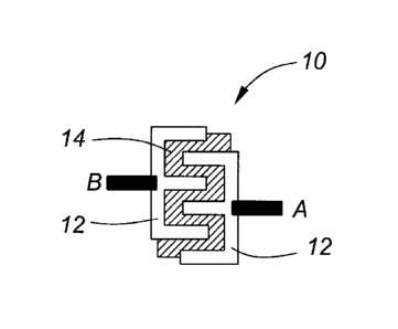
Referring now to Figure 1 a variable capacitor or varactor 10 is shown formed
by printing a
single layer of interdigitated lines using a conductive ink 12, with the gaps
between these
lines of conductive ink filled with a ferroelectric printed ink 14. The two
ends of the capacitor
10, labeled A and B in Figure 1 are resistive bias lines printed with
resistive ink. It should be
understood that after the printed ink dries or cures, it becomes dried or
cured ink, referred to
hereafter as material or printed material. By applying a DC voltage to the
bias lines A and B,
the permittivity of the ferroelectric material 14 will change, which causes a
change in the
capacitance value of the varactor. A varying voltage over a range of voltages
will result in a
varying capacitance. In one embodiment, the varactor and biasing circuitry are
integrated
using a single monolithic printing process. In a less preferred embodiment the
resistivity of
the ink of the bias lines could range from about 4 to 25 milliohms per square
per mil, however
in more practicable useful embodiments having a large number of interconnected
varactors, in
order to have less loss, a higher resistance is required. For example in
arrays of varactors
resistive bias lines would be about 100 ohms or more per square millimetre
preferably for
large arrays, several hundred ohms per square per mil or higher.
In another embodiment, a metal-insulator-metal (MIM) capacitor 20 is shown in
Figure 2. In
this embodiment, multi-layer printing is required, where two metal plates 22a
and 22b of the
varactor are printed on different layers supported by the substrate 24,
separated by printed
8
CA 3002992 2018-04-26
Doc. No. 102-75 CA
ferroelectric material 26, which acts as an insulator with controllable
dielectric properties. The
interdigital design of Figure 1 has the advantage of being printed as a single
layer, but will
require a higher bias voltage in order to change the permittivity of the
ferroelectric material
14, thereby changing the capacitance value of the varactor. The MIM structure
20 requires a
multi-layer printing process, but will need less DC bias voltage to change the
permittivity of
the ferroelectric material 26. This structure lends itself to use in large
arrays of MIM
varactors.
Turning now to Figure 3(a), an embodiment of an electronically reconfigurable
EES 31
designed to be fabricated using printed electronics technology is shown. It
uses the basic
interdigital varactor cell 10 of Figure I, where resistive material 33a, 33b
is printed forming
the bias lines G and H to isolate radio frequency (RF) and direct current (DC)
signals and
where ferroelectric material 34 is used to enable electronic control. The unit
cell 35 of the
EES, as identified in Figure 3(a), consists of a square loop resonator 36 with
an interdigital
varactor 30 integrated in each side of the loop, wherein the varactors 30 are
interconnected by
printed conductive material 32 forming the loop. Each loop, has printed a
plurality of resistive
bias input lines. Dielectric material 37 is used as an insulator to prevent
certain paths from
electrically contacting one another. Applying a DC voltage bias to the
structure causes the
permittivity of the ferroelectric material 34 to change, which changes the
capacitance of the
varactor 30 and which, in turn, changes the resonant frequency of the square
loop resonator.
This allows for the dynamic tuning of the resonant frequency at which the EES
31 either
blocks or passes through incoming radio-wave signals. The actual EES 31 may
include
hundreds or thousands of these voltage controllable unit cells arranged in a
regular lattice
configuration; only a few unit cells are shown in Figure 3(a) along with a
close-up view of
two neighboring cells. One of the distinguishing features of this embodiment
is the use of DC
bias lines G and H, integrated with the EES 31 in the same monolithic process.
Figure 3(c) shows a second embodiment where MIM varactors 20 as described in
Figure 2 are
used instead of interdigital varactors 30 of Figure 3 (a). The principle of
operation is the same
as the embodiment of Figure 3(a), but a smaller value of DC bias voltage would
be required to
obtain the same varactor tuning range. The varactors are coupled with
conductive printed
9
CA 3002992 2018-04-26
Doc. No. 102-75 CA
material 46 and resistive printed paths are shown as 48b. Dielectric printed
material 47 is
shown providing required insulation.
A salient feature of the suggested cell element of this invention is a self-
resonating structure.
Specifically, the proposed cell element described using interdigitated
varactors 10 or MIM
varactors 20 is a square loop, which is preferably loaded on each of its four
sides by
interdigital capacitors (IDC). This contrasts the design in where the
capacitive loading is done
between cell elements, not within the same cell element. In this invention,
the capacitive
loading within the cell element tends to shrink the size of the cell element,
which improves
the angular stability of the resulting FSS structure; advantageously its
behavior is less
sensitive to the angle of incidence of the incoming radio signals.
For embodiments shown in Figures 3(a), 3(b) and 3(c), no external bias
circuitry is required to
change the capacitance of the varactor elements, as it is seamlessly
integrated within the EES
structure. A second distinguishing feature is that these DC bias lines are
fabricated using
resistive inks, in contrast to the conventional approach using conductive DC
bias lines, and
thus nearly appear transparent to the radio-frequency (RF) behaviour of the
EES, and have
negligible or no negative impact on performance. Resistance on the order of at
least a few
hundred ohms would be typical in order for the bias lines to appear RF
transparent. The use of
these resistive bias lines is also closely linked to the integration of the
varactor elements in the
EES, which only require a DC voltage in order to control their capacitance.
By using a varactor element as described heretofore, advantageously, there is
no continuous
path for DC current to flow; the flow of significant DC current along highly
resistive bias
lines would result in substantial unwanted losses from voltage drops. Other
devices such as
certain diodes or transistors, for example that rely on DC bias currents could
not be biased by
resistive bias lines without incurring significant losses.
The embodiments of the invention described make use of a combination of
ferroelectric inks
with at least one of conductive, dielectric, and resistive inks printed in a
multi-layer process,
along with patterning designs that allow for the monolithic fabrication of the
required active
CA 3002992 2018-04-26
Doc. No. 102-75 CA
devices and biasing circuitry for electronically controlling reconfigurable
EESs. Methods for
integrating such circuitry without disturbing the RF performance of the EES
have previously
posed a significant design challenge. However, in this invention, signal lines
of the bias
circuitry are formed by resistive segments, which are seamlessly routed
throughout the EES
structure formed by printing the conductive, dielectric and ferroelectric inks
so as to minimize
any impact on the RE performance of the EES. The resultant invention allows
scalability of
the EES in both size and frequency.
As mentioned above, the conductive, dielectric, resistive and ferroelectric
inks are
commercially available. Conductive inks, in particular are often composed of
flakes of metal
nanoparticles or silver or copper-based molecular inks such as those, for
example, described
in PCT/CA2015/050568.
The flow process for fabrication is depicted in Figure 4 where the numbering
scheme
corresponds to the sequence of the application of inks. For this particular
embodiment, the
substrate onto which the inks are printed is a flexible plastic (PET) of 5 mil
thickness. Printing
would also work well on thinner or thicker flexible plastic materials such as
Kapton or Mylar,
and the process could be adjusted to print on other materials such as papers,
glass, or fabrics
(textiles). The process flow is designed for screen-printing, but could also
be adapted to other
printing methods such as inkjet printing or any other printed electronics
technology that is
capable of multi-layer printing at the required resolution. The process could
also be applied to
rigid substrates such as rigid plastics, glass, or directly onto construction
material like drywall
or concrete. The separation between two adjacent unit cell elements is 4.0 mm
in this specific
case for operation at 28.00Hz. The minimum line width and minimum gap between
conductors was set to 75 IM1 to meet fabrication tolerances of print
technology.
By using a combination of different printed electronic inks, for example,
conductive, resistive,
dielectric, and ferroelectric inks deposited on different layers, the
electronically
reconfigurable EES can be manufactured in a single process and be fully
printable without the
requirement for hybrid integration of separate, discrete devices, allowing the
design to be
scalable to large surface areas. Due to the fine feature sizes that can be
printed using current
11
CA 3002992 2018-04-26
Doc. No. 102-75 CA
printed electronics technology, this design is also scalable to millimeter-
wave frequencies. As
the minimum feature size attainable by printed electronics continues to
shrink, the maximum
frequency to which the invention can be designed will continue to increase,
eventually
possibly up to the Terahertz range. In short, the ability of printed
electronics technology to
deposit different types of inks in multiple layers onto large area flexible
surfaces, combined
with EES designs to exploit this capability and seamlessly incorporate biasing
circuitry to
develop electronically reconfigurable EES, offers significant advantages.
Combining printed electronics having printed biasing circuitry and novel EES
designs,
enables the production of low-cost, flexible electronically reconfigurable EES
that are
scalable in both size and frequency, which is a capability unavailable to any
other technology
or design. Furthermore, as new advancements are made in printed electronics
technologies
based on developments or improvements in semiconductor, carbon-nanotube, or
other inks,
this will enable new or enhance the current capabilities in electronically
controlled
reconfigurable EESs and extend the frequency limit to which these EESs can be
scaled,
possibly up to the terahertz range. Also, it is envisioned that the capacitive
components could
eventually be replaced by printed transistor switches using semi-or conductive
ink.
Figure 5 shows another embodiment of a reconfigurable EES unit cell 50, which
is of a cross
shape, compared to the square loop shape shown heretofore.
Again, the varactor elements 52, consisting of interdigital capacitors, form
part of the element
itself, and would be filled with ferroelectric material and biased with
resistive lines 54 in
order to shift the frequency of operation of the EES. In such an embodiment,
this element can
form part of an antenna array, and individually controlling the DC bias to
each of these
radiators would enable the electronic reconfiguration of the antenna radiation
pattern. In
another embodiment, these ferroelectric-filled capacitors could form phase-
shifting elements
that are integrated within the beam-forming network of an antenna array and
would be
individually controlled to electronically reconfigure the radiation pattern.
The behaviour of electronically reconfigurable EESs has been simulated using
commercially
12
CA 3002992 2018-04-26
Doc. No. 102-75 CA
available electromagnetic simulation software: High-Frequency Simulation
Software (HFSS).
Figure 6 shows the simulated transmission behaviour of the electronically
reconfigurable EES
design of Figure 3(a), where the ferroelectric material is assumed to have a
tunability of 10%.
Without DC voltage bias, the EES is designed to block frequencies centred
around 25 GHz
.. shown by the solid curve in Figure 6. When the maximum value of DC bias is
applied to
cause a 10% shift in the permittivity of the ferroelectric material from a
value of 36 to 40, the
blocking centre frequency shifts from 25 GHz to approximately 22.6 GHz
indicated by the
dashed curve. If the application of interest is at 25 GI-1z, then the
application and removal of
the DC bias will cause the surface to either allow or block these RF signals
to pass through,
thus the EES can be switched on and off using DC voltage bias control.
Some embodiments of this invention apply to the field of EESs, where an
intended application
is deployment over wide surfaces, either indoor or outdoor, in such a way as
to enhance the
radio-propagation environment, by either blocking, re-directing, or letting
pass specific radio
frequency (RF) signals for mitigating interfering signals or for enhancing
coverage in wireless
communication systems. Based on fabrication using current printed electronics
technology,
the invention is scalable to current and planned cellular and WiFi bands up to
the millimeter-
wave bands being considered for use by future 5G wireless communications
applications. As
printed electronics technology improves, allowing for the printing of smaller
and smaller
feature sizes, the invention would be scalable to higher frequencies, possibly
up to the
Terahertz range.
Turning now of Figure 7(a), an ESS having organic thin-film transistors
(OTFTs) at have
been printed using conductive, dielectric, semiconductor, and resistive inks.
Conductive ink
.. 72 forms the Gate (G), Source (S) and Drain (D) terminals of the
transistor. A layer of
dielectric ink 74 and a layer of semiconductor ink 76 is printed between the G
terminal and
the S and D terminals. Four unit cells are shown in Figure 7(a). A circuit
representation of an
OTFT is shown in Figure 7(b).
Figure 8 illustrates an exemplary embodiment of a portion of an engineered
electromagnetic
surface (EES) with embedded OTFTs 83. The EES 80 is shown having cross-shaped
elements
13
CA 3002992 2018-04-26
Doc. No. 102-75 CA
82 with the OTFTs 83 integrated into the arms 84 of the cross shaped elements
82. Resistive
bias lines (not shown) are connected to the gate (G) terminals of the OTFT 83,
while the cross
segments, formed from a conductive ink 82, are connected to either the source
(S) or drain
(D) terminals of the OFTFs 83. When the OFTFs 83 are biased in their OFF
state, they act as
.. open circuits, and the arms of the cross have an effective length of L 1,
resulting in a resonant
frequency of Fl. When the OFTFs 83 are biased in their ON state, they form a
short circuit,
connecting the segments of the cross arms to form an effective length of L2,
resulting in a
resonant frequency of F2. Thus, biasing the OFTFs 83 OFF or ON will result in
the EES 80
from switching operation from frequency F! to frequency F2. Frequencies Fl and
F2 can be
widely separated, since they are controlled solely by the lengths of the cross
arm segments
(L1 and L2). This differs from the varactor-tuned EES designs, where applying
the bias will
only result in tuning the frequency of operation by a small percentage around
the original
resonant frequency.
It should be understood that the terms "printed thereon" or "printed on the
substrate" when
referring to ink printed on the substrate can mean directly on and contacting
the substrate or
over a layer carried by the substrate such as a layer that has been printed on
the substrate,
wherein all of these layers are supported by the substrate.
14
CA 3002992 2018-04-26