Note: Descriptions are shown in the official language in which they were submitted.
CA 03003070 2018-04-24
=
- 1 -
A METHOD FOR MANUFACTURING A MEMBRANE ASSEMBLY
FIELD
[0002] The present invention relates to a method for manufacturing a
membrane
assembly, and to a membrane assembly.
BACKGROUND
[0003] A lithographic apparatus is a machine that applies a desired
pattern onto a
substrate, usually onto a target portion of the substrate. A lithographic
apparatus can be used,
for example, in the manufacture of integrated circuits (ICs). In that
instance, a patterning
device, which is alternatively referred to as a mask or a reticle, may be used
to generate a
circuit pattern to be formed on an individual layer of the IC. This pattern
can be transferred
onto a target portion (e.g., comprising part of, one, or several dies) on a
substrate (e.g., a
silicon wafer). Transfer of the pattern is typically via imaging onto a layer
of radiation-
sensitive material (resist) provided on the substrate. In general, a single
substrate will contain
a network of adjacent target portions that are successively patterned.
[0004] Lithography is widely recognized as one of the key steps in the
manufacture
of ICs and other devices and/or structures. However, as the dimensions of
features made
using lithography become smaller, lithography is becoming a more critical
factor for enabling
miniature IC or other devices and/or structures to be manufactured.
[0005] A theoretical estimate of the limits of pattern printing can be
given by the
Rayleigh criterion for resolution as shown in equation (1):
CD = k, *A, (1)
NA
where X is the wavelength of the radiation used, NA is the numerical aperture
of the
projection system used to print the pattern, kl is a process-dependent
adjustment factor, also
called the Rayleigh constant, and CD is the feature size (or critical
dimension) of the printed
CA 03003070 2018-04-24
WO 2017/076686
PCT/EP2016/075605
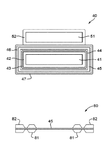
- 2 -
feature. It follows from equation (1) that reduction of the minimum printable
size of features
can be obtained in three ways: by shortening the exposure wavelength k, by
increasing the
numerical aperture NA or by decreasing the value of kl.
[0006] In order to shorten the exposure wavelength and, thus, reduce
the minimum
printable size, it has been proposed to use an extreme ultraviolet (EUV)
radiation source.
EUV radiation is electromagnetic radiation having a wavelength within the
range of
10-20 nm, for example within the range of 13-14 nm. It has further been
proposed that EUV
radiation with a wavelength of less than 10 nm could be used, for example
within the range of
5-10 nm such as 6.7 nm or 6.8 nm. Such radiation is termed extreme ultraviolet
radiation or
soft x-ray radiation. Possible sources include, for example, laser-produced
plasma sources,
discharge plasma sources, or sources based on synchrotron radiation provided
by an electron
storage ring.
[0007] A lithographic apparatus includes a patterning device (e.g., a
mask or a
reticle). Radiation is provided through or reflected off the patterning device
to form an image
on a substrate. A membrane assembly may be provided to protect the patterning
device from
airborne particles and other forms of contamination. The membrane assembly for
protecting
the patterning device may be called a pellicle. Contamination on the surface
of the patterning
device can cause manufacturing defects on the substrate. The membrane assembly
may
comprise a border and a membrane stretched across the border. It is difficult
to manufacture
the membrane assembly without the membrane assembly being deformed in the
process, for
example because of the thinness of the membrane.
[0008] It is also difficult to manufacture the membrane assembly
without the
membrane assembly being damaged in the process. For example, the membrane may
be
undesirably oxidized during the process of manufacturing the membrane
assembly.
[0009] It is desirable to reduce the possibility of a membrane assembly
such as a
pellicle being deformed or damaged during its manufacture. It is also
desirable to reduce the
time it takes to manufacture a membrane assembly.
SUMMARY OF THE INVENTION
[0010] According to an aspect of the invention, there is provided a method
for
manufacturing a membrane assembly for EUV lithography, the method comprising:
providing a stack comprising a membrane layer between a supporting substrate
and an
attachment substrate, wherein the supporting substrate comprises an inner
region and a first
CA 03003070 2018-04-24
WO 2017/076686
PCT/EP2016/075605
- 3 -
border region; processing the stack, including selectively removing the inner
region of the
supporting substrate, to form a membrane assembly comprising: a membrane
formed from at
least the membrane layer; and a support holding the membrane, the support
foimed at least
partially from the first border region of the supporting substrate.
[0011] According to an aspect of the invention, there is provided a
membrane
assembly for EUV lithography, the membrane assembly comprising: a membrane;
and a
support holding the membrane, the support foimed from a first border region of
a supporting
substrate and a second border region of an attachment substrate, wherein the
membrane is
between the first border region of the supporting substrate and the second
border region of
the attachment substrate; wherein the support is formed by selectively
removing an inner
region of the supporting substrate and a cover region of the attachment
substrate such that the
first border region of the supporting substrate and the second border region
of the attachment
substrate remain.
[0012] According to an aspect of the invention, there is provided a
method for
manufacturing a membrane assembly for a lithographic apparatus, the method
comprising
providing a supporting substrate having an average thickness of at least 600
gm, preferably at
least 700 gm, with a membrane layer; wafer bonding an attachment substrate
having an
average thickness of less than 500 gm to the supporting substrate provided
with the
membrane layer to form a stack, wherein the membrane layer is encapsulated
between the
supporting substrate and the attachment substrate; and subsequently thinning
the supporting
substrate bonded to the attachment substrate to an average thickness of the
supporting
substrate to be less than 500 gm. Preferably the thickness of the supporting
substrate and the
thickness of the attachment substrate are substantially equal, in order to
form a substantially
symmetrical stack.
BRIEF DESCRIPTION OF THE DRAWINGS
[0013] Embodiments of the invention will now be described, by way of
example only,
with reference to the accompanying schematic drawings in which corresponding
reference
symbols indicate corresponding parts, and in which:
[0014] Figure 1 depicts a lithographic apparatus according to an embodiment
of the
invention;
[0015] Figure 2 is a more detailed view of the lithographic apparatus;
CA 03003070 2018-04-24
WO 2017/076686
PCT/EP2016/075605
- 4 -
[0016] Figures 3 to 19 schematically depict stages of a method for
manufacturing a
pellicle according to an embodiment of the invention;
[0017] Figures 20 to 29 schematically depict stages of an alternative
method for
manufacturing a pellicle according to an embodiment of the invention;
[0018] Figures 30 to 37 schematically depict stages of an alternative
method for
manufacturing a pellicle according to an embodiment of the invention;
[0019] Figures 38 to 45 schematically depict stages of an alternative
method for
manufacturing a pellicle according to an embodiment of the invention;
[0020] Figures 46 to 49 schematically depict stages of an alternative
method for
manufacturing a pellicle according to an embodiment of the invention; and
[0021] Figures 50 to 52 schematically depict stages of an alternative
method for
manufacturing a pellicle according to an embodiment of the invention;
[0022] The features and advantages of the present invention will
become more
apparent from the detailed description set forth below when taken in
conjunction with the
drawings, in which like reference characters identify corresponding elements
throughout. In
the drawings, like reference numbers generally indicate identical,
functionally similar, and/or
structurally similar elements.
DETAILED DESCRIPTION
[0023] Figure 1 schematically depicts a lithographic apparatus 100
including a source
collector module SO according to one embodiment of the invention. The
apparatus 100
comprises:
- an illumination system (or illuminator) IL configured to condition a
radiation beam B
(e.g., BUY radiation).
- a support structure (e.g., a mask table) MT constructed to support a
patterning device
(e.g., a mask or a reticle) MA and connected to a first positioner PM
configured to accurately
position the patterning device;
- a substrate table (e.g., a wafer table) WI' constructed to hold a
substrate (e.g., a
resist-coated wafer) W and connected to a second positioner PW configured to
accurately
position the substrate; and
- a projection system (e.g., a reflective projection system) PS configured
to project a
pattern imparted to the radiation beam B by patterning device MA onto a target
portion C
(e.g., comprising one or more dies) of the substrate W.
CA 03003070 2018-04-24
WO 2017/076686
PCT/EP2016/075605
- 5 -
[0024] The illumination system IL may include various types of optical
components,
such as refractive, reflective, magnetic, electromagnetic, electrostatic or
other types of optical
components, or any combination thereof, for directing, shaping, or controlling
radiation.
[0025] The support structure MT holds the patterning device MA in a
manner that
depends on the orientation of the patterning device, the design of the
lithographic apparatus,
and other conditions, such as for example whether or not the patterning device
is held in a
vacuum environment. The support structure MT can use mechanical, vacuum,
electrostatic or
other clamping techniques to hold the patterning device MA. The support
structure MT may
be a frame or a table, for example, which may be fixed or movable as required.
The support
structure MT may ensure that the patterning device MA is at a desired
position, for example
with respect to the projection system PS.
[0026] The term "patterning device" should be broadly interpreted as
referring to any
device that can be used to impart a radiation beam B with a pattern in its
cross-section such as
to create a pattern in a target portion C of the substrate W. The pattern
imparted to the
radiation beam B may correspond to a particular functional layer in a device
being created in
the target portion C, such as an integrated circuit.
[0027] The patterning device MA may be transmissive or reflective.
Examples of
patterning devices include masks, programmable mirror arrays, and programmable
liquid-
crystal display (LCD) panels. Masks are well known in lithography, and include
mask types
such as binary, alternating phase-shift, and attenuated phase-shift, as well
as various hybrid
mask types. An example of a programmable mirror array employs a matrix
arrangement of
small mirrors, each of which can be individually tilted so as to reflect an
incoming radiation
beam in different directions. The tilted mirrors impart a pattern in a
radiation beam, which is
reflected by the mirror matrix.
[0028] The projection system PS, like the illumination system IL, may
include
various types of optical components, such as refractive, reflective, magnetic,
electromagnetic,
electrostatic or other types of optical components, or any combination
thereof, as appropriate
for the exposure radiation being used, or for other factors such as the use of
a vacuum. It may
be desired to use a vacuum for EUV radiation since other gases may absorb too
much
radiation. A vacuum environment may therefore be provided to the whole beam
path with the
aid of a vacuum wall and vacuum pumps.
[0029] As here depicted, the lithographic apparatus 100 is of a
reflective type (e.g.,
employing a reflective mask).
CA 03003070 2018-04-24
WO 2017/076686
PCT/EP2016/075605
- 6 -
[0030] The lithographic apparatus 100 may be of a type having two
(dual stage) or
more substrate tables WT (and/or two or more support structures MT). In such a
"multiple
stage" lithographic apparatus the additional substrate tables WT (and/or the
additional
support structures MT) may be used in parallel, or preparatory steps may be
carried out on
one or more substrate tables WT (and/or one or more support structures MT)
while one or
more other substrate tables WT (and/or one or more other support structures
MT) are being
used for exposure.
[0031] Referring to Figure 1, the illumination system IL receives an
extreme
ultraviolet radiation beam from the source collector module SO. Methods to
produce EUV
light include, but are not necessarily limited to, converting a material into
a plasma state that
has at least one element, e.g., xenon, lithium or tin, with one or more
emission lines in the
EUV range. In one such method, often termed laser produced plasma ("LPP") the
required
plasma can be produced by irradiating a fuel, such as a droplet, stream or
cluster of material
having the required line-emitting element, with a laser beam. The source
collector module SO
may be part of an EUV radiation system including a laser, not shown in Figure
1, for
providing the laser beam exciting the fuel. The resulting plasma emits output
radiation, e.g.,
EUV radiation, which is collected using a radiation collector, disposed in the
source collector
module. The laser and the source collector module SO may be separate entities,
for example
when a CO2 laser is used to provide the laser beam for fuel excitation.
[0032] In such cases, the laser is not considered to form part of the
lithographic
apparatus 100 and the radiation beam B is passed from the laser to the source
collector
module SO with the aid of a beam delivery system comprising, for example,
suitable
directing mirrors and/or a beam expander. In other cases the source may be an
integral part of
the source collector module SO, for example when the source is a discharge
produced plasma
EUV generator, often termed as a DPP source.
[0033] The illumination system IL may comprise an adjuster for
adjusting the angular
intensity distribution of the radiation beam. Generally, at least the outer
and/or inner radial
extent (commonly referred to as a-outer and a-inner, respectively) of the
intensity
distribution in a pupil plane of the illumination system IL can be adjusted.
In addition, the
illumination system IL may comprise various other components, such as facetted
field and
pupil mirror devices. The illumination system IL may be used to condition the
radiation beam
B, to have a desired uniformity and intensity distribution in its cross-
section.
CA 03003070 2018-04-24
WO 2017/076686
PCT/EP2016/075605
- 7 -
[0034] The radiation beam B is incident on the patterning device
(e.g., mask) MA,
which is held on the support structure (e.g., mask table) MT, and is patterned
by the
patterning device MA. After being reflected from the patterning device (e.g.,
mask) MA, the
radiation beam B passes through the projection system PS, which focuses the
radiation beam
B onto a target portion C of the substrate W. With the aid of the second
positioner PW and
position sensor PS2 (e.g., an interferometric device, linear encoder or
capacitive sensor), the
substrate table WT can be moved accurately, e.g., so as to position different
target portions C
in the path of the radiation beam B. Similarly, the first positioner PM and
another position
sensor PS1 can be used to accurately position the patterning device (e.g.,
mask) MA with
respect to the path of the radiation beam B. The patterning device (e.g.,
mask) MA and the
substrate W may be aligned using mask alignment marks Ml, M2 and substrate
alignment
marks P1, P2.
[0035] A controller 500 controls the overall operations of the
lithographic apparatus
100 and in particular performs an operation process described further below.
Controller 500
can be embodied as a suitably-programmed general purpose computer comprising a
central
processing unit, volatile and non-volatile storage means, one or more input
and output
devices such as a keyboard and screen, one or more network connections and one
or more
interfaces to the various parts of the lithographic apparatus 100. It will be
appreciated that a
one-to-one relationship between controlling computer and lithographic
apparatus 100 is not
necessary. In an embodiment of the invention one computer can control multiple
lithographic
apparatuses 100. In an embodiment of the invention, multiple networked
computers can be
used to control one lithographic apparatus 100. The controller 500 may also be
configured to
control one or more associated process devices and substrate handling devices
in a lithocell or
cluster of which the lithographic apparatus 100 forms a part. The controller
500 can also be
configured to be subordinate to a supervisory control system of a lithocell or
cluster and/or an
overall control system of a fab.
[0036] Figure 2 shows the lithographic apparatus 100 in more detail,
including the
source collector module SO, the illumination system II, and the projection
system PS. An
EUV radiation emitting plasma 210 may be formed by a plasma source. EUV
radiation may
be produced by a gas or vapor, for example Xe gas, Li vapor or Sn vapor in
which the
radiation emitting plasma 210 is created to emit radiation in the EUV range of
the
electromagnetic spectrum. In an embodiment, a plasma of excited tin (Sn) is
provided to
produce EUV radiation.
CA 03003070 2018-04-24
WO 2017/076686
PCT/EP2016/075605
- 8 -
[0037] The radiation emitted by the radiation emitting plasma 210 is
passed from a
source chamber 211 into a collector chamber 212.
[0038] The collector chamber 212 may include a radiation collector CO.
Radiation
that traverses the radiation collector CO can be focused in a virtual source
point IF. The
virtual source point IF is commonly referred to as the intermediate focus, and
the source
collector module SO is arranged such that the virtual source point IF is
located at or near an
opening 221 in the enclosing structure 220. The virtual source point IF is an
image of the
radiation emitting plasma 210.
[0039] Subsequently the radiation traverses the illumination system
IL, which may
include a facetted field mirror device 22 and a facetted pupil mirror device
24 arranged to
provide a desired angular distribution of the unpatterned beam 21, at the
patterning device
MA, as well as a desired uniformity of radiation intensity at the patterning
device MA. Upon
reflection of the unpatterned beam 21 at the patterning device MA, held by the
support
structure MT, a patterned beam 26 is formed and the patterned beam 26 is
imaged by the
projection system PS via reflective elements 28, 30 onto a substrate W held by
the substrate
table WT.
[0040] More elements than shown may generally be present in the
illumination
system IL and the projection system PS. Further, there may be more mirrors
present than
those shown in the Figures, for example there may be 1- 6 additional
reflective elements
present in the projection system PS than shown in Figure 2.
[0041] Alternatively, the source collector module SO may be part of an
LPP radiation
system.
[0042] As depicted in Figure 1, in an embodiment the lithographic
apparatus 100
comprises an illumination system IL and a projection system PS. The
illumination system IL
is configured to emit a radiation beam B. The projection system PS is
separated from the
substrate table WT by an intervening space. The projection system PS is
configured to project
a pattern imparted to the radiation beam B onto the substrate W. The pattern
is for EU V
radiation of the radiation beam B.
[0043] The space intervening between the projection system PS and the
substrate
table WT can be at least partially evacuated. The intervening space may be
delimited at the
location of the projection system PS by a solid surface from which the
employed radiation is
directed toward the substrate table WT.
CA 03003070 2018-04-24
WO 2017/076686
PCT/EP2016/075605
- 9 -
[0044] In an embodiment the lithographic apparatus 100 comprises a
dynamic gas
lock. The dynamic gas lock comprises a membrane assembly 80. In an embodiment
the
dynamic gas lock comprises a hollow part covered by a membrane assembly 80
located in the
intervening space. The hollow part is situated around the path of the
radiation. In an
embodiment the lithographic apparatus 100 comprises a gas blower configured to
flush the
inside of the hollow part with a flow of gas. The radiation travels through
the membrane
assembly before impinging on the substrate W.
[0045] In an embodiment the lithographic apparatus 100 comprises a
membrane
assembly 80. As explained above, in an embodiment the membrane assembly 80 is
for a
dynamic gas lock. In this case the membrane assembly 80 functions as a filter
for filtering
DUV radiation. Additionally or alternatively, in an embodiment the membrane
assembly 80
is pellicle for the patterning device MA for EUV lithography. The membrane
assembly 80 of
the present invention can be used for a dynamic gas lock or for a pellicle or
for another
purpose such as a spectral purity filter. In an embodiment the membrane
assembly 80
comprises a membrane, which may also be called a membrane stack. The membrane
of the
membrane assembly 80 comprises a membrane layer 45 and optionally capping
films
(described later). When the membrane of the membrane assembly 80 comprises the
membrane layer 45 and at least one capping film (layer) then it may be called
a membrane
stack. The membrane layer 45 may also be a multilayer membrane layer 45 formed
by a
plurality of alternating layers of two or more different materials, in which
case a capping film
will have a different material than the alternating layers in the multilayer
membrane layer 45.
In an embodiment the membrane of the membrane assembly 80 is configured to
transmit at
least 80% of incident EUV radiation.
[0046] In an embodiment the pellicle is configured to seal off the
patterning device
MA to protect the patterning device MA from airborne particles and other forms
of
contamination. Contamination on the surface of the patterning device MA can
cause
manufacturing defects on the substrate W. For example, in an embodiment the
pellicle is
configured to reduce the likelihood that particles might migrate into a
stepping field of the
patterning device MA in the lithographic apparatus 100.
[0047] If the patterning device MA is left unprotected, the contamination
can require
the patterning device MA to be cleaned or discarded. Cleaning the patterning
device MA
interrupts valuable manufacturing time and discarding the patterning device MA
is costly.
Replacing the patterning device MA also interrupts valuable manufacturing
time.
CA 03003070 2018-04-24
WO 2017/076686
PCT/EP2016/075605
- 10-
[0048] Figures 3 and 4 schematically depict stages of a method for
manufacturing the
membrane assembly 80 according to an embodiment of the invention. In an
embodiment the
method for manufacturing the membrane assembly 80 comprises providing a
supporting
substrate 41 for a stack 40.
[0049] In an embodiment the supporting substrate 41 is a wafer formed from
silicon.
The supporting substrate 41 has a shape such as a square, a circle or a
rectangle, for example.
The shape of the supporting substrate 41 is not particularly limited. The size
of the supporting
substrate 41 is not particularly limited. For example, in an embodiment the
supporting
substrate 41 has a diameter in the range of from about 100 mm to about 500 mm,
for example
about 200 mm. The thickness of the supporting substrate 41 is not particularly
limited. For
example, in an embodiment the supporting substrate 41 has a thickness of at
least 300 gm,
optionally at least 400 gm. In an embodiment the supporting substrate 41 has a
thickness of at
most 1,000 gm, optionally at most 800 gm. In an embodiment the supporting
substrate 41 has
a thickness of at most 600 gm, optionally at most 400 gm. In an embodiment the
supporting
.. substrate 41 has a thickness of about 400 gm. By providing a thinner
supporting substrate 41,
the amount of the supporting substrate 41 that needs to be selectively removed
is reduced.
Accordingly, by starting with a thinner supporting substrate 41, an embodiment
of the
invention is expected to reduce the possibility of the membrane being damaged
or
contaminated during the step of selectively removing parts of the supporting
substrate 41.
Additionally, by starting with a supporting substrate 41, an embodiment of the
invention is
expected to make the manufacturing process more efficient.
[0050] Silicon can crystallise in a diamond cubic crystal structure.
In an embodiment
the supporting substrate 41 comprises a cubic crystal of silicon. In an
embodiment the
supporting substrate 41 has a <100> crystallographic direction.
[0051] As depicted in Figure 4, in an embodiment the supporting substrate
41
comprises a sacrificial layer. The sacrificial layer may be for example an
oxidized layer 42.
The oxidized layer 42 is part of the supporting substrate 41. The rest of the
supporting
substrate 41 forms a non-oxidized layer of the supporting substrate 41. The
oxidized layer 42
foims an etch barrier when at least a part of the non-oxidized layer of the
supporting substrate
41 is removed, for example is etched away. As depicted in Figure 16, for
example, the
supporting substrate 41 is etched from the bottom side. The oxidized layer 42
is resistant to
the wet etchant. In an embodiment the oxidized layer 42 can be replaced by an
alternative
sacrificial layer that is not an oxide layer.
CA 03003070 2018-04-24
WO 2017/076686
PCT/EP2016/075605
- 11 -
[0052] In an embodiment the oxidized layer 42 has a thickness greater
than 100 nm,
optionally greater than 200 nm, and optionally greater than 300 nm. For
example, in an
embodiment the oxidized layer 42 has a thickness of about 350 nm or about 400
nm. An
embodiment of the invention is expected to achieve an improved robustness in a
step of
etching at least part of the supporting substrate 41.
[0053] In an embodiment the oxidized layer 42 is formed as a thin
layer of oxide on
outer surfaces of the supporting substrate 41. In an embodiment the oxidized
layer 42 is
formed by a thermal oxidation process, for example as a thermal wet oxide. In
an
embodiment the oxidized layer 42 and the etchant used for etching at least
part of the
supporting substrate 41 are configured such that there is a good/high enough
selectivity of the
sacrificial layer (e.g. oxidized layer 42) with respect to the underlying
layer (e.g. supporting
substrate 41). For example, in an embodiment the etch rate of the oxidized
layer 42 in the
etchant is less than about 5 nm/minute, for example about 3 nm/minute. In an
embodiment
the oxidized layer 42 comprises amorphous silicon dioxide.
[0054] The oxidized layer 42 is optional. In an embodiment the oxidized
layer 42 is
not provided. If the oxidized layer 42 is not provided, an alternative etch
stop may be
provided, or the step of etching the supporting substrate 41 may be controlled
such so as to
reduce the possibility of part of the membrane of the membrane assembly 80
being
undesirably etched away.
[0055] As depicted in Figure 5, in an embodiment the stack 40 comprises a
lower
capping film 44. The lower capping film 44 is disposed between the supporting
substrate 41
and the membrane layer 45. As depicted in Figure 3, in an embodiment the stack
40
comprises an optional lower sacrificial layer 43. The lower sacrificial layer
43 is disposed
between the supporting substrate 41 and the membrane layer 45.
[0056] When the stack 40 comprises the lower sacrificial layer 43, the
lower capping
film 44 is disposed between the lower sacrificial layer 43 and the membrane
layer 45. In an
embodiment the lower capping film 44 forms part of the membrane of the
membrane
assembly 80 produced by the method according to an embodiment of the
invention.
[0057] The thickness of the lower sacrificial layer 43 is not
particularly limited. In an
embodiment the thickness of the lower sacrificial layer 43 is at least about 5
nm, and
optionally at least about 10 nm. In an embodiment the thickness of the lower
sacrificial layer
43 is at most about 100 nm. and optionally at most about 50 nm. In an
embodiment the
CA 03003070 2018-04-24
WO 2017/076686
PCT/EP2016/075605
- 1', -
thickness of the lower sacrificial layer 43 is at most about 1000 nm and at
least about 5 nm,
but preferably at most 100 and at least 20 nm.
[0058] In an embodiment the lower sacrificial layer 43 is formed from
a material such
as amorphous silicon. However, this is not necessarily the case.
[0059] The method of depositing the lower sacrificial layer 43 onto the
stack 40 is not
particularly limited. In an embodiment the lower sacrificial layer 43 is
applied to the stack 40
by chemical vapor deposition, for example low pressure chemical vapor
deposition (LPCVD)
or plasma-enhanced chemical vapor deposition (PECVD). LPCVD produces layers of
relatively high quality while PECVD can desirably be effected at lower
temperatures. For
example, in an embodiment the lower sacrificial layer 43 is applied to the
stack 40 by
LPCVD at a temperature in a range from 300 to 700 C. However, this is not
necessarily the
case. For example, in an alternative embodiment the lower sacrificial layer 43
is applied to
the stack 40 by PECVD, a sputtering method or by a thin film deposition
method, for
example.
[0060] In an embodiment, each of the lower capping film 44 and the upper
capping
film 46 has a thickness of less than 10 nm, preferably less than 4 nm. In an
embodiment the
combined thickness of the lower capping film 44, the membrane layer 45 and the
upper
capping film 46 is approximately 50 nm. In an embodiment the material for the
upper
capping film 46 is the same as the material for the lower capping film 44.
[0061] For example, in an embodiment the membrane layer 45 is formed from
polycrystalline or nanocrystalline silicon. Polycrystalline or nanocrystalline
silicon has a
brittle nature. Hence, a membrane assembly 80 comprising a membrane that
comprises a
membrane layer 45 formed from polycrystalline or nanocrystalline silicon can
shatter into
many particles when the membrane assembly 80 breaks. An embodiment of the
invention is
expected to achieve an improvement in the mechanical properties of the
membrane assembly
80.
[0062] Polycrystalline silicon and nanocrystalline silicon each have
high transmission
for EUV radiation. Polycrystalline silicon and nanocrystalline silicon each
have good
mechanical strength.
[0063] However, it is not essential for the membrane of the membrane
assembly 80 to
be fondled from polycrystalline or nanocrystalline silicon. For example, in an
alternative
embodiment the membrane of the membrane assembly 80 is formed from a multi-
lattice
membrane or a silicon nitride. The membrane of the membrane assembly 80 is
generally
CA 03003070 2018-04-24
WO 2017/076686
PCT/EP2016/075605
- 13 -
characterized to be formed from at least layer 45 and optionally one or more
capping layers
(on the top and/or the bottom of the membrane) with an individual thickness of
the layers as
well as a total thickness of the membrane (stack) being arranged such that is
transparent to at
least 80% of a desired radiation depending on the application field of the
membrane
assembly. The desired radiation may be EUV radiation, however depending on the
specific
application the desired radiation may also be (D)UV radiation, VIS radiation
and/or IR
radiation. In the latter cases, the desired transparency of the membrane to
the desired
wavelengths might deviate from 80% depending on the specific application. In
case of IR
radiation for example it is desirable to absorb more whereas in the D(UV) case
it is desirable
to have a very low reflection.
[0064] In a further alternative embodiment the membrane of the
membrane assembly
80 is formed from monocrystalline silicon. In such an embodiment the
monocrystalline
silicon membrane can be foliated by a silicon on insulator (SOI) technique.
The starting
material for this product is a so-called SOI wafer substrate. An SOI wafer
substrate is a
substrate comprising a silicon carrier substrate with a thin, monocrystalline
silicon layer on
top of a buried isolating SiO2 layer. In an embodiment the thickness of the
monocrystalline
silicon layer can range between about 5 nm to about 5 fim. In an embodiment
the silicon
membrane layer is present on the SOT wafer substrate before the SOI wafer
substrate is used
in the method of manufacture.
[0065] In an embodiment the material for the lower capping film 44 is an
amorphous
silicon nitride. However, other materials may be suitable. In an embodiment
the lower
capping film 44 is thick enough to allow the lower capping film 44 to perform
its function. In
an embodiment the thickness of the lower capping film 44 is at least about 1
nm, and
optionally at least about 2 nm. In an embodiment the lower capping film 44 is
thin enough so
that the membrane of the membrane assembly 80 including the lower capping film
44 has
sufficiently good optical properties, particularly for transmission of EUV
radiation. In an
embodiment the thickness of the lower capping film 44 is at most about 10 nm,
and
optionally at most about 5 nm. In an embodiment the thickness of the lower
capping film 44
is about 2.5 nm.
[0066] The method of applying the lower capping film 44 to the stack 40 is
not
particularly limited. In an embodiment the lower capping film 44 is applied to
the stack by
chemical vapor deposition, for example I,PCVD at a temperature of about 850 C.
However,
CA 03003070 2018-04-24
WO 2017/076686
PCT/EP2016/075605
- 14 -
in an alternative embodiment the lower capping film 44 is applied to the stack
40 by PECVD,
a sputtering method or by a thin film deposition method, for example.
[0067] In an embodiment the lower capping film 44 and/or the upper
capping film 46
is applied to the membrane layer 45 after the membrane layer 45 has been
exposed by
selective removal of at least part of the supporting substrate 41 (i.e. as a
final or near-final
step of manufacturing the membrane assembly 80).
[0068] As depicted in Figure 6, the stack 40 comprises a membrane
layer 45. The
membrane assembly 80 comprises a membrane foimed from the membrane layer 45
and
optionally capping films (in a membrane stack). In an embodiment membrane
layer 45
comprises silicon in one of its allotrope forms such as amorphous,
monocrystalline,
polycrystalline or nanocrystalline silicon. A nanocrystalline silicon means a
polycrystalline
silicon matrix containing a certain amorphous silicon content. In an
embodiment
polycrystalline or nanocrystalline silicon is foliated by crystallising
amorphous silicon in the
membrane layer 45. For example, as depicted in Figure 6, in an embodiment a
membrane
layer 45 is added to the stack 40 as an amorphous silicon layer. The amorphous
silicon layer
crystallises into a polycrystalline or nanocrystalline silicon layer when a
certain temperature
is exceeded. For example, the membrane layer 45 as an amorphous silicon layer
transforms
into the membrane layer 45 as a polycrystalline or nanocrystalline silicon
layer.
[0069] In an embodiment the amorphous silicon layer is in-situ doped
during its
growth. In an embodiment the amorphous silicon layer is doped after its
growth. By adding a
p- or n-type dopant the silicon conductivity increases, which has a positive
effect on the
theimomechanical behavior due to the power of the EUV source.
[0070] In an embodiment the membrane layer 45 is applied to both the
top surface
and the bottom surface of the stack 40. The membrane layer 45 can be removed
from the
bottom side of the stack 40 in a later process step. However, this is not
necessarily the case.
In an alternative embodiment the membrane layer 45 is applied only to the top
side of the
stack 40. The membrane layer 45 at the top side of the stack 40 becomes the
membrane layer
45 in the membrane of the membrane assembly 80 produced by the manufacturing
method.
[0071] In an embodiment the membrane layer 45 is applied to the stack
40 by a
chemical vapor deposition method. For example, in an embodiment the membrane
layer 45 is
applied by LPCVD at a temperature of about 560 C. However, other methods such
as
PECVD, a sputtering method and a thin film deposition method can be used.
CA 03003070 2018-04-24
WO 2017/076686
PCT/EP2016/075605
- 15 -
[0072] In an embodiment the membrane layer 45 is thin enough that its
transmission
for EUV radiation is sufficiently high, for example greater than 50%. In an
embodiment the
thickness of the membrane layer 45 is at most about 200 nm, and optionally at
most about
150 nm. A 150 nm Si membrane would transmit about 77% of incident EUV
radiation. In an
embodiment the thickness of the membrane layer 45 is at most about 100 nm. A
100 nm Si
membrane would transmit about 84% of incident EUV radiation. A 60 nm Si
membrane
would transmit about 90% of incident MTV radiation.
[0073] In an embodiment the membrane layer 45 is thick enough that it
is
mechanically stable when the membrane assembly 80 is fixed to the patterning
device MA of
the lithographic apparatus 100 and during use of the lithographic apparatus
100. In an
embodiment the thickness of the membrane layer 45 is at least about 10 nm,
optionally at
least about 20 nm, and optionally at least about 35 nm. In an embodiment the
thickness of the
membrane layer 45 is about 55 nm.
[0074] As depicted in Figure 8, in an embodiment the stack 40
comprises an
attachment substrate 51. The membrane layer 45 is between the supporting
substrate 41 and
the attachment substrate 51. The attachment substrate 51 is self-supporting,
i.e. it can support
its own weight. When the attachment substrate 51 may be chosen to retain its
shape even
when is not supported by any other body. The attachment substrate 51 is
different from for
example a capping layer of material applied to the stack 40 and taking the
shape of the stack
(i.e. being conformal with the stack), which layer would not support its own
weight if it was
not applied to the stack 40.
[0075] The material of the attachment substrate 51 is not particularly
limited. In an
embodiment the attachment substrate 51 is formed from a material that can (but
is not
particularly limited to) be etched using the same etchant that is used to etch
the supporting
substrate 41. In an embodiment the attachment substrate 41 comprises silicon.
The
attachment substrate 51 has a shape corresponding to the shape of the
supporting substrate
41. In an embodiment the attachment substrate 51 has a diameter similar or the
same as the
diameter of the supporting substrate 41.
[0076] The thickness of the attachment substrate 51 is not
particularly limited. For
example, in an embodiment the attachment substrate 51 has a thickness of at
least 300 gm,
optionally at least 400 gm. In an embodiment the attachment substrate 51 has a
thickness of
at most 1,000 gm, optionally at most 800 gm. In an embodiment the attachment
substrate 51
has the thickness of at most 600 gm, optionally at most 400 gm. In an
embodiment the
CA 03003070 2018-04-24
WO 2017/076686
PCT/EP2016/075605
- 16 -
attachment substrate 51 has a thickness of about 400 p m. In an embodiment the
attachment
substrate 51 has a thickness that is similar to the thickness of the
supporting substrate 41.
[0077] The attachment substrate 51 is connected to the supporting
substrate 41 and
the membrane layer 55 such that they do not move relative to each other. In an
embodiment
.. the attachment substrate 51 is attached directly to a layer of the stack
that at least partially
forms the membrane of the membrane assembly 80. For example, in an embodiment
the
attachment substrate 51 is attached directly to the membrane layer 45 or to
the upper capping
film 46. However, in an alternative embodiment the stack 40 comprises an
adhesion layer 47
(shown in Figure 8). The adhesion layer 47 is between the membrane layer 45
and the
attachment substrate 51. The attachment substrate 51 is attached to the
adhesion layer 47.
[0078] In an embodiment the method comprises bonding the attachment
substrate 51
directly or indirectly to the membrane layer 45 so as to provide the stack 40
comprising the
membrane layer 45 between the supporting substrate 41 and the attachment
substrate 51. In
an embodiment the attachment substrate 51 is bonded directly to the membrane
layer 45. In
.. an alternative embodiment, the attachment substrate 51 is bonded indirectly
to the membrane
layer 45. For example, the attachment substrate 51 can be bonded indirectly to
the membrane
layer 45 via an intermediate layer such as an upper capping film 46, an
adhesion layer 47 or
another layer. In an embodiment the supporting substrate 41 is bonded to the
attachment
substrate 51 or to an intermediate capping film by using a wafer-bonding
technique. The
method of attaching / bonding the attachment substrate 51 to the rest of the
stack 40 is not
particularly limited. Any method of wafer-bonding known from the semiconductor
industry,
for example, may be used to attach the attachment substrate 51 to than the
stack 40.
[0079] In an embodiment the supporting substrate 41 and/or the
attachment substrate
51 is polished. The stack 40 has a top side and a bottom side. The top side is
depicted at the
top of the stack 40 in the Figures. The bottom side is depicted at the bottom
of the stack 40 in
the Figures. In an embodiment the supporting substrate 41 is polished at both
the top side and
the bottom side. However, this is not necessarily the case. In an embodiment
the supporting
substrate 41 is polished on only one of the top side and the bottom side. In
an embodiment
the supporting substrate 41 is thinned by grinding and or polishing or other
thinning methods.
[0080] As depicted in Figure 9, in an embodiment the method for
manufacturing the
membrane assembly 80 comprises removing the membrane layer 45 from the bottom
side of
the stack 40. In an embodiment the step of removing the membrane layer 45 from
the bottom
side of the stack 40 further comprises removing the lower sacrificial layer
43, the lower
CA 03003070 2018-04-24
WO 2017/076686
PCT/EP2016/075605
- 17 -
capping film 44, the upper capping film 46 and/or the adhesion layer 47 from
the bottom side
of the stack 40. Of course, if one or more of these layers is not provided at
all or is not
provided to the bottom side of the stack 40, then the step of removing the
layer from the
bottom side of the stack 40 is not necessary.
[0081] In an embodiment the step of removing the membrane layer 45 from the
bottom side of the stack 40 is performed by an etching process, for example a
dry etching
process. In an embodiment the dry etching process comprises exposing the
membrane layer
45 to a bombardment of ions that dislodge portions of the membrane layer 45
from the
exposed surface. In an embodiment the ions are from a plasma such as a
fluorocarbon, e.g.
tetrafluoromethane (CF4). As depicted in Figure 9, the dry etching process
stops when the
oxidized layer 42 of the supporting substrate 41 at the bottom side of the
stack 40 has been
reached. If there is no oxidized layer 42 at the bottom side of the stack 40,
then the dry
etching process stops when the supporting substrate 41 has been reached at the
bottom side of
the stack 40.
[0082] As depicted in Figure 10, in an embodiment the method for
manufacturing the
membrane assembly 80 comprises removing the oxidized layer 42 from the bottom
side of
the stack 40. In an embodiment the oxidized layer 42 is removed using a wet
etching
process. For example, in an embodiment the etchant may be a wet etchant such
as buffered
oxide etch. The etching process is stopped when the non-oxidized layer of the
supporting
substrate 41 is exposed at the bottom side of the stack 40.
[0083] As depicted in Figure 15, in an embodiment the supporting
substrate 41
comprises an inner region 71 and a first border region 72. The border region
72 is around the
inner region 71. The inner region 71 and the border region 72 are in the plane
of the
supporting substrate 41. In an embodiment the border region 72 surrounds the
inner region 71
in the plane of the supporting substrate 41.
[0084] As depicted in Figure 16, in an embodiment the method for
manufacturing the
membrane assembly 80 comprises a step of processing the stack 40, including
selectively
removing the inner region 71 of the supporting substrate 41, to form the
membrane assembly
80. For example, the selective removal may comprise etching the supporting
substrate 41.
Part of the supporting substrate 41 forms a support 81 of the membrane
assembly 80 (shown
in Figure 19). The support 81 holds the membrane of the membrane assembly 80.
The
support 81 is formed at least partly by the supporting substrate 41. The
support 81 may be
CA 03003070 2018-04-24
WO 2017/076686
PCT/EP2016/075605
- 18 -
called a membrane assembly carrier. The support 81 is formed at least
partially from the
border region 72 of the supporting substrate 41.
[0085] As depicted in Figure 11, in an embodiment the step of
selectively removing
the inner region 71 of the supporting substrate 41 comprises forming an etch
mask layer 56 at
least at the bottom surface of the stack 40. In an embodiment the etch mask
layer 56 is
applied to both the top and bottom of the stack 40. In an embodiment the etch
mask layer 56
corresponds to the border region 72 of the supporting substrate 41. In an
embodiment the step
of selectively removing the inner region 71 of the supporting substrate 41
comprises
anisotropically etching the inner region 71 of the supporting substrate 41.
[0086] The etch mask layer 56 is used as an etch barrier, for the process
of etching the
supporting substrate 41 from the bottom side of the stack 40. In an
embodiment, the etch
mask layer 56 is provided by initially covering both the top surface and the
bottom surface of
the stack 40 with the etch mask layer 56.
[0087] In an embodiment the etch mask layer 56 comprises amorphous
silicon nitride
(e.g., a-Si3N4 or SiN). The etch mask layer 56 is resistant to the means used
to selectively
remove the inner region 71 of the supporting substrate 41, for example to the
etch solution if
done via wet-etching.
[0088] In an embodiment the method comprises selectively removing the
etch mask
layer 56. As depicted in Figure 12, in an embodiment the step of selectively
removing the
etch mask layer 56 comprises applying a photo resist layer 57 to the top side
and bottom side
of the stack 40. In an embodiment the photo resist layer 57 has a thickness of
about 3 tim. In
an embodiment the photo resist layer 57 is applied by a spray coating method.
The photo
resist layer 57 is configured to protect the stack 40 from the etching process
used to
selectively remove the etch mask layer 56.
[0089] As depicted in Figure 13, in an embodiment the step of selectively
removing
the etch mask layer 56 comprises exposing selected regions (e.g. corresponding
to the inner
region 71 of the supporting substrate 41) of the photo resist layer 57. This
exposure process
is configured to define the membrane assembly areas. In an embodiment,
multiple membrane
assembly areas may be defined for a single supporting substrate. A single
supporting
substrate 41 can be used to form multiple membrane assemblies 80.
[0090] As depicted in Figure 13, in an embodiment an exposure mask 60
is provided
so as to pattern the light eradiated onto the photo resist layer 57. The
exposure mask 60
comprises mask openings 61. The mask openings 61 define regions or areas that
will
CA 03003070 2018-04-24
WO 2017/076686
PCT/EP2016/075605
- 19 -
correspond to the inner region 71 of the supporting substrate 41. The inner
region 71 of the
supporting substrate 41 corresponds to the region in the membrane assembly 80
that has a
membrane without support 81 through which UV radiation can be transmitted.
[0091] As depicted in Figure 13, a radiation source 62 is provided.
The radiation
source 62 irradiates the photo resist layer 57 through the mask openings 61 of
the exposure
mask 60. Exposed regions 55 of the photo resist layer 57 are formed as shown
in Figure 13.
[0092] As depicted in Figure 13, in an embodiment the method comprises
removing
the exposed regions 55 of the photo resist layer 57. In an embodiment the
exposed regions 55
are dissolved. It is to be noted that in the process of selectively removing
the etch mask layer
56. either a positive mask or a negative mask may be used.
[0093] As depicted in Figure 13, in an embodiment the method comprises
etching the
etch mask layer 56 in regions corresponding to where the exposed regions 55
were removed
(e.g. dissolved). When the exposed regions are removed, an etch opening is
created in its
place. The etch mask layer 56 is removed in regions corresponding to the etch
openings.
The etch opening extends into the region where the etch mask layer 56 is
removed from the
stack 40. In an embodiment the method comprises dry etching the etch mask
layer 56.
[0094] As described above, in an embodiment the stack 40 is structured
using a
lithographic process and a dry etch process. Alternatively, in an embodiment
an alternative
structuring method is used to structure the surfaces of the stack 40. Figure
14 depicts the
.. stack 40 following the development and etching of the exposed areas.
[0095] As depicted in Figure 15, in an embodiment the method for
manufacturing the
membrane assembly 80 comprises removing the photo resist layer 57. After the
step of
selectively removing the etch mask layer 56 has been completed, the photo
resist layer 57 is
no longer required. The photo resist layer 57 can be removed so that it does
not interfere
with the subsequent process steps.
[0096] Figures 16 to 18 schematically depict stages of a method for
manufacturing a
membrane assembly 80 for EUV lithography according to an embodiment of the
invention.
In an embodiment a wet etchant such as KOH is used to selectively remove the
inner region
71 of the supporting substrate 41. Hence, in an embodiment the etch mask layer
56 is
chemically resistant to the wet etchant. Other wet etchants such as TMAH
(tetramethylammonium hydroxide) and EDP (an aqueous solution of ethylene
diamine and
pyrocatechol) can be used.
CA 03003070 2018-04-24
WO 2017/076686
PCT/EP2016/075605
- 20 -
[0097] Figure 16 shows the stack 40 after the step of selectively
removing the inner
region 71 of the supporting substrate 41. The oxidized layer 42 protects the
membrane from
the wet etching step.
[0098] The step of selectively removing the inner region 71 of the
supporting
substrate 41 can result in damage to the membrane assembly 80 during its
manufacture. At
this stage of the manufacturing method, the stack 40 is particularly thin.
When the inner
region 71 of the supporting substrate 41 is selectively removed, the stack 40
comprises a
mixture of extremely thin portions (where the inner region 71 has been
removed) and thin
portions (corresponding to the support 81 where the border region 72 of the
supporting
substrate 41 has not been removed). This can result in mechanical stresses on
the stack 40. It
is possible for the stack 40 to break, or undesirably be damaged in other
ways.
[0099] By providing that the stack 40 comprises the attachment
substrate 51, it is not
necessary to provide the stack 40 with other mechanical protection when the
wet etchant is
used to selectively remove the inner region 71 of the supporting substrate 41.
By providing
the attachment substrate 51, the attachment substrate 51 mechanically protects
the stack 40
during the step of selectively removing the inner region 71 of the supporting
substrate 41.
[00100] As a comparative example, a mechanical protection material can
be used to
provide mechanical protection to the stack 40 (for the entire stack surface or
locally) during
the step of etching the supporting substrate 41. If such a mechanical
protection material is
added as a layer to the stack 40, then the layer of the mechanical protection
material must be
removed from the stack 40 at a later stage. A removing substance such as an
oxidative
substance can be used to remove the mechanical protection material. However,
if a removal
substance is used to remove the mechanical protection material, then the
membrane of the
membrane assembly 80 can be damaged to be less uniform. For example, oxidation
of the
upper capping film 46 or the membrane layer 45 can add oxygen atoms to the
membrane such
that the membrane becomes thicker in some places. This oxidation will increase
the
absorption of EUV radiation.
[00101] By providing the attachment substrate 51, the membrane of the
membrane
assembly 80 is expected to be more uniform and have a more controlled shape.
This is
because no step of using a removal substance to remove a mechanical protection
material is
required. This is expected to improve the imaging properties of the membrane
assembly 80,
for example reducing the level of absorption of EUV radiation, and to make the
membrane
assembly more uniform.
CA 03003070 2018-04-24
WO 2017/076686
PCT/EP2016/075605
-21 -
[00102] In an embodiment the etchant used to etch the inner region 71
of the
supporting substrate 41 is KOH. The drawback of providing a layer for
mechanical
protection during the KOII etching process is that it is hard to remove. With
the removal of
the layer for mechanical protection, using a removal substance such as an
oxidative
substance, the functionality of the membrane assembly 80 is degraded. In an
embodiment,
the layer for mechanical protection is not required in the processing. An
embodiment of the
invention is expected to achieve a circumvention of the influence of the
oxidative substance
on the membrane assembly 80. This is because a mechanical protection layer is
no longer
required. This leads to a better quality, more reproducible and more uniform
membrane
assembly 80, compared to membrane assemblies manufactured using known
processes.
[00103] As depicted in Figure 17, any layer such as the oxidized layer
42 present
adjacent to the membrane is removed by any suitable method. As a result, the
membrane is
freed.
[00104] As depicted in Figure 17, in an embodiment the stack 40
comprises a lower
sacrificial layer 43 and/or an adhesion layer 47. The lower sacrificial layer
43 and/or the
adhesion layer 47 protects the membrane layer 45 and any capping films during
the selective
removal of any layer such as the oxidized layer 42 of the supporting substrate
41 present at
the bottom of the membrane.
[00105] Figure 18 schematically depicts the stack 40 after the step of
removing, e.g. by
etching, the oxidized layer 42, the lower sacrificial layer 43, the oxidized
layer 52 and the
adhesion layer 47.
[00106] In an embodiment the method for manufacturing the membrane
assembly 80
comprises selectively removing the inner region 71 of the supporting substrate
41. As a result
the membrane assembly 80 comprises a membrane formed from the membrane layer
45 and a
support 81 holding the membrane. The support 81 is formed from the border
region 72 of the
supporting substrate 41.
[00107] The support 81 improves the mechanical stability of the
membrane of the
membrane assembly 80. This makes it easier to package and transport the
membrane
assembly 80 without the membrane assembly 80 being damaged. This also makes it
easier for
the membrane assembly 80 to be attached to the patterning device MA by a frame
without the
membrane assembly 80 being damaged.
[00108] In an embodiment the support 81 of the membrane assembly 80 is
configured
to be connected to the frame that connects the membrane assembly 80 to the
patterning
CA 03003070 2018-04-24
WO 2017/076686
PCT/EP2016/075605
- 22 -
device MA. The frame does not need to be attached directly to the membrane of
the
membrane assembly 80. The frame can be attached to the support 81 of the
membrane
assembly 80. This reduces the possibility of the membrane of the membrane
assembly 80
being damaged during the process of fitting the membrane assembly 80 to the
patterning
device MA.
[00109] As depicted in Figure 15, in an embodiment the attachment
substrate 51
comprises a cover region 91 and a second border region 92. In an embodiment
the step of
processing the stack 40 includes removing at least the cover region 91 of the
attachment
substrate 51.
[00110] As depicted in the transition from Figure 15 to Figure 16, in an
embodiment
the step of processing the stack 40 includes selectively removing the cover
region 91 of the
attachment substrate 51, such that the second border region 92 of the
attachment substrate 51
remains in place. As depicted in Figure 15, in an embodiment the cover region
91 of the
attachment substrate 51 substantially corresponds to the inner region 71 of
the supporting
substrate region 41 when viewed in plan view. Plan view means viewing the
stack 40 in a
direction normal to the plane of the supporting substrate 41.
[00111] However, it is not necessary for the cover region 91 of the
attachment
substrate 51 to correspond in shape to the inner region 71 of the supporting
substrate 41. The
shape/pattern of the cover region 91 is not particularly limited. As shown in
Figure 18 and
Figure 19, the second border region 92 that remains after the step of
selectively removing the
cover region 91 forms part of the support 81. The second border region 92 that
forms part of
the support 81 of the membrane assembly 80 improves the mechanical stability
of the support
81.
[00112] In an embodiment the selective removal of the inner region 71
of the
.. supporting substrate 41 and the removal of at least the cover region 91 of
the attachment
substrate 51 are performed simultaneously. The inner region 71 and the cover
region 91 can
be removed in the same processing step, for example using the same etchant.
Accordingly, it
is not necessary to provide an additional process step to remove the
attachment substrate 51
that provides mechanical stability to the stack 40 during the step of
selectively removing the
inner region 71 of the supporting substrate 41. An embodiment of the invention
is expected
to achieve a reduction in the time it takes to manufacture the membrane
assembly 80.
[00113] In an embodiment the selective removal of the inner region 71
of the
supporting substrate is performed using an etchant. In an embodiment the
removal of at least
CA 03003070 2018-04-24
WO 2017/076686
PCT/EP2016/075605
-23 -
the cover region 91 of the attachment substrate 51 is performed using the same
etchant.
Accordingly, it is not necessary to provide a different etchant to remove the
inner region 71
of the supporting substrate 41 and the attachment substrate 51. Accordingly,
an embodiment
of the invention is expected to achieve a reduction in the cost of
manufacturing a membrane
assembly 80.
[00114] In an embodiment the supporting substrate 41 has a chemical
composition and
the attachment substrate 51 has the same chemical composition. Accordingly,
the same
etchant can be used to remove parts of the supporting substrate 41 and the
attachment
substrate 51.
[00115] In an embodiment an average thickness of the attachment substrate
51 is
within 20% (optionally within 10%) of an average thickness of the supporting
substrate 41.
In an embodiment the average thicknesses of the attachment substrate 51 and
the supporting
substrate 41 are substantially the same. However, it is not necessary for the
thicknesses to be
the same. If the thicknesses are the same, then it will take approximately the
same time to
etch fully through the attachment substrate 51 as the supporting substrate 41.
However, this
is not necessary because a layer such as the oxidized layers 42, 52 can be
provided to stop the
etching process once the full thickness of the attachment substrate 51 or
supporting substrate
41 has been etched.
[00116] By providing that the cover region 91 of the attachment
substrate 51 is
selectively removed (leaving the second border region 92), the thickness of
the attachment
substrate 51 contributes to the overall thickness of the support 81 in the
membrane assembly
80. This is shown in Figure 19. Accordingly, the thicknesses of the supporting
substrate 41
and the attachment substrate 51 can be reduced, without reducing the
mechanical stability of
the support 81 or the membrane assembly 80.
[00117] Pre-tension is generated in the membrane stack (which becomes the
membrane
of the membrane assembly 80) during the manufacturing process so that the
membrane of the
membrane assembly 80 will be straight and flat during use. If no pre-tension
is applied, then
the membrane may he undesirably flappy or wrinkled (wrinkling leading also to
a non-
uniform membrane thickness). A loose or a non-unifoim thickness membrane can
have
poorer imaging properties. However, if the pre-tension is too high, then the
membrane can be
brittle and more susceptible to breaking. Accordingly, it is desirable to
control the pre-
tension in the manufacturing process of the stack 40 to be within a target
range.
CA 03003070 2018-04-24
WO 2017/076686
PCT/EP2016/075605
- 24 -
[00118] In an embodiment the second border region 92 contributes to
maintaining the
pre-tension applied to the membrane of the membrane assembly 80.
[00119] In an embodiment a sum of an average thickness of the
supporting substrate
41 and an average thickness of the attachment substrate 51 is at least 700 gm.
By providing
that the sum of the average thicknesses is at least 700 gm, the support 81 has
good stability,
providing a relatively robust membrane assembly 80 that maintains any pre-
tension.
[00120] Use of a thin substrate (400 gm) may cause the substrate to
bend/curve due to
the stress introduced, leading to possible problems in the wafer-bonding
process. To
circumvent such bending, in an embodiment the supporting substrate 41 is
chosen to be a
wafer having a standard wafer thickness such as 720 lam. The stack of layers
is deposited on
the supporting substrate 41 wafer-bonding is performed using a thinner (such
as 400 gm
thick) attachment substrate 51. After the wafer-bonding step, the supporting
substrate 41 can
also be thinned down to 400 gm using a standard wafer-thinning process (such
as grinding,
etching, or other standard wafer thinning methods). Further processing steps
of the bonded
substrates 41 and 51 may be the same as further described herein.
[00121] In an embodiment there is provided a method for manufacturing a
membrane assembly for a lithographic apparatus, the method comprising
providing a
supporting substrate 41 having an average thickness of at least 600 gm,
preferably at least
700 pm, with a membrane layer; wafer bonding an attachment substrate 51 having
an average
thickness of less than 500 1,1111 to the supporting substrate 41 provided with
the membrane
layer to form a stack, wherein the membrane layer is encapsulated between the
supporting
substrate 41 and the attachment substrate 51; and subsequently thinning the
supporting
substrate 41 bonded to the attachment substrate 51 to an average thickness of
the supporting
substrate 41 to be less than 500 gm.
[00122] Preferably the thickness of the supporting substrate 41 and the
thickness of the
attachment substrate 51 are substantially equal in order to form a
substantially symmetrical
stack, since in such way it will provide a shorter and more efficient
substrate-etching process
in subsequent processing steps. By "substantially equal" herein is meant that
the thickness of
the supporting substrate 41 and the thickness of the attachment substrate 51
may vary
slightly, for example the average thickness of the supporting substrate 41 may
be up to 20%
larger, preferably up to 10% larger, and more preferably up to 5% larger than
the average
thickness of the attachment substrate 51. Reciprocally, the average thickness
of the
CA 03003070 2018-04-24
WO 2017/076686
PCT/EP2016/075605
- 25 -
supporting substrate 41 may also be shorter than the average thickness of the
attachment
substrate 51.
[00123] In an embodiment the average thickness of the supporting
substrate 41 is at
most 500 um, optionally 400 um. In an embodiment an average thickness of the
attachment
substrate 51 is at most 500 um, optionally 400 um. By providing two substrates
each having
a thickness of at most 500ium (e.g. 400 iLtm), the time it takes to etch
through the substrate is
reduced. Accordingly, the time period required for the process of selectively
removing the
inner region 71 of the supporting substrate 41 (and the cover region 91 of the
attachment
substrate 51) is reduced. An embodiment of the invention is expected to
achieve a reduction
in the time it takes to manufacture the membrane assembly 80.
[00124] However, it is not necessary for the second border region 92 of
the attachment
substrate 51 to form part of the support 81 in the membrane assembly 80. In an
embodiment
the second border region 92 of the attachment substrate 51 is removed together
with the cover
region 91.
[00125] As mentioned above, in an embodiment the stack comprises a lower
capping
film 44 between the supporting substrate 41 and the membrane layer 45. The
lower capping
film 44 forms part of the membrane of the membrane assembly 80. Additionally,
in an
embodiment the stack 40 comprises an upper capping film 46 between the
membrane layer
45 and the attachment substrate 51, wherein the upper capping film 46 forms
part of the
membrane of the membrane assembly 80. However, this is not necessarily the
case.
[00126] In an embodiment the stack 40 does not comprise the lower
capping film 44 or
the upper capping film 46. As an alternative, the lower capping film 44 and/or
the upper
capping film 46 can be applied to the membrane layer 45 at the end of the
process flow. This
allows the combination of a capping of the membrane and adds the functionality
of an
emissive layer at one of the last process steps.
[00127] In particular, in an embodiment the method comprises applying a
lower (i.e.
bottom) capping film 44 to a surface of the membrane layer 45 that is exposed
after selective
removal of the inner region 71 of the supporting substrate 41, such that the
lower capping
film 44 forms part of the membrane of the membrane assembly 80. Similarly, in
an
embodiment the method comprises applying an upper (i.e. top) capping film 46
to a surface
of the membrane layer 45 that is exposed after removal of at least the cover
region 91 of the
attachment substrate 51, such that the upper capping film 46 forms part of the
membrane of
the membrane assembly 80. In an embodiment the membrane (or membrane stack)
CA 03003070 2018-04-24
WO 2017/076686
PCT/EP2016/075605
- 26 -
comprises three layers, namely the membrane layer 45, the lower capping film
44 and the
upper capping film 46. However, it is not necessary for the membrane to
comprise three
layers. For example, in an embodiment the membrane comprises only one layer,
namely the
membrane layer 45. In an embodiment the membrane comprises two, four or five
layers (i.e.
is a membrane stack).
[00128] Figures 20 to 29 depict process steps of an alternative method
of
manufacturing the membrane assembly 80. Figure 20 follows on from the step
shown in
Figure 11. As depicted in Figure 20, in an embodiment the etch mask layer 56
is removed
from the top side of the stack 40. Accordingly, the etch mask layer 56 does
not protect the
attachment substrate 51 during the step of selectively removing the inner
region 71 of the
supporting substrate 41.
[00129] As depicted in Figure 21, in an embodiment the method comprises
applying
the photo resist layer 57 to the top side of the stack 40 but not to the
bottom side of the stack
40. The top side of the stack 40 corresponds to where the attachment substrate
51 is
positioned. The bottom side of the stack 40 corresponds to where the
supporting substrate 41
is positioned.
[00130] As depicted in Figure 22, the photo resist layer 57 is
subsequently applied to
the bottom side of the stack 40. Accordingly, in an embodiment the step of
applying the
photo resist layer 57 is performed as a two-stage process. In one stage the
photo resist layer
is applied to sections of the stack 40 that are not covered by the etch mask
layer 56. In a
subsequent stage the photo resist layer 57 is applied to the surface of the
etch mask layer 56.
[00131] The step shown in Figure 23 corresponds to the step shown in
Figure 13.
During the exposure step, a foil mask can be used to define the area that will
become the
membrane of the membrane assembly 80. This step will not be described in
further detail
because of its similarity to the step described in related to Figure 13.
[00132] Figures 24 and 25 correspond to the stage shown in Figure 14.
In particular,
exposed areas are developed as shown in Figure 24 and then the etch mask layer
56 is etched
as shown in Figure 25. These processes will not be described in further detail
here because of
their similarity to the processes described in conjunction with Figure 13 and
Figure 14 above.
[00133] As depicted in Figure 26, the photo resist layer 57 is then
removed, as
described above in conjunction with Figure 15. The photo resist layer 57 was
applied only to
the top side of the stack 40 such that it is only necessary to remove the
photo resist layer 57
from the top side of the stack 40.
CA 03003070 2018-04-24
WO 2017/076686
PCT/EP2016/075605
-27 -
[00134] Figure 27 shows the stack 40 after the process of selectively
removing the
inner region 71 of the supporting substrate 41. As shown in Figure 27, the
whole of the non-
oxidized layer of the attachment substrate 51 has been removed during the
etching step. In
particular, both the cover region 91 and the second border region 92 of the
attachment
substrate 51 have been removed. Accordingly, the attachment substrate 51 does
not form part
of the support 81 of the membrane assembly. In an embodiment the average
thickness of the
supporting substrate 41 is at least 700 pm, such that it is not necessary for
the attachment
substrate 51 to form part of the support 81. The supporting substrate 41 alone
can provide
sufficient mechanical strength to the support 81 of the membrane assembly 80.
[00135] As depicted in Figure 28, in an embodiment the method comprises
applying
photo resist 58 to the stack 40. The photo resist 58 is applied to add
stiffness to the stack 40.
This is helpful during the step of selectively removing the oxidized layers
42, 52. The step of
applying the photo resist 58 is equally applicable to any embodiment of the
invention.
[00136] As depicted in Figure 29, in an embodiment the method comprises
removing
the photo resist 58 from the stack 40, so as to produce the membrane assembly
80.
[00137] Figure 19 schematically depicts a completed membrane assembly
80. The
membrane assembly 80 comprises the membrane layer 45, which forms at least
part of the
membrane. The membrane assembly comprises the support 81 that provides
mechanical
support to the membrane. In an embodiment the membrane assembly 80 further
comprises
an edge section 82. In an embodiment the method comprises breaking the
membrane layer
45 between the support 81 and the edge section 82 so as to separate the
support 81 with the
membrane from the edge section 82.
[00138] In an embodiment the membrane assembly 80 is applied as a
pellicle or as part
of a dynamic gas lock. Alternatively, the membrane assembly 80 can be applied
in other
filtration areas such as identification, or for beam splitters. "[he membrane
assembly 80
shown in Figure 34 is thereby produced.
[00139] Figures 30-45 schematically depict stages of a method of
manufacturing the
membrane assembly according to an alternative embodiment. In embodiments of
this type,
prior to the selective removal of the inner region 71 of the supporting
substrate 41, the
.. supporting substrate 41 further comprises a first bridge region 73 around
the first border
region 72 and a first edge region 74 around the first bridge region 73 (see
for example Figure
33). The processing of the stack 40 includes selectively removing a first
portion 73A of the
first bridge region 73 to form a first bridge. The processing of the stack 40
further comprises
CA 03003070 2018-04-24
WO 2017/076686
PCT/EP2016/075605
- 28 -
separating the first edge region 74 from the membrane assembly 80 by cutting
or breaking the
first bridge. In an embodiment, prior to a removal of a cover region 91 of the
attachment
substrate 51, the attachment substrate 51 comprises the cover region 91, a
second border
region 92 around the cover region 91, a second bridge region 93 around the
second border
region 92, and a second edge region 94 around the second bridge region 93 (see
for example
Figure 33). The processing of the stack includes selectively removing a first
portion 93A of
the second bridge region 93 to fowl a second bridge. The processing of the
stack further
comprises separating the second edge region 94 from the membrane assembly 80
by cutting
or breaking the second bridge. In an embodiment, the cutting or breaking of
the first bridge
is performed simultaneously with the cutting or breaking of the second bridge.
[00140] In an embodiment a stack 40 is formed, as shown in Figure 30,
starting from a
supporting substrate 41. In contrast to the stack 40 shown in Figure 7 and
described above,
the supporting substrate 41 is not shown as having an oxidized layer 42, but
this layer may be
provided if desired. For example, the lower etch barrier 144 discussed below
may comprise
such an oxidized layer. The stack 40 comprises a lower capping film 44, a
membrane layer
45, and an upper capping film 46. The lower capping film 44, membrane layer
45, and upper
capping film 46 may be configured in any of the ways described above with
reference to any
of the embodiments of Figure 1-29. The stack 40 comprises a lower etch barrier
144 and an
upper etch barrier 146. In an embodiment, the lower etch barrier 144 may
comprise or
consist of either or both of the oxidized layer 42 and the sacrificial layer
43 described above
with reference to the embodiments of Figure 1-29. The lower etch barrier 144
may comprise
other layers.
[00141] In an embodiment, the upper etch barrier 146 is provided above
the membrane
layer 45. Optionally the upper etch barrier 146 is above and in contact with
the membrane
layer 45 or, where provided, the upper capping film 46. In an embodiment, the
lower etch
barrier 144 is provided below the membrane layer 45. Optionally the lower etch
barrier 144 is
below and in contact with the membrane layer 45 or, where provided, the lower
capping film
44. Where both the upper etch harrier 146 and the lower etch barrier 144 are
provided, at
least a portion of the upper etch barrier 146 and a portion of the lower etch
barrier 144 that
together sandwich a portion of the membrane layer 45 are removed during the
processing of
the membrane assembly 80 to release the membrane layer 45 and form the
membrane.
Where only one of the upper etch barrier 146 and the lower etch barrier 144 is
provided, at
CA 03003070 2018-04-24
WO 2017/076686
PCT/EP2016/075605
- 29 -
least a portion of the provided upper etch barrier 146 or lower etch barrier
144 will be
removed during the processing to release the membrane layer 45 and form the
membrane.
[00142] In an embodiment the upper etch barrier 146 and lower etch
barrier 144 are
each configured to apply substantially equal tensile or compressive forces to
the membrane
layer 45.
[00143] In an embodiment, at least 50% by thickness (optionally at
least 80%,
optionally at least 90%, optionally at least 95%, optionally at least 98%,
optionally at least
99%) of the upper etch barrier 146 has the same chemical composition
respectively as at least
50% (optionally at least 80%, optionally at least 90%, optionally at least
95%, optionally at
least 98%, optionally at least 99%) by thickness of the lower etch barrier
144. In an
embodiment, a thickness of the upper etch barrier 146 differs from a thickness
of the lower
etch barrier 144 layer by less than 50% (optionally less than 20%, optionally
less than 10%,
optionally less than 5%, optionally less than 2%, optionally less than 1%).
The membrane
layer 45 is thus supported symmetrically by the upper etch barrier 146 and
lower etch barrier
144.
[00144] Supporting the at least one membrane layer 45 symmetrically
ensures that the
same or similar tensile or compressive forces are applied to each side of the
membrane layer
45. Distortion of the membrane layer 45 due to unbalanced forces is reduced.
Furthermore,
where 80% or more of the lower etch barrier 144 and upper etch barrier 146
comprise
tetraethylorthosilicate (TEOS), as described in the context of a specific
example below, the
forces applied will comprise much lower compressive forces, compared with
alternative
materials (such as thermal oxide), or may even comprise tensile forces. A
lower compressive
force or tensile force reduces wrinkles or fluffy textures in the membrane
layer 45, which
might otherwise occur after release of the membrane layer 45. Yield can
therefore be
increased.
[00145] In an embodiment, the upper etch barrier 146 comprises a
plurality of layers of
different composition. In an embodiment the thickest of the plurality of
layers comprises
tetraethylorthosilicate (TEOS) formed using I,PCVD or PECVD. In an embodiment
the
lower etch barrier 144 comprises a plurality of layers of different
composition. In an
embodiment a thickest of the plurality of layers comprises
tetraethylorthosilicate (TEOS)
formed using LPCVD or PECVD.
[00146] In an embodiment the lower etch barrier 144 comprises in
sequence a first
lower etch barrier layer, a second lower etch barrier layer and a third lower
etch barrier layer.
CA 03003070 2018-04-24
WO 2017/076686
PCT/EP2016/075605
- 30 -
The first lower etch barrier layer is closest to the supporting substrate 41.
In an embodiment
the first lower etch barrier layer is thinner than the second and third lower
etch barrier layers
and is configured to act as an etch stop layer against a removal process (e.2.
KOII or TMAII,
tetramethylammonium hydroxide, etch) for removing regions of the supporting
substrate 41.
In an embodiment the first lower etch barrier layer comprises silicon nitride.
The layer of
silicon nitride may be formed for example using LPCVD at a temperature in the
range of
750 to 900 C, for example at 850 C. Alternatively, the layer of silicon
nitride may be
fonned using PECVD. In an embodiment the layer of silicon nitride has a
thickness of
approximately 2-10nm. In an embodiment the second lower etch barrier layer
comprises a
tetraethylorthosilicate (TEOS) layer. The TEOS layer may be formed for example
using
LPCVD at 725 C, or PECVD. In an embodiment the TEOS layer has a thickness of
approximately 500nm. In an embodiment the third lower etch barrier layer is a
sacrificial
layer. In an embodiment, the composition of the third lower etch barrier layer
is chosen so
that a selective etch can remove the third lower etch barrier layer without
removing a lower
capping film 44 of the membrane layer 45. In an embodiment the third lower
etch barrier
layer comprises an amorphous silicon layer. In an embodiment the amorphous
silicon layer is
foimed using LPCVD at a temperature in the range of about 500 to 620 C, for
example at
about 560 C. Alternatively, the amorphous silicon layer is foimed using PECVD.
In an
embodiment, the third lower etch barrier layer is approximately 30nin thick.
[00147] In an embodiment the upper etch barrier 146 comprises a first upper
etch
barrier layer and a second upper etch barrier layer. The first upper etch
barrier layer is closest
to the membrane layer 45. In an embodiment the first upper etch barrier layer
is a sacrificial
layer. In an embodiment, the composition of the first upper etch barrier layer
is chosen so that
a selective etch can remove the first upper etch barrier layer without
removing the upper
capping layer 46. In an embodiment the first upper etch barrier layer
comprises an amorphous
silicon layer. In an embodiment the amorphous silicon layer is formed using
LPCVD at a
temperature in the range of about 500 to 620 C, for example at 560 C.
Alternatively, the
amorphous silicon layer is formed using PECVD. In an embodiment, the first
upper etch
barrier layer is approximately 30nm thick. In an embodiment the second upper
etch barrier
layer, which is positioned on top of the first upper etch barrier layer,
comprises TEOS. The
TEOS may be formed for example using LPCVD at 725 C. or PECVD. In an
embodiment
the second upper etch barrier layer has a thickness of approximately 500nm.
Optionally a
third upper etch barrier layer may be provided that has the same composition
as the first
CA 03003070 2018-04-24
WO 2017/076686
PCT/EP2016/075605
- 31 -
lower etch barrier layer of the lower etch barrier 144 to make the upper etch
barrier 146
completely symmetric with the lower etch barrier 144.
[00148] In a subsequent step, an attachment substrate 51 is added to
the stack 40 as
shown above. The attachment substrate 51 may be configured in any of the ways
described
above with reference to Figures 1-29. The attachment substrate 51 may be wafer
bonded to
the stack 40 of Figure 30 to form the stack 40 of Figures 31. An adhesion
layer (not shown)
may be provided. Any method of wafer-bonding known from the semiconductor
industry,
for example, may be used to attach the attachment substrate 51 to foim the
stack 40.
[00149] In an embodiment, an attachment substrate sacrificial layer 151
is provided
around the attachment substrate 51. The attachment substrate sacrificial layer
151 may be an
oxidized layer configured in the same or similar manner to the oxidized layer
52 shown in
Figure 8, or the attachment substrate sacrificial layer 151 may have a
different composition.
[00150] The stack 40 of Figure 31 is processed, for example by
polishing on the
bottom side, to remove the upper etch barrier 146, upper capping film 46,
membrane layer
45. lower capping film 44, and lower etch barrier 144. The stack 40 is then
coated with an
etch mask layer 56 to provide the stack 40 shown in Figure 32.
[00151] The etch mask layer 56 is selectively removed to provide the
stack 40 shown
in Figure 33. The selective removal may be perfoimed using the processing
described above
with reference to Figures 13 and 14. Openings in the etch mask layer 56 expose
regions of
the supporting substrate 41 and attachment substrate 51 to be selectively
removed. As
indicated by dot-chain lines, the supporting substrate 41 comprises an inner
region 71, a first
border region 72 around the inner region 71 (e.g. surrounding the inner region
71), a first
bridge region 73 around the first border region 72 (e.g. surrounding the first
border region
72), and a first edge region 74 around the first bridge region 73 (e.g.
surrounding the first
bridge region 73). The attachment substrate 51 comprises a cover region 91, a
second border
region 92 around the cover region 91 (e.g. surrounding the cover region 91), a
second bridge
region 93 around the second border region 92 (e.g. surrounding the second
border region 92),
and a second edge region 94 around the second bridge region 93 (e.g.
surrounding the second
bridge region 93). After the selective removal of the etch mask layer 56, the
first bridge
region 73, the inner region 71, the second bridge region 93, and the cover
region 91, are left
unprotected by the etch mask layer 56.
[00152] The stack 40 of Figure 33 is processed to selectively remove
portions of the
supporting substrate 41 and the attachment substrate 51 that are left
unprotected by the etch
CA 03003070 2018-04-24
WO 2017/076686
PCT/EP2016/075605
- 3'? -
mask layer 56. The processing may performed for example as described above
with
reference to Figure 16, using a wet etchant such as KOH. The inner region 71
and a first
portion 73A of the first bridge region 73 in the supporting substrate 41 are
selectively
removed. The cover region 91 and a first portion 93A of the second bridge
region 93 in the
attachment substrate 51 are selectively removed. A second portion 73B of the
first bridge
region 73 is left behind and forms a first bridge. A second portion 93B of the
second bridge
region 93 is left behind and forms a second bridge. The first bridge connects
the first edge
region 74 to a remaining part of the supporting substrate 41 within the first
edge region 74.
The second bridge connects the second edge region 94 to a remaining part of
the attachment
substrate 51 within the second edge region 94.
[00153] A portion of the lower etch barrier 144 underneath the membrane
layer 45 is
removed using any suitable process to provide the membrane assembly 80 of
Figure 35.
[00154] The remainder of the etch mask layer 56, the attachment
substrate sacrificial
layer 151, and a portion of the upper etch barrier 146 above the membrane
layer 45 are
removed to release the membrane and provide the membrane assembly 80 of Figure
36.
[00155] The membrane assembly 80 is then processed to form the membrane
assembly
shown in Figure 37. The processing comprises separating the first edge region
74 and the
second edge region 94, and layers formed thereon, from the membrane assembly
80. This
processing may be referred to as dicing. The processing is achieved by cutting
or breaking
either or both of the first bridge and the second bridge.
[00156] In an embodiment, the first bridge and the second bridge are
broken by
applying a mechanical stress to the membrane assembly 80. In an alternative
embodiment,
the bridge is broken by cutting through the bridge using a laser. Debris
removal tools,
sometimes referred to as flake removal tools, may be used to remove any debris
or flakes that
are generating during the breaking of either or both of the first bridge and
the second bridge.
The debris removal tools may apply suction during the breaking for example.
[00157] The inventors have found that forming a membrane assembly 80
using either
or both of 1) a first bridge in which the supporting substrate 41 is not
completely etched
through (e.g. such that a second portion 73B of the bridge region 73 remains)
and 2) a second
.. bridge in which the attachment substrate 51 is not completely etched
through (e.g. such that a
second portion 93B of the second bridge region 93 remains) reduces a fragility
at the edges of
the membrane assembly 80 and reduces or avoids generation of debris or flakes.
It is believed
the reduction in fragility is related to reducing a thinning of material of
the supporting
CA 03003070 2018-04-24
WO 2017/076686
PCT/EP2016/075605
- 33 -
substrate 41, attachment substrate 5, or both, where the side surfaces of the
supporting
substrate 41, attachment substrate 51, or both, meet a surface closest to the
membrane layer
45. Etching tends to progress at an oblique angle relative to the vertical
direction (e.g. about
54 degrees). When the etching is allowed to progress completely through a
substrate, the
oblique angle provides a thin, wedge-like shape where the side surfaces meet
the planar
surface. Where the substrate is not completely etched through, this thinning
is reduced or
avoided. For example, where breaking of the first bridge or second bridge
involves splitting
along a near vertical line, the side surfaces meet the surface closest to the
membrane layer 45
at approximately 90 degrees and no thinning occurs (except the thinning
associated with the
.. removal of the first portion 73A of the first bridge region 73 and the
removal of the first
portion 93A of the second bridge region 93).
[00158] Figure 38-45 schematically depict stages of a method of
manufacturing the
membrane assembly according to an embodiment. This embodiment is a variation
on the
embodiment discussed above with reference to Figures 30-37. The processing
steps
.. corresponding to Figures 38-45 are the same as the processing steps
corresponding to Figures
30-37 except for the following. Firstly, compared with the stack 40 of Figure
30, the stack 40
of Figure 38 additionally comprises a supporting substrate sacrificial layer
141 around the
supporting substrate 41. Secondly, the step of coating with an etch mask layer
56 is omitted.
Thus, the stack 40 of Figure 40 differs from the stack 40 of Figure 32 in that
the etch mask
.. layer 56 is omitted. Subsequently, instead of selectively removing the etch
mask layer 56, as
described above with reference to Figure 33, in the present embodiment the
attachment
substrate sacrificial layer 151 and the supporting substrate sacrificial layer
141 are selectively
removed to provide the stack shown in Figure 41. Openings in the attachment
substrate
sacrificial layer 151 and the supporting substrate sacrificial layer 141
expose the regions of
the supporting substrate 41 and attachment substrate 51 to be selectively
removed.
Subsequent processing then follows as described above with reference to
Figures 34 to 37
except that, due to the symmetry of layers above and below the membrane layer
45, instead
of requiring two separate steps to transition from Figure 34 to Figure 36,
only a single step is
required to transition between Figures 42 and 43. This step comprises removing
a portion of
.. the attachment substrate sacrificial layer 151 and upper etch barrier 146
above the membrane
layer 45, and removing a portion of the supporting substrate sacrificial layer
141 and lower
etch barrier 144 below the membrane layer 45. From the arrangement of Figure
43, the
membrane assembly 80 can be processed as described above with reference to
Figure 37 to
CA 03003070 2018-04-24
WO 2017/076686
PCT/EP2016/075605
- 34 -
provide the membrane assembly 80 of Figure 45. An alternative process flow is
to dice the
membrane assembly 80 of Figure 42 before removal of the portion of the
attachment
substrate sacrificial layer 151 and upper etch barrier 146 above the membrane
layer 45, and
the portion of the supporting substrate sacrificial layer 141 and lower etch
barrier 144 below
the membrane layer 45, to provide the membrane assembly 80 of Figure 44.
Debris
generated during the dicing may be less likely to be present on the membrane
after all
processing has been completed because the membrane layer 45 is covered with
other layers
during the dicing. The membrane assembly 80 is then processed to remove the
portion of the
attachment substrate sacrificial layer 151 and upper etch barrier 146 above
the membrane
layer 45, and the portion of the supporting substrate sacrificial layer 141
and lower etch
barrier 144 below the membrane layer 45, to provide the membrane assembly 80
of Figure
45. Relative to the embodiment of Figures 30-37 the embodiment of Figures 38-
45 improves
the symmetry of layers around the membrane layer 45. The attachment substrate
sacrificial
layer 151 and upper etch bather 146 are present on one side of the membrane
layer 45. The
supporting substrate sacrificial layer 141 and lower etch barrier 144 are
present on the other
side of the membrane layer 45. The attachment substrate sacrificial layer 151
may have the
same composition and/or thickness as the supporting substrate sacrificial
layer 141.
Additionally or alternatively, the upper etch barrier 146 may have the same
composition
and/or thickness as the lower etch barrier 144. As described above, supporting
the membrane
layer 45 symmetrically desirably ensures that the same or similar tensile or
compressive
forces are applied to each side of the membrane layer 45.
[00159] In all of the embodiments described above the selective removal
of the
supporting substrate 41 and the attachment substrate 51 is performed before
dicing of the
membrane assembly 80. This is not essential. Embodiments are discussed below
with
reference to Figures 46-52 in which dicing is performed earlier. Earlier
dicing reduces the
risk of debris generated by the dicing being present on the membrane layer 45
after all
processing has been completed.
[00160] In an embodiment, the supporting substrate 41 comprises a first
edge region
74 around a first border region 73. The processing of the stack 40 includes
separating the
first edge region 74 and layers foliated on the first edge region 74 from the
membrane
assembly 80 before selectively removing the inner region 71 of the supporting
substrate 41.
In an embodiment, the attachment substrate 51 comprises a cover region 91, a
second border
region 92 around the cover region 91, and a second edge region 94 around the
second border
CA 03003070 2018-04-24
WO 2017/076686
PCT/EP2016/075605
- 35 -
region 92. The processing of the stack 40 includes separating the second edge
region 94 and
layers formed on the second edge region 94 from the membrane assembly 80
before
removing the cover region 91 of the attachment substrate 51.
[00161] In an embodiment, the separating of the first edge region 74
and layers formed
on the first edge region 74 is performed simultaneously with the separating of
the second
edge region 94 and layers formed on the second edge region 94.
[00162] In an embodiment, starting from the stack 40 of Figure 33, the
stack 40 is
diced to provide the stack 40 shown in Figure 46. The inner region 71 and the
cover region
91 are selectively removed to provide the membrane assembly 80 shown in Figure
47.
Processing analogous to the processing used to provide the membrane assembly
80 shown in
Figure 34 from the membrane assembly 80 shown in Figure 33 may be used for
example.
[00163] The membrane assembly 80 is processed further, analogously to
the
processing described above with reference to Figures 35-36, to provide the
membrane
assemblies 80 of Figures 48 and 49. The lower etch bather 144, upper etch
bather 146, and
the attachment substrate sacrificial layer 151 are removed, thereby releasing
the membrane
layer 45.
[00164] In an alternative embodiment, starting from the stack 40 of
Figure 41, the
stack 40 is diced to provide the stack 40 shown in Figure 50. The inner region
71 and the
cover region 91 are then selectively removed to provide the membrane assembly
80 shown in
Figure 51. In a subsequent step, the supporting substrate sacrificial layer
141, lower etch
barrier 144, upper etch bather 146, and attachment substrate sacrificial layer
151 are removed
to provide the membrane assembly 80 shown in Figure 52. This embodiment
benefits from
the improved symmetry of layers around the membrane layer 45 discussed above
with
reference to Figures 38-45.
[00165] Although specific reference may be made in this text to the use of
lithographic
apparatus in the manufacture of ICs, it should be understood that the
lithographic apparatus
described herein may have other applications, such as the manufacture of
integrated optical
systems, guidance and detection patterns for magnetic domain memories, flat-
panel displays,
LClls, thin-film magnetic heads, etc.. The substrate referred to herein may be
processed,
before or after exposure, in for example a track (a tool that typically
applies a layer of resist
to a substrate and develops the exposed resist), a metrology tool and/or an
inspection tool.
Where applicable, the disclosure herein may be applied to such and other
substrate processing
tools. Further, the substrate may be processed more than once, for example in
order to create
CA 03003070 2018-04-24
WO 2017/076686
PCT/EP2016/075605
- 36 -
a multi-layer IC, so that the teim substrate used herein may also refer to a
substrate that
already contains multiple processed layers.
[00166] While specific embodiments of the invention have been described
above, it
will be appreciated that the invention may be practiced otherwise than as
described. For
example, the various photo resist layers may be replaced by non-photo resist
layers that
perform the same function.
[00167] The descriptions above are intended to be illustrative, not
limiting. Thus it will
be apparent to one skilled in the art that modifications may be made to the
invention as
described without departing from the scope of the claims set out below.