Note: Descriptions are shown in the official language in which they were submitted.
CA 03003905 2018-05-01
WO 2017/079351 PCT/US2016/060185
LAYERED CONSTRUCTION OF IN-SITU METAL MATRIX COMPOSITES
Cross Reference To Related Applications
This application claims the benefit of U.S. Provisional Application Serial No.
62/249,642
filed November 2, 2015.
Field of the Invention
The present invention relates to alloys and metal matrix composites and
methods for the
preparation of free-standing metal matrix composites in a layerwise manner.
Background
Ferrous metals are used as coatings in many applications such as drill pipe
hardbanding,
mining truck bed liners, and boiler tubes, where the coatings provide wear and
abrasion
resistance to relatively less wear resistant components. These wear resistant
coatings are either
metal or metal matrix composites, and they can be applied to substrates via
various techniques
such as HVOF or twin-wire arc thermal spray, and PTAW or GMAW weld overlay.
Wear resistant ferrous metal coatings are generally characterized by a
relatively low cost
and a relatively high surface hardness which enables the wear resistance of
the materials and
protects the underlying substrate. The materials used as wear resistant
coatings were designed to
adhere to a substrate and provide the desired surface performance, and as such
are largely
dependent on the substrate for non-surface properties such as strength and
toughness. Examples
of ferrous metal coatings used for wear resistance include chrome carbides,
complex carbides,
titanium carbides, vanadium carbides, and tool steels. When the coatings are
increased in
thickness beyond a critical thickness they typically crack due to the low
toughness of the coating
material and the decreasing effect the substrate has on the toughness of the
substrate/coating
material system. This cracking severely limits the ability to use the coating
materials in layer-
by-layer construction of freestanding parts.
Layerwise construction can be understood herein as a process where layers of a
material
are built up, or laid down, layer by layer to fabricate not a coating, but a
freestanding component.
Layerwise construction is commonly referred to as additive manufacturing or 3D
printing.
1
CA 03003905 2018-05-01
WO 2017/079351 PCT/US2016/060185
Examples of layerwise construction include powder bed fusion with a laser (PBF-
L) or electron-
beam (PBF-E) energy source, directed energy deposition (DED), binder jetting
(BJ), sheet
lamination, material extrusion, material jetting, and vat photopolymerization.
The primary
layerwise construction processes used with metal include PBF-L, PBF-E, DED,
and BJ.
Layerwise construction processes have excellent capability to construct
freestanding,
whole components rather than coatings from a variety of ductile metals
including stainless steel
alloys, aluminum alloys, titanium alloys, nickel-based alloys, and cobalt
chrome alloys. In
liquid-phase layerwise construction processes for metals such as PBF-L, PBF-E,
and DED, the
construction material transitions from a solid phase to a liquid phase
(melting), then back to a
solid phase (solidification). The energy source used for melting can be
focused to a relatively
small area of the material surface to be melted and as such can control the
volume of material
being melted to a relatively small volume. The small molten volume, being in
contact with a
large solid volume, has the capability to solidify in a relatively rapid
manner. This rapid
solidification is responsible for grain size refinement, supersaturation, and
a match or an increase
in mechanical properties when compared to wrought metal properties.
While the mechanical properties of components constructed in this manner are
generally
equal to or higher than wrought processes, none of the aforementioned
materials possess the
combination of relatively high wear resistance and toughness, and those with
the highest wear
resistance generally require aggressive heat treating processes such as quench
and temper, or
solutionizing and aging, to yield a relatively high wear resistance. Such
aggressive heat treating
typically results in increased yield loss and part distortion, which is
undesirable.
High wear resistance and toughness in components is desired for numerous
applications
to increase the durability (longevity) of the components in service such as
pumps, valves, molds
bearings, filters, and screens. The present invention now identifies alloys
and corresponding
manufacturing procedures that provide for a layered metallic material,
prepared via a layer-by-
layer build-up, that provides a unique combination of relatively high wear
resistance and
toughness. In addition, the properties herein do not require quenching and/or
tempering, but
rather a heating and cooling rate independent, low-distortion, heat treatment.
Summary
2
CA 03003905 2018-05-01
WO 2017/079351 PCT/US2016/060185
Layer-by-layer construction is applied to alloys to produce a free-standing
material with
relatively high wear resistance and toughness. The alloys comprise at least
50.0 weight % Fe
along with B, Cr, Si and Ni, and optionally, C and Mn. Parts constructed in a
layer-by-layer
manner with the alloys have an initial level of boride phases. The layer-by-
layer construction
allows for the formation of metallic components that may be utilized in
applications such as
pumps, pump parts, valves, molds, bearings, cutting tools, filters or screens.
The method may more specifically comprise the layer-by-layer construction of a
metallic
part comprising supplying an alloy in particle form comprising the following
elements: at least
50.0 wt. % Fe, in combination with B, Cr, Si and Ni, and optionally C and/or
Mn and supplying
a substrate. One may then apply one or more layers of the alloy onto the
substrate by melting the
alloy into a molten state and cooling and forming a solidified layer wherein
each of the solid
layers has a thickness as formed of 5.0 to 200.0 microns. This is then
followed by heat treating
the alloy and optionally removing the substrate to form a free-standing
metallic part wherein the
one or more solid layers indicates an abrasion resistance as measure by ASTM
G65-04(2010)
Procedure A of less than or equal to 175 mm3. In addition, the solidified
layer after cooling
includes the identified elements defining a primary dendritic austenite phase
and an initial level
of relatively small interdendritic lamellar boride phases with lamella width
of less than 0.1
micron, and upon heating, the interdendritic lamellar boride phases
consolidate and grow
including by diffusion of elements from the primary phase into relatively
small spheroidized
(sphere-like shape) boride phases which range in diameter from about 0.2
micron to 5 microns.
The present disclosure also relates to an alloy in layer form comprising the
following
elements: Fe at a level of 50.0 to 76.0 wt. %, B at 0.5 to 3.0 wt. %, Cr at
15.0 to 22.0 wt. %, Si at
2.0 to 5.0 wt. %, and Ni at 5.0 to 15.0 wt. %, optionally containing Mn at 0.3
to 3.0 wt % and C
at a level up to 0.5 wt. %. The alloy initially includes a primary dendritic
austenite phase and
relatively small interdendritic lamellar boride phases with lamella width of
less than 0.1 micron.
The alloy then further includes secondary spheroidized boride phases, which
range in diameter
from about 0.2 micron to 5 microns, grown from the relatively small boride
phases initially
present in the layer where the alloy then indicates an abrasion resistance as
measured by ASTM
G65-04(2010) Procedure A of less than or equal to 175 mm3.
3
CA 03003905 2018-05-01
WO 2017/079351 PCT/US2016/060185
Brief Description of the Drawings
The above-mentioned and other features of this disclosure, and the manner of
attaining
them, will become more apparent and better understood by reference to the
following description
of embodiments described herein taken in conjunction with the accompanying
drawings,
wherein:
FIG. 1 is a SEM cross-sectional micrograph of a ferrous alloy A5 powder
particle.
FIG. 2 is a SEM cross-sectional micrograph of a ferrous alloy A6 powder
particle.
FIG. 3 is a SEM micrograph of ferrous alloy A5 processed via PBF-L in an as-
built
condition.
FIG. 4 is a SEM micrograph of ferrous alloy A6 processed via PBF-L in an as-
built
condition.
FIG. 5 consists of a SEM image and EDS spectra of alloy A5 processed via PBF-L
in an
as-built condition.
FIG. 6 consists of a SEM image and EDS elemental map of alloy A5 produced via
PBF-
L in an as-built condition that shows the primary elements Fe, Ni, Si, B, Cr,
0, and Mn contained
within the various phases.
FIG. 7 consists of a SEM image and EDS elemental map of alloy A6 produced via
PBF-
L in an as-built condition that shows the primary elements Fe, Ni, Si, B, Cr,
0, and Mn contained
within the various hases.
FIG. 8 is a SEM micrograph of ferrous alloy A5 processed via PBF-L then heat
treated at
1100 C for 8 hr.
FIG. 9 is a SEM micrograph of ferrous alloy A6 processed via PBF-L then heat
treated at
1100 C for 8 hr.
FIG. 10 consists of a SEM image and EDS spectra of alloy A5 processed via PBF-
L then
heat treated at 1100 C for 8 hr.
4
CA 03003905 2018-05-01
WO 2017/079351 PCT/US2016/060185
FIG. 11 consists of a SEM image and EDS spectra of alloy A6 processed via PBF-
L then
heat treated at 1100 C for 8 hr.
FIG. 12 consists of a SEM image and EDS elemental map of alloy A5 produced via
PBF-L then heat treated at 1100 C for 8 hr that shows the primary elements Fe,
Ni, Si, B, Cr, 0,
and Mn contained within the various phases.
FIG. 13 consists of a SEM image and EDS elemental map of alloy A6 produced via
PBF-L then heat treated at 1100 C for 8 hr that shows the primary elements Fe,
Ni, Si, B, Cr, 0,
and Mn contained within the various phases.
FIG. 14 shows micrographs of alloy A6 processed via PBF-L in the (a) as-built,
(b) heat
treated at 1100 C for 3 hr, and (c) heat treated at 1100 C for 8 hr,
conditions.
Detailed Description
The present invention relates to a method of constructing free-standing and
relatively
wear-resistant and ductile and/or tough iron-based metallic materials, to
provide a built metallic
structure, via a layer-by-layer build-up of successive metal layers on an
initial substrate. Layer-
by-layer build up is reference to the general procedure of melting metallic
alloys and cooling and
solidifying to form a layer of material, which becomes an underlying solid
layer for subsequent
application of an additional molten alloy layer, again followed by cooling.
The substrate may or
may not be included in the built structure that is formed by the layer-by-
layer procedure.
Reference to a free-standing metallic material is therefore to be understood
herein as that
situation where the layer-by-layer build up, on a substrate, is employed to
form a given built
structure, which structure may then serve as a metallic part component in a
variety of
applications.
Suitable substrates for initiating the layer-by-layer build up may include
austenitic,
ferritic, and martentisic steels and may have thickness in the range of 3 mm-
100 mm. As noted,
the substrates typically are not included as part of the final structure and
after building the
structure the substrate and structure may be separated via a variety of
techniques including
electric-discharge machining (EDM) and mechanical sawing.
CA 03003905 2018-05-01
WO 2017/079351 PCT/US2016/060185
The layer-by-layer procedure herein contemplates a build-up of individual
layers each
having a thickness in the range of 3.0 microns to 200.0 microns. The layer-by-
layer procedure
may then provide for build-up with an overall thickness in the range of 3
microns to greater than
50.0 mm, and more typically greater than 250.0 mm. Accordingly, suitable range
of thickness
for the built-up layers is 3.0 microns and higher. More commonly, however, the
thickness
ranges are from 3.0 microns to 250.0 mm.
In the layerwise construction used herein, preferably, an energy source,
typically a laser
or electron beam, is scanned over a material surface causing at least partial
melting of a layer of
material local to the area irradiated by the energy source. If desired, the
energy source can be
tuned to also melt a certain depth of the underlying material. For example,
the energy source can
be adjusted to melt at a depth in the range up to 250 microns. The molten
material
metallurgically bonds with the underlying material and rapidly solidifies as
the energy source
moves away. Additional material is added to the solidified material and then
irradiated with the
energy source to cause melting and solidification. As this process is repeated
the thickness of the
part being constructed increases.
Preferably, the alloys for layer-by-layer construction herein are supplied in
particle form,
meaning that particles are present having a diameter in the range of 1.0
microns to 200.0
microns, more preferably from 15.0 microns to 70.0 microns, and most
preferably from 20.0
microns to 45.0 microns.
The alloys herein are preferably produced from alloys AS and A6. Alloy AS has
the
following composition: Fe at 55.5 to 71.5 wt. %; B at 0.5 to 3.0 wt. %; Cr at
15.0 to 20.0 wt. %;
Si at 2.0 to 5.0 wt. %; C at 0.0 to 0.5 wt. %; Ni at 11.0 to 15.0 wt. %. Alloy
A6 has the following
composition: Fe at 55.5 to 75.2 wt. %; B at 0.5 to 3.0 wt. %; Cr at 17.0 to
22.0 wt. %; Mn at 0.3
to 3.0 wt. %; Si at 2.0 to 5.0 wt. %; C at 0.0 to 0.5 wt. %; and Ni at 5.0 to
10.0 wt. %. Alloy A7
has the following composition: Fe at 54.5 to 69.5 wt. %; B at 0.5 to 3.0 wt.
%; Cr at 16.5 to 20.5
wt. %; Mn at 1.0 to 2.5 wt. %; Si at 2.0 to 5.0 wt. %; C at 0.0 to 0.5 wt. %;
and Ni at 10.5 to 14.0
wt. %.
It may therefore be appreciated that the alloys herein contains at least 50.0
wt. % Fe, in
combination with B, Cr, Si and Ni, where C and Mn are optional. Preferably, Fe
is present at a
6
CA 03003905 2018-05-01
WO 2017/079351 PCT/US2016/060185
level of 50.0 to 76.0 wt. %, B is present at 0.5 to 3.0 wt. %, Cr is present
15.0 to 22.0 wt. %, Si is
present at 2.0 to 5.0 wt. % and Ni is present at 5.0 to 15.0 wt. %. Both C and
Mn are optional,
where the C may be present at levels of 0.0 to 0.5 wt. % and the Mn if present
is present at levels
of 0.3 to 3.0 wt. %.
The iron-based alloys herein are such that when formed into the liquid phase
at elevated
temperatures and allowed to cool and solidify rapidly, the structure contains
supersaturated solid
solution austenitic dendrites that preferably contains an initial level of
distributed secondary
boride phases in the interdendritic regions that are formed in-situ (i.e.
during the cooling
process). The cooling rates may be in the range of 103 to 108 K/sec. More
preferably, the
cooling rates may be in the range of 104 to 107 K/sec, and even more
preferably, in the range of
104 to 105 K/sec.
FIGS. 1 and 2 show SEM images of the powder microstructures in example ferrous
alloys AS and A6, respectively. The nanometer-scale interdendritic lamellar
dark phase is an
initial secondary M2B boride phase, surrounded by the primary steel austenitic
dendrite matrix
phase, where M represents a mixture of Fe and Cr.
It is worth noting that the above ferrous alloys initially have a relatively
low wear
resistance, where alloys AS, A6, and A7 measured 466 mm3, 391 mm3, and 412mm3,
respectively, in volume loss when tested in the ASTM G65-04(2010) Procedure A
abrasion
resistance test. As discussed herein, upon triggering of growth of secondary
boride phases in the
layer-by-layer procedure one now unexpectedly provides remarkably improved
wear resistance
properties.
FIGS. 3 and 4 show representative SEM micrographs of ferrous alloys AS and A6,
respectively, after processing via PBF-L. The dark secondary interdendritic
M2B boride phases
are approximately the same size and morphology as are seen in the rapidly
solidified powder
particles of the same alloy. The phase sizes may be determined by optical
microscopy and/or
scanning electron microscopy (SEM) with energy dispersive spectroscopy (EDS).
FIG. 5 shows a SEM image and EDS spectra of PBF-L processed alloy AS taken
from
two different locations defined on the SEM image as Spectrum 1 (dark phase)
and Spectrum 2
(light phase). The EDS spectra at Spectrum 1 shows a knee at the boron peak
indicating the
7
CA 03003905 2018-05-01
WO 2017/079351 PCT/US2016/060185
presence of boron in the dark phase. The boron "knee" is not present in the
EDS spectra for
Spectrum 2 indicating there is less boron in the light phase.
FIGS. 6 and 7 each show a (a) SEM image and elemental map of Alloy A5 and A6,
respectively, produced via PBF-L that shows the relative percent of the
primary elements (b)
iron, (c) nickel, (d) silicon, (e) boron, (f) chromium, (g) oxygen, and (h)
Mn, contained within
the various phases, where applicable. The elemental map was generated with
energy-dispersive
spectroscopy in a Jeol JSM-7001F Field Emission SEM and Oxford Inca EDS System
with an
accelerating voltage of 4keV, probe current of 14i.tA, and livetime of 240 s.
The elemental map
qualitatively depicts the higher percentage of elements present in each phase
by the pixel
brightness, where the grayscale value for a given pixel in the digital map
corresponds to the
number of X-rays which enter the X-ray detector to show the distribution of
the elements. The
elemental map shows a homogeneous distribution of the elements with low, or
no, phase
segregation indicating that the elements are supersaturated in the lattice
structure of the rapidly
solidified layer-by-layer constructed part or are too small to resolve with
EDS. A supersaturated
structure being a metastable structure where the elemental atoms within the
metallic lattice
structure exceed the amount that the lattice can hold in normal equilibrium
conditions.
The supersaturated structures can be in a high state of stress and therefore
have limited
toughness. The fine scale (< 1 micron) of the distributed relatively hard
secondary boride phases
produced in the layer by layer construction process are contemplated to enable
crack-free
construction of components in materials with low, or high, toughness, due to
the relatively small
area that the phases affect. Large secondary phases produced during
construction can to lead to
high stress concentration around the secondary phases due to mismatch of
material properties
over a large area. When the material surrounding the secondary phases has
limited toughness,
the high stress from the secondary phases can lead to cracking of the
components during or after
construction. Thus cracking is contemplated to be avoided in the ferrous
alloys of the present
invention by maintaining relatively small interdendritic secondary boride
phases, with rapid
cooling, in the layer by layer construction process.
The relatively small secondary boride phases are relatively inefficient at
providing
relatively high abrasion resistance and toughness in metal matrix composites.
The layer-by-layer
constructed metal matrix composite structure may preferably be converted to a
relatively high
8
CA 03003905 2018-05-01
WO 2017/079351 PCT/US2016/060185
abrasion resistant and tough structure through a single-stage high
temperature, heating and
cooling rate independent, heat treatment. During said heat treatment the
relatively hard
secondary boride phases consolidate and grow through diffusion. Some of the
elements that
make up the secondary boride phases diffuse from the supersaturated primary
phase, depleting
the primary phase of said elements. The depletion of the elements from the
primary phase
creates a leaner, more ductile and tough primary phase, and thereby, a more
ductile and tough
composite.
Preferably, with respect to the alloys herein in layer form, the above
referenced heat
treatment may therefore grow and form one enriched boride phase preferably
containing Fe-Cr-B
which contributes to the reduced wear resistance of the layered structure and
another enriched
phase of Fe-Ni-Si which contributes to ductility.
The heat treatment to trigger the above referenced dual phase growth can
preferably be in
the temperature range of 800-1200 C for times of 30-1000 min, where the time
is the amount of
time that the entire part volume is at the defined heat treating temperature.
Heat treating can be
performed in air, but to reduce the surface oxidation the furnace atmosphere
may be a vacuum,
inert gas (e.g. argon, helium, and nitrogen), a reducing gas (e.g. hydrogen),
or a mixture of inert
and reducing gases.
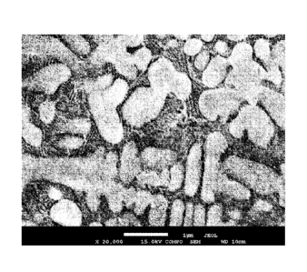
FIGS. 8 and 9 show SEM images of Alloy A5 and A6, respectively, produced via
PBF-L
after heat treating for 8 hr at 1100 C. The dark secondary boride phases have
clearly
transformed to a spheroidized structure and grown from the initial shape and
size, as seen in
FIGS. 3 and 4.
FIGS. 10 and 11 show SEM micrographs and the EDS spectra of PBF-L processed
alloys
A5 and A6, respectively, after heat treating for 8 hr at 1100 C. The EDS
spectra in FIGS. 10 and
11 show very well defined boron peaks in the dark phase of Spectrum 1 and no
boron peak in the
light phase of Spectrum 2.
FIGS. 12 and 13 show (a) SEM images and elemental maps of the PBF-L processed
alloys A5 and A6, respectively, heat treated at 1100 C for 8 hr, for the
primary elements (b) iron,
(c) nickel, (d) silicon, (e) boron, (f) chromium, (g) oxygen, and (h) Mn,
contained within the
various phases where applicable. The elemental map was generated with energy-
dispersive
9
CA 03003905 2018-05-01
WO 2017/079351 PCT/US2016/060185
spectroscopy in a Jeol JSM-7001F Field Emission SEM and Oxford Inca EDS System
with an
accelerating voltage of 4keV, probe current of 14i1A, and livetime of 240 s.
The map shows that
the secondary phases are largely enriched in boron, chromium, and oxygen, and
the primary
matrix phase is enriched in Fe, Ni, Si, and Mn. Comparing the elemental maps
of the pre- heat
treated alloys in FIG. 6 and FIG. 7 with the maps of the post-heat treated
alloys in FIGS 12 and
13, it is seen that the elements that make up the secondary boride phases are
depleted from the
matrix phase and have enriched the secondary phases.
FIG. 14 shows micrographs of alloy A6 processed via PBF-L in the (a) as-built,
(b) heat
treated at 1100 C for 3 hr, and (c) heat treated at 1100 C for 8 hr,
conditions. The boride phases
clearly grow with increasing time at the high temperature, indicating that the
growth is via
diffusion.
Table 1 shows the tensile elongation, impact toughness, and abrasion
resistance values
for PBF-L processed alloys A5, A6, and A7 in as-built and heat treated (1100 C
for 8hr)
conditions. The tensile elongation and impact toughness are measures of
material toughness.
The tensile specimens were measured per ASTM E8-13a, the un-notched impact
toughness was
measured per ASTM E23-12c(2012), and the wear resistance (volume loss) was
measured by
ASTM G65-04(2010) Procedure A. Heat treating can be seen to increase the
tensile elongation,
impact toughness, and abrasion resistance. Heat treating the layer-by-layer
constructed materials
has increased the abrasion resistance by a factor of 2.8 in alloy A5, by a
factor of 3.6 in alloy A6,
and by a factor of 2.6 in alloy A7, and increased the elongation by a factor
of 2.7 in alloy A5, by
a factor of 34.5 in alloy A6, and by a factor of 14.7 in alloy A7.
Table 1: Effect of heat treating on impact toughness and wear resistance
properties of PBF-
L layer-by-layer constructed alloys of the present invention
As Built Heat Treated
Alloy
Tensile Impact Abrasion Tensile Impact Abrasion
Elongation Toughness Resistance Elongation Toughness Resistance
CA 03003905 2018-05-01
WO 2017/079351 PCT/US2016/060185
[Vc] [J] [mm3] 11(70] [J]
[Mal3]
A5 5.2 27 432 14.1 119 157
A6 0.4 28 410 13.8 146 115
A7 1.7 22 412 25.4 114 160
Table 2 show a comparison of the tensile elongation, impact toughness, and
abrasion
resistance properties of PBF-L heat treated alloys of exemplary examples of
alloys of the present
invention and conventional alloys used in PBF-L. The tensile elongation was
measured per
ASTM E8-13a, the impact toughness was measured per ASTM E23-12c(2012) and the
abrasion
resistance was measured per ASTM G65-04(2010) Procedure A. Unnotched impact
toughness
specimens were used in the measurements except where indicated otherwise.
Table 2: Impact toughness and wear resistance properties of PBF-L layer-by-
layer
constructed alloys of the present invention and conventional alloys
Abrasion Tensile Impact
Material Type Grade Heat Treatment Resistance Elongation
Toughness
[mm] [Vc] [J]
Stainless Steel Alloy AS 1100 C for 8 hr 157
14.1 119
Stainless Steel Alloy A6 1100 C for 8 hr 115
13.8 146
Stainless Steel Alloy A7 1100 C for 8 hr 160
25.4 114
Stainless Steel 17-4PH H900 300 13.8 234
Stainless Steel 316L 388 C for 5 hr 346 28.2
99.0*
Steel 18Ni 300 491 C for 6 hr 410
4.2 107
Steel H13 580 C for 1 hr (x2) 191 0.5 3*
*Charpy v-notch specimens
While preferred embodiments of the present disclosure has been described, it
should be
understood that various changes, adaptations and modifications can be made
therein without
departing from the spirit of the disclosure and the scope of the appended
claims. The scope of
11
CA 03003905 2018-05-01
WO 2017/079351 PCT/US2016/060185
the disclosure should, therefore, be determined not with reference to the
above description, but
instead should be determined with reference to the appended claims along with
their full scope of
equivalents.
12