Note: Claims are shown in the official language in which they were submitted.
47
CLAIMS
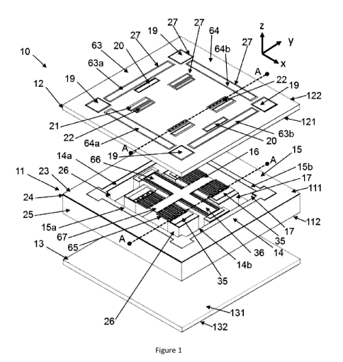
1. A three-dimensional (3D) micro-electro-mechanical system (MEMS)
magnetometer
(10) for measuring first, second and third magnetic field components
respectively
along mutually orthogonal first, second and third axes, the 3D MEMS
magnetometer
(10) comprising:
- a MEMS wafer (11) having opposed top and bottom sides (111, 112), the
MEMS wafer (11) comprising a frame structure (17) and current-carrying first,
second and third magnetic field transducers (14, 15, 16);
- a top cap wafer (12) and a bottom cap wafer (13) respectively bonded to
the
top side (111) and the bottom side (112) of the MEMS wafer (11), the top cap
wafer (12), the bottom cap wafer (13) and the MEMS wafer (11) being
electrically conductive and stacked one on top of the other along the third
axis,
the top cap wafer (12), the bottom cap wafer (13) and the frame structure (17)
together forming one or more cavities (32), each cavity (32) enclosing at
least
one of the first, second and third magnetic field transducers (14, 15, 16),
each
magnetic field transducer (14, 15, 16) being enclosed in one of the one or
more
cavities (32); and
- first, second and third electrode assemblies (63, 64, 65), the first and
second
electrode assemblies (63, 64) each being formed in either or both of the top
and bottom cap wafers (12, 13), each of the first, second and third electrode
assemblies (63, 64, 65) being configured to sense an output of a respective
one of the first, second and third magnetic field transducers (14, 15, 16)
induced by a respective one of the first, second and third magnetic field
components.
2. The 3D MEMS magnetometer (10) according to claim 1, wherein each of the
first,
second and third electrode assemblies (63, 64, 65) is configured to
capacitively sense
48
a displacement of the respective one of the first, second and third magnetic
field
transducers (14, 15, 16) in response to a Lorentz force produced by the
respective
one of the first, second and third magnetic field components.
3. The 3D MEMS magnetometer (10) according to claim 2, wherein the first and
second magnetic field transducers (14, 15) are suspended from the frame
structure (17), configured to carry a current along the second and first axes,
respectively, and deflectable along the third axis in response to the Lorentz
force
produced by the first and second magnetic field components, respectively.
4. The 3D MEMS magnetometer (10) according to claim 3, wherein the first
magnetic
field transducer (14) comprises a first pair of elongated transducer elements
(14a,
14b) extending along the second axis, and wherein the second magnetic field
transducer (15) comprises a second pair of elongated transducer elements (15a,
15b)
extending along the first axis.
5. The 3D MEMS magnetometer (10) according to claim 4, wherein:
- the first pair of elongated transducer elements (14a, 14b) are configured
to
carry equal and opposite currents;
- the first electrode assembly (63) forms a first pair of capacitors with
the first
pair of elongated transducer elements (14a, 14b) and is configured to measure
a first differential capacitance between the first pair of capacitors, the
first
differential capacitance being indicative of a magnitude of the first magnetic
field component;
- the second pair of elongated transducer elements (15a, 15b) are
configured to
carry equal and opposite currents; and
- the second electrode assembly (64) forms a second pair of capacitors with
the
second pair of elongated transducer elements (15a, 15b) and is configured to
49
measure a second differential capacitance between the second pair of
capacitors, the second differential capacitance being indicative of a
magnitude
of the second magnetic field component.
6. The 3D MEMS magnetometer (10) according to any one of claims 1 to 5,
wherein
each of the first and second electrode assemblies (63, 64) comprises one or
more
sense electrodes (63a, 63b, 64a, 64b), each sense electrode (63a, 63b, 64a,
64b)
being laterally bordered by an insulating closed-loop trench (27) extending
along the
third axis and at least partially into the either one of the top and bottom
cap wafers
(12, 13).
7. The 3D MEMS magnetometer (10) according to any one of claims 1 to 6,
wherein
the third magnetic field transducer (16) comprises a stationary transducer
element (35) and a movable transducer element (36) respectively fixed and
displaceable in a plane perpendicular to the third axis relative to the frame
structure (17), the movable transducer element (36) being configured to carry
a
current in said plane.
8. The 3D MEMS magnetometer (10) according to claim 7, wherein the third
electrode
assembly (65) is configured to capacitively sense a relative motion between
the
stationary transducer element (35) and the movable transducer element (36),
said
relative motion being indicative of a magnitude of the third magnetic field
component.
9. The 3D MEMS magnetometer (10) according to claim 8, wherein the third
electrode
assembly (65) forms an interdigitated capacitive structure comprising at least
one first
set of conductive digits (38, 39) provided on the stationary transducer
element (35)
and at least one second set of conductive digits (37) provided on the movable
transducer element (36), the at least one first set and the at least one
second set of
50
conductive digits (37, 38, 39) being interlocked and capacitively coupled with
each
other.
10. The 3D MEMS magnetometer (10) according to any one of claims 1 to 9,
wherein
the third electrode assembly (65) is formed in the MEMS wafer (11).
11. The 3D MEMS magnetometer (10) according to claim 10, further comprising:
- one or more electrical contacts (46) formed on an outer side (122) of the
top
cap wafer (12); and
- an electrically conductive path (70) extending across and through the top
cap
wafer (12) to electrically connect the one or more electrical contacts (46) to
the
third electrode assembly (65).
12. The 3D MEMS magnetometer (10) according to any one of claims 1 to 11,
wherein the top cap wafer (12), the bottom cap wafer (13) and the MEMS wafer
(11)
are each made at least partially of silicon-based material.
13. The 3D MEMS magnetometer (10) according to any one of claims 1 to 12,
wherein the MEMS wafer (11) is a silicon-on-insulator wafer comprising a MEMS
device layer (23) bonded to the top cap wafer (12), a MEMS handle layer (25)
bonded
to the bottom cap wafer (13), and a MEMS insulating layer (24) interposed
between
the MEMS device layer (23) and the MEMS handle layer (25).
14. The 3D MEMS magnetometer (10) according to any one of claim 1 to 13,
wherein
at least one of the top cap wafer (12) and the bottom cap wafer (13) is a
silicon-on-
insulator wafer including a cap device layer (60), a cap handle layer (62),
and a cap
insulating layer (61) interposed therebetween.
51
15. The 3D MEMS magnetometer (10) according to any one of claims 1 to 14,
wherein at least one of the one or more cavities (32) is a hermetically sealed
vacuum
cavity.
16. The 3D MEMS magnetometer (10) according to any one of claims 1 to 15,
wherein the one or more cavities (32) consist of a single cavity enclosing the
first,
second and third magnetic field transducers (14, 15, 16).
17. The 3D MEMS magnetometer (10) according to any one of claims 1 to 16,
wherein the first, second and third magnetic field transducers (14, 15, 16)
form
respective first, second and third resonant structures having associated
resonant
frequencies, each of the first, second and third magnetic field transducers
configured
to carry current at a frequency matching the resonant frequency associated
thereto.
18. A 3D MEMS magnetometer (10) for measuring first, second and third magnetic
field components respectively along mutually orthogonal first, second and
third axes,
the 3D MEMS magnetometer (10) comprising:
- a MEMS wafer (11) having opposed top and bottom sides (111, 112), the
MEMS wafer (11) comprising a frame structure (17) and current-carrying first,
second and third magnetic field transducers (14, 15, 16), the MEMS wafer (11)
being a silicon-on-insulator wafer with a MEMS device layer (23), a MEMS
handle layer (25), and a MEMS insulating layer (24) interposed between the
MEMS device layer (23) and the MEMS handle layer (25), the first, second and
third magnetic field transducers (14, 15, 16) being formed in the MEMS device
layer (25);
- a top cap wafer (12) and a bottom cap wafer (13) respectively bonded to the
MEMS device layer (25) and the MEMS handle layer (25), the top cap
wafer (12), the bottom cap wafer (13) and the MEMS wafer (11) being
52
electrically conductive and stacked one on top of the other along the third
axis,
the top cap wafer (12), the bottom cap wafer (13) and the frame structure (17)
together forming one or more cavities (32), each cavity (32) enclosing at
least
one of the first, second and third magnetic field transducers (14, 15, 16),
each
magnetic field transducer (14, 15, 16) being enclosed in one of the one or
more
cavities (32); and
- first, second and third electrode assemblies (63, 64, 65), the first and
second
electrode assemblies (63, 64) each being formed in the top cap wafer (12),
each of the first, second and third electrode assemblies (63, 64, 65) being
configured to sense an output of a respective one of the first, second and
third
magnetic field transducers (14, 15, 16) induced by a respective one of the
first,
second and third magnetic field components.
19. The 3D MEMS magnetometer (10) according to claim 18, wherein the top cap
wafer (12) is a silicon-on-insulator wafer comprising a top cap device layer
(60)
bonded to the MEMS device layer (23), a top cap handle layer (62), and a top
cap
insulating layer (61) interposed between the top cap device layer (60) and the
top cap
handle layer (62).
20. The 3D MEMS magnetometer (10) according to claim 19, wherein each of the
first
and second electrode assemblies (63, 64) is etched in the top cap device layer
(60).
21. The 3D MEMS magnetometer (10) according to claim 20, wherein the top cap
wafer (12) includes recesses (30) formed therein and defining capacitor gaps
(31)
between the first electrode assembly 63 and the first magnetic field
transducer (14),
and between the second electrode assembly 64 and the second magnetic field
transducer (15).
53
22. The 3D MEMS magnetometer (10) according to claim 21, further comprising:
- at least one first electrical contact (46a) formed on an outer side of
the top cap
handle layer (62), and a first electrically conductive path (70a) extending
across and successively through the top cap handle, insulating and device
layers (62, 61, 60) to electrically connect the at least one first electrical
contact (46a) to the first electrode assembly (63); and
- at least one second electrical contact (46b) formed on an outer side of
the top
cap handle layer (62), and a second electrically conductive path (70b)
extending across and successively through the top cap handle, insulating and
device layers (62, 61, 60) and to electrically connect the at least one second
electrical contact (46b) to the second electrode assembly (64).
23. The 3D MEMS magnetometer (10) according to any one of claims 18 to 22,
wherein the third electrode assembly (65) is formed in the MEMS device layer
(23).
24. The 3D MEMS magnetometer (10) according to claim 23, further comprising:
- at least one third electrical contacts (46) formed on an outer side (122)
of the
top cap wafer (12); and
- an third electrically conductive path (70) extending across and through
the top
cap wafer (12) to electrically connect the at least one third electrical
contacts (46) to the third electrode assembly (65).
25. The 3D MEMS magnetometer (10) according to any one of claims 18 to 24,
wherein each of the first, second and third electrode assemblies (63, 64, 65)
is
configured to capacitively sense a displacement of the respective one of the
first,
second and third magnetic field transducers (14, 15, 16) in response to a
Lorentz
force produced by the respective one of the first, second and third magnetic
field
components.
54
26. The 3D MEMS magnetometer (10) according to claim 25, wherein the first and
second magnetic field transducers (14, 15, 16) are suspended from the frame
structure (17), configured to carry a current along the second and first axes,
respectively, and deflectable along the third axis in response to the Lorentz
force
produced by the first and second magnetic field components, respectively.
27. The 3D MEMS magnetometer (10) according to claim 26, wherein the first
magnetic field transducer (14) comprises a first pair of elongated transducer
elements (14a, 14b) extending along the second axis, and wherein the second
magnetic field transducer (15b) comprises a second pair of elongated
transducer
elements (15a, 15b) extending along the first axis.
28. The 3D MEMS magnetometer (10) according to claim 27, wherein:
- the first pair of elongated transducer elements (14a, 14b) are configured
to
carry equal and opposite currents;
- the first electrode assembly (63) forms a first pair of capacitors with
the first
pair of elongated transducer elements (14a, 14b) and is configured to measure
a first differential capacitance between the first pair of capacitors, the
first
differential capacitance being indicative of a magnitude of the first magnetic
field component;
- the second pair of elongated transducer elements (15a, 15b) are
configured to
carry equal and opposite currents; and
- the second electrode assembly (64) forms a second pair of capacitors with
the
second pair of elongated transducer elements (15a, 15b) and is configured to
measure a second differential capacitance between the second pair of
capacitors, the second differential capacitance being indicative of a
magnitude
of the second magnetic field component.
55
29. The 3D MEMS magnetometer (10) according to any one of claims 18 to 28,
wherein each of the first and second electrode assemblies (63, 64) comprises
one or
more sense electrodes (63a, 63b, 64a, 64b), each sense electrode (63a, 63b,
64a,
64b) being laterally bordered by an insulating closed-loop trench (27)
extending along
the third axis and at least partially into the top cap wafer (12).
30. The 3D MEMS magnetometer (10) according to any one of claims 18 to 29,
wherein the third magnetic field transducer (65) comprises a stationary
transducer
element (35) and a movable transducer element (36) respectively fixed and
displaceable in a plane perpendicular to the third axis, the movable
transducer
element (36) being configured to carry a current along at said plane.
31. The 3D MEMS magnetometer (10) according to claim 30, wherein the third
electrode assembly (65) is configured to capacitively sense a relative motion
between
the stationary transducer element (35) and the movable transducer element
(36), said
relative motion being indicative of a magnitude of the third magnetic field
component.
32. The 3D MEMS magnetometer (10) according to claim 31, wherein the third
electrode assembly (65) forms an interdigitated capacitive structure
comprising at
least one first set of conductive digits (38, 39) provided on the stationary
transducer
element (35) and at least one second set of conductive digits (37) provided on
the
movable transducer element (36), the at least one first set and the at least
one
second set of conductive digits (37, 38, 39) being interlocked and
capacitively
coupled with each other.
33. The 3D MEMS magnetometer (10) according to any one of claims 18 to 32,
wherein at least one of the one or more cavities (32) is a hermetically sealed
vacuum
cavity.
56
34. The 3D MEMS magnetometer (10) according to any one of claims 18 to 33,
wherein the one or more cavities (32) consist of a single cavity enclosing the
first,
second and third magnetic field transducers (14, 15, 16).
35. A method for measuring first, second and third magnetic field components
along
mutually orthogonal first, second and third axes, respectively, the method
comprising:
- providing a 3D MEMS magnetometer (10) comprising a MEMS wafer (11)
having opposed top and bottom sides, the MEMS wafer (11) comprising a
frame structure and current-carrying first, second and third magnetic field
transducers, a top cap wafer (12) and a bottom cap wafer (13) respectively
bonded to the top side and the bottom side of the MEMS wafer (11), the top
cap wafer (12), the bottom cap wafer (13) and the MEMS wafer (11) being
electrically conductive and stacked one on top of the other along the third
axis,
the top cap wafer (12), the bottom cap wafer (13) and the frame structure (17)
together forming one or more cavities (32), each cavity (32) enclosing at
least
one the first, second and third magnetic field transducers (14, 15, 16), each
magnetic field transducer (14, 15, 16) being enclosed in one of the one or
more
cavities (32);
- flowing current into each of the first, second and third magnetic field
transducers (14, 15, 16); and
- sensing an output of each the first, second and third magnetic field
transducers (14, 15, 16) induced by and indicative of a respective one of the
first, second and third magnetic field components.
36. The method according to claim 35, comprising:
57
- flowing a first current into the first magnetic field transducer (14),
the first
magnetic field transducer (14) being deflectable along the third axis and
configured to carry the first current along the second axis;
- sensing, as a first capacitance, a deflection of the first magnetic field
transducer (14) along the third axis in response to a first Lorentz force
resulting
from an interaction between the first current and the first magnetic field
component, the first capacitance being indicative of a magnitude of the first
magnetic field component;
- flowing a second current into the second magnetic field transducer (15),
the
second magnetic field transducer (15) being deflectable along the third axis
and configured to carry the second current along the first axis;
- sensing, as a second capacitance, a deflection of the second magnetic
field
transducer (15) along the third axis in response a second Lorentz force
resulting from an interaction between the second current and the second
magnetic field component, the second capacitance being indicative of a
magnitude of the second magnetic field component;
- flowing a third current into a movable transducer element (36) of the
third
magnetic field transducer (16), the movable transducer element (36) being
displaceable relative to a stationary transducer element (35) of the third
magnetic field transducer (16) and configured to carry the third current in a
plane perpendicular to the third axis; and
- sensing, as a third capacitance, a relative motion between the stationary
and
movable transducing elements (35, 36) in said plane, the third capacitance
being indicative of a magnitude of the third magnetic field component.