Note: Descriptions are shown in the official language in which they were submitted.
CA 03005098 2018-05-11
WO 2016/074044 PCT/AU2015/050712
1
ELECTRICAL GENERATOR SYSTEM
Technical Field
[0001] The present invention relates to the field of electrical generation,
and in
particular, to electrical energy converted from the energy from radioactive
emissions.
Background of the Invention
[0002] Power cells provide a self-contained source of electrical energy for
driving an
external load. A common example of an electrical power cell is an
electrochemical battery.
While electrochemical batteries are effective at providing power needs for a
period of time
at a relatively low cost, the limiting factor is the available energy defined
by the material
type and weight. Due to the limited energy storage and energy density of
electrochemical
batteries with regard to their mass, there have been various attempts at
producing
alternative power cells, such as batteries powered by radioactive isotopes due
to the
higher theoretical limits of energy density.
[0003] There are several different types of radioisotope-powered batteries.
Once such
type is a radio thermal generator (RTG) which uses the heat produced during
decay of
radioactive material to produce electrical energy. These devices have low
conversion
efficiency of the heat energy to electrical energy. Accordingly, RTGs are
generally used
with very high energy radioisotopes to produce a source of electrical power
and usually
require substantial shielding. In addition, the electrical power output is
low.
[0004] Another type of radioisotope-powered battery is an indirect
conversion device
which uses a radioisotope, luminescent material and a photovoltaic cell. The
decay
particles emitted by the radioisotope excite the luminescent material. The
light emitted by
the luminescent material is absorbed by the photovoltaic cells to generate
electricity. This
type of battery generally has low efficiency because of the two step
conversion and a
relatively short lifespan because the luminescent material is damaged by the
emissions.
[0005] Another example of a radioisotope powered battery is a direct
conversion
device which uses a radioisotope and semiconducting material. Conventional
semiconductors are of only limited use in this application, as they suffer
collateral
radiation damage from the radioisotope decay products. In particular, incident
high-
energy beta particles create defects in the semiconductor that scatter and
trap the
generated charge carriers. The damage accumulates and thereby over time
reduces the
performance of the battery.
CA 03005098 2018-05-11
WO 2016/074044 PCT/AU2015/050712
2
[0006] US 5,260,621 discloses a solid state nuclear battery comprising a
relatively
high energy radiation source, with concomitant heat generation, and a bulk
crystalline
semiconductor such as AIGaAs, which is characterised by defect generation in
response
to the radioisotope. The material is chosen so that radiation damage is
repaired by
annealing at the elevated operating temperature of the battery. This device
suffers from
low efficiency, which necessitates the use of a high energy radiation source
and also
requires elevated operating temperatures to function.
[0007] US 5859484 teaches a solid state radioisotope-powered semiconductor
battery comprising a substrate of crystalline semiconductor material such as
GalnAsP.
This battery preferably uses a radioisotope that emits only low energy
particles to
minimise degradation of the semiconductor material in order to maximise
lifetime. The
effect of using a lower energy radiation source is a lower maximum power
output.
[0008] A further such device is disclosed in US 6479919, which describes a
beta cell
incorporating icosahedral boride compounds, for example B12P2 or B12As2, a
beta
radiation source and a means for transmitting electrical energy to an outside
load.
Manufacturing boron arsenide and boron phosphide is expensive, which increases
the
cost of producing these types of devices. Further, the production of such
devices has
increased health, safety and environmental risks associated with handling the
arsenide
and phosphide materials.
[0009] In summary, problems with currently available radioisotope powered
cells
include inefficiency of conversion of the emitted energy to electrical energy,
radiation
damage affecting the device materials, shielding requirements for high energy
nuclear
sources and semiconductor material that is subject to degradation.
[0010] It is an object of the present invention to provide a radioisotope
power cell
which exhibits an improved balance between durability and power output.
Summary of the Invention
[0011] According to the present invention there is provided an electrical
generator
system including: a radionuclide material; a thin layer of zinc oxide; metal
electrodes
contacting the zinc oxide and forming a metal-semiconductor junction
therebetween,
wherein radioactive emissions received from the radionuclide material are
converted into
electrical energy at the metal-semiconductor junction; and electrical contacts
connected
to the electrodes which facilitate the flow of the electrical energy when
connected to a
load.
CA 03005098 2018-05-11
WO 2016/074044 PCT/AU2015/050712
3
[0012] The use of zinc oxide was found by the inventors to have surprising
results.
While zinc oxide is an intrinsic n-type semiconductor, it has limited or no
commercial
applications as a semi-conductor material due to the lack of stable doped p-
type ZnO
materials. Consequently, it is considered a poor choice of semiconductor
material for
forming p-n junctions, which has been the primary direction for structuring
radioisotope
powered cells.
[0013] Traditionally accepted choices of semiconductor materials, such as
GaAs,
GalnAs; or Si, Si-C; or CdTe; etc, have been found to structurally degrade
when exposed
to high levels of radiation.
[0014] The inventor has discovered that zinc oxide, when employed at an
appropriate
thickness, could withstand high radiation levels and could, when employed as
part of a
metal-semiconductor junction (as opposed to a p-n junction), give favourable
electrical
generation output.
Brief Description of the Drawings
[0015] Embodiments of the present invention will now be described with
reference to
the accompanying drawings, in which:
[0016] Fig. 1 is a graph showing the variation in generated current with
the variation
in zinc oxide thickness in tests with an applied voltage of 3V;
[0017] Fig. 2 is a graph showing the variation in generated current with
the variation
in zinc oxide thickness with different electrode materials and configurations
in tests with
an applied voltage of 3V;
[0018] Fig. 3 is a graph showing variation of generated current against
applied voltage
with varying distance of radionuclide from the zinc oxide layer;
[0019] Fig. 4 is schematic view of a first embodiment of a power supply
device;
[0020] Fig. 5 is a schematic of an alternative embodiment of a power supply
device;
[0021] Fig. 6 is a schematic of a further alternative embodiment of a power
supply
device.
CA 03005098 2018-05-11
WO 2016/074044 PCT/AU2015/050712
4
Detailed Description of the invention
[0022] The present invention will be principally described with reference
to particular
illustrative examples. It will be understood that the principles of the
present invention may
be implemented using variations of features on the particular implementations
illustrated
and described. The examples should be considered as illustrative and not
!imitative of
the broad inventive concepts disclosed herein.
[0023] One implementation of the present invention is an electrical
generation system
employing an n-type semiconductor material having metal electrodes in contact
with the
semiconductor material, and exposing the arrangement to radiation from a
radionuclide
material. The radioactive emissions are converted into electrical energy at
the metal-
semiconductor junction formed between the electrodes and the semiconductor
material.
For flow of generated electrical energy, it is important that there is a
potential difference
between the electrodes. Hence, there needs to be a significant difference in
metal to
semiconductor contact area between the electrodes in order that greater charge
generation is created at one electrode compared with the other. The electrode
having
greater charge accumulation effectively becomes the negative terminal and the
other
electrode becomes the positive terminal.
[0024] To maximise electrical generation in a radioisotope power cell, it
is desirable
to use a relatively high energy level radiation source and a high activity
density. However,
most semiconductor materials cannot withstand such high energy levels and
structurally
degrade with exposure.
[0025] Zinc oxide is an n-type semiconductor, but is dismissed in the field
as being a
very poor semiconductor material. However, the present inventor has discovered
that
zinc oxide does demonstrate a capacity to withstand relatively high energy
levels of
radiation and high activity density.
[0026] Initial tests employing zinc oxide in the proposed electrical
generation system
unfortunately gave the disappointing results predicted by the accepted opinion
in the field,
which was that ZnO is a poor semiconductor material. Despite the capacity to
withstand
high levels of radiation, the generated electrical output was negligible.
[0027] However, when tests were conducted on varying the thickness of zinc
oxide
employed in the proposed electrical generation system, surprisingly favourable
results
were found when the zinc oxide was provided in the form of a sufficiently thin
layer or film.
For the purposes of the present description and claims, 'thin' means less than
about
15 m, and preferably less than10 m.
CA 03005098 2018-05-11
WO 2016/074044 PCT/AU2015/050712
[0028] Figure 1 is a graph showing the variation in generated current with
the variation
in zinc oxide thickness in tests with an applied voltage of 3V. In this test,
the optimal
current was at 1000 nm.
[0029] In practical experiments, a thin film of zinc oxide was formed on a
substrate,
by rf magnetron sputter or electrochemical vapour deposition, having a 5cm x
5cm
surface. The substrate consisted of a first layer of glass. In this regard,
sapphire and
quartz are also considered suitable for this first layer. The substrate
further consisted of
a layer of a doped metal oxide material, which formed the surface upon which
the zinc
oxide was deposited.
[0030] This layer of a doped metal oxide material allowed the smaller
positive
electrode to be formed thereupon, thereby separating the positive electrode
from the zinc
oxide but providing a current path due to the semiconductive properties of the
doped
metal oxide. Suitable doped metal oxide materials include, but are not limited
to, fluorine
doped tin oxide and tin-doped indium oxide.
[0031] A number of metal materials were tested for suitability as
electrodes, namely
gold, copper, aluminium and silver. In addition, different electrode
configurations were
examined, a first whereby the electrode covered an entire surface of the zinc
oxide layer
and a second whereby a comb-like or finger-like grid formation was used on the
zinc oxide
surface. The general thickness of the metal electrode material was in the
range of 100-
1000nm, and preferably 150 nm.
[0032] Gold and copper were deposited by using sputtering techniques, while
aluminium and silver were deposited using thermal evaporation techniques.
[0033] The different samples were exposed to Sr-90. Results found that
gold,
aluminium and silver produced linear and symmetric current-voltage curves at
the metal-
semiconductor junction suggesting a desirable degree of ohmic contact between
these
metals and the zinc oxide.
[0034] Copper produced non-linear and asymmetric results, indicative of a
Schottky
barrier, which suggests that it is unsuitable for the present purposes.
[0035] In respect of the different configurations, a negligible difference
in results was
noted. This suggests that the comb-like grid configuration, which uses less
metal, is a
viable option. It will be appreciated that other geometries and configurations
are
contemplated within the scope of the present invention.
CA 03005098 2018-05-11
WO 2016/074044 PCT/AU2015/050712
6
[0036] Similarly, it will be understood that the present invention could be
implemented
with different metals, including alloys, in the metal-semiconductor junction.
[0037] Tests were conducted with different thicknesses of the zinc oxide
layer
between 150nm and 1500nm.
[0038] The surprising results found that as thickness increased from 150nm
the
generated electrical output also increased until an optimum thickness, after
which,
increasing the thickness caused a reduction in generated electrical output.
Beyond
approximately 1500nm, the output became too low for practical purposes.
Consequently,
the tests suggested an ideal thickness range for the zinc oxide to be between
150nm and
1500nm. The optimum thickness did vary depending upon selection of materials.
[0039] The optimum thickness did vary depending upon selection of
materials. Figure
2 illustrates the variation in current with thickness at a constant voltage
and radiation
source, but with different materials and thicknesses of material. The material
included
silver in a finger electrode configuration; silver in full electrode;
aluminium in a finger
electrode configuration; aluminium in full coverage; and gold in full
coverage.
[0040] In certain tests the optimum thickness was 1000nm while in other
tests the
optimum thickness was 1250nm, see Figs 1 and 2. Nevertheless, the overall
useful range
of thicknesses stayed reasonably constant. It is expected that the optimum
thickness
could also vary, within the range, depending upon the choice of radionuclide
material.
[0041] Alternative beta emitting materials which could be used in
implementations of
the present invention include Pm-147, Ni-63 and Tritium, or any other suitable
beta
emitting material. The present invention is in principle able to use other
kinds of
radioactive material, for example x-ray sources, gamma sources, or any other
suitable
material. The radionuclides may be in any suitable chemical form, and the
material could
in principle be a mixture of different radionuclide or with other materials.
[0042] Tests were also conducted on varying the distance and angle of
incidence of
the Sr-90 material to the zinc oxide layer, varying between 2mm and 350mm,
shown in
figure 3. Figure 3 is a graph showing variation of generated current against
applied
voltage, with varying distances of the radionuclide from the zinc oxide layer.
[0043] As expected, the best output occurred at the smallest distance with
output
decreasing as distance was increased. Nevertheless there was still appreciable
output
throughout the tested range, particularly up to approximately 300mm and an
angle of
CA 03005098 2018-05-11
WO 2016/074044 PCT/AU2015/050712
7
<45 . Given the thickness dimensions of the generator, this is a large space
and
suggested that a number of generator arrangements could be arranged in a
layered
structure with the same radionuclide material, thereby increasing the
electrical output
capacity from a single radionuclide source.
[0044] Examples of power supply devices employing the electrical generator
system
will now be described.
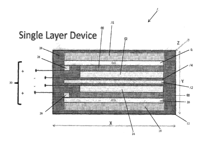
[0045] In Fig. 4 there is shown a basic 'single layer' device 10. As shown,
the device
includes a housing 12, within which at its centre is a layer of a sealed
radionuclide 14,
for example, Sr-90, Pm-147, Ni-63 or H-3. The housing 12 can be formed of
various
suitable materials, such as aluminium, steel, etc., and encloses an atmosphere
of air 28.
The seal 16 can be aluminium, plastic, Mylar, other suitable metal alloy or
similar low Z-
material (Z being atomic weight). On each side of the radionuclide 14 are
substrates 18
(for example, glass substrates) having a layer of tin-doped indium oxide 20
and a thin
layer of zinc oxide 22 formed thereupon. An alternative to tin-doped indium
oxide can be
indium tin fluoride. The main negative electrode 24 is formed on the other
surface of the
zinc oxide 22 and the smaller positive electrode 26 is formed on a surface of
the tin-doped
indium oxide 20. Conductive leads 30 are connected to both electrodes 24, 26
and lead
to exterior of the housing 12 for connection to a load.
[0046] In Fig 5 there is a shown a 'double layer' device 110. Each side of
the central
radionuclide 114 has an arrangement of two zinc oxide layers 122, each with
corresponding electrodes 124, 126, doped metal oxide layers 120 and separated
by an
insulating substrate 132.
[0047] In Fig. 6 there is shown a 'triple layer' device 210, in which
layers of substrate
and ZnO are arranged in a sandwich arrangement. Similarly to the other
examples, a
central sealed radionuclide 214 has an arrangement of 3 layers of substrate
232 either
side, with ZnO layers 222, doped metal oxide layers 220 and electrodes 224,
226.
[0048] As will be appreciated, it is possible to keep increasing the number
of layers
and, as a consequence, increase generated electrical output. The limit to how
many
layers can be employed is dictated by how far away from the radionuclide
material the
furthest layer is.
[0049] It will be appreciated that structures with more than one layer of
radionuclide
may be used, with multiple sandwich structures added to provide a desired
power level.
It will also be understood that although the structure described is generally
square in
CA 03005098 2018-05-11
WO 2016/074044 PCT/AU2015/050712
8
shape, the structure could be of any desired shape, and could be curved in a
suitable
implementation, assuming appropriate spacings can be maintained.