Note: Descriptions are shown in the official language in which they were submitted.
CA 03005273 2018-05-11
SENSOR INTERROGATION WITH FAST RECOVERY
[01]
BACKGROUND
[02] The following information is provided to assist the reader in
understanding
technologies disclosed below and the environment in which such technologies
may typically
be used. The terms used herein are not intended to be limited to any
particular narrow
interpretation unless clearly stated otherwise in this document. References
set forth herein
may facilitate understanding of the technologies or the background thereof.
The disclosure of
all references cited herein may be referred to.
[03] Prudence dictates that gas detection instrumentation be tested
regularly for
functionality. It is a common practice to, for example, perform a "bump
check," or
functionality check on portable gas detection instrumentation on a daily
basis. The purpose of
this test is to ensure the functionality of the entire gas detection system,
commonly referred to
as an instrument. A periodic bump check or functionality check may also be
performed on a
permanent gas detection instrument to, for example, extend the period between
full
calibrations. Gas detection systems include at least one gas sensor,
electronic circuitry and a
power supply to drive the sensor, interpret its response and display its
response to the user.
The systems further include a housing to enclose and protect such components.
A bump
check typically includes: a) applying a gas of interest (usually the target
gas or analyte gas the
instrument is intended to detect); b) collecting and interpreting the sensor
response; and
c) indicating to the end user the functional state of the system (that is,
whether or not the
instrument is properly functioning).
[04] Such bump tests are performed regularly and, typically, daily. Bump
checks
provide a relatively high degree of assurance to the user that the gas
detection device is
working properly. The bump check exercises all the necessary functionalities
of all parts of
the gas detection device in the same manner necessary to detect an alarm level
of a hazardous
gas. In that regard, the bump check ensures that there is efficient gas
delivery from the
outside of the instrument, through any transport paths (including, for
example, any protection
CA 03005273 2018-05-11
WO 2017/136407 PCT/US2017/015985
and/or diffusion membranes) to contact the active sensor components. The bump
check also
ensures that the detection aspect of the sensor itself is working properly and
that the sensor
provides the proper response function or signal. The bump check further
ensures that the
sensor is properly connected to its associated power supply and electronic
circuitry and that
the sensor signal is being interpreted properly. Moreover, the bump check
ensures that the
indicator(s) or user interface(s) (for example, a display and/or an
annunciation functionality)
of the gas detection instrument is/are functioning as intended.
1051 However, a
periodic/daily bump check requirement has a number of significant
drawbacks. For example, such bump checks are time consuming, especially in
facilities such
as industrial facilities that include many gas detection systems or
instruments. The bump
check also requires the use of expensive and potentially hazardous calibration
gases. Further,
the bump check also requires a specialized gas delivery system, usually
including a
pressurized gas bottle, a pressure reducing regulator, and tubing and adapters
to correctly
supply the calibration gas to the instrument. The requirement of a specialized
gas delivery
system often means that the opportunity to bump check a personal gas detection
device is
limited in place and time by the availability of the gas delivery equipment.
1061 Recently, a number
of systems and methods have been proposed to reduce the
number of bump tests required. Such a system may, for example, include
electronic
interrogation of a sensor. A sensor is offline or unable to sense an anlayte
or target gas or
gases during such electronic interrogation. For example, a number of sensors
include
functionality to electronically interrogate of one or more electrodes thereof,
require a user to
initiate an interrogation process which takes between 20-30 seconds. For
example, a
potential change may be applied to an electrode for 5-10 seconds and the
corresponding
current decay curve is studied over a 20-30 second period. As set forth above,
during such a
20-30 second period, the sensor is offline and can't be used to sense the
analyte(s). It is
desirable to minimize the amount of time a sensor is offline, particularly in
cases wherein a
sensor is used to detect one or more hazardous analytes or target gases.
SUMMARY
107] A method of
operating a sensor to detect an analyte in an environment, wherein the
sensor includes a working electrode and circuitry in operative connection with
the working
electrode, includes performing a sensor interrogation cycle including applying
electrical
2
CA 03005273 2018-05-11
WO 2017/136407 PCT/US2017/015985
energy to the working electrode to generate a non-faradaic current, measuring
a response to
the generation of the non-faradaic current to determine a state of the sensor,
and actively
controlling the circuitry to dissipate the non-faradaic current. In a number
of embodiments,
the sensor interrogation cycle lasts less than one second. The method may, for
example,
include periodically initiating the sensor interrogation cycle.
[08] Applying electrical energy to the working electrode may, for example,
include
applying a first potential difference to the working electrode. Actively
controlling the
circuitry may, for example, include applying at least a second potential
difference to the
working electrode of opposite polarity to the first potential difference.
[09] In a number of embodiments, actively controlling the circuitry
includes decreasing
a load resistance in electrical connection with the working electrode.
Applying electrical
energy to the working electrode may, for example, include changing the
potential of the
working electrode for a period of time. The period of time may, for example,
be no greater
than 1/2 seconds, no greater than 1116 seconds, or no greater than 1/64
seconds. In a number
of embodiments, decreasing the load resistance occurs at the same time or
after measuring the
response.
[10] In a number of embodiments, the sensor comprises a load resistor and a
bypass
switch to bypass the load resistor. The bypass switch may, for example,
include a field effect
transistor switch, wherein activating a field effect transistor switch
decreases the load
resistance and deactivating the field effect transistor switch increases the
load resistance.
[11] In a number of embodiments, the method further includes adjusting the
output of
the sensor at least in part on the basis of the sensor interrogation cycle.
[12] An electrochemical sensor is operable to detect an analyte in an
environment
during an operational mode of the sensor and includes a working electrode and
circuitry in
operative connection with the working electrode, which is adapted to carry out
an electronic
interrogation cycle. The circuitry includes a power source via which
electrical energy is
applied to the working electrode during the electronic interrogation cycle to
generate a non-
faradaic current. The electrochemical sensor further includes a system to
measure a response
of the sensor and a control system to actively control the circuitry to
dissipate the non-
faradaic current. In a number of embodiments, the circuitry is adapted to
complete the sensor
3
CA 03005273 2018-05-11
WO 2017/136407 PCT/US2017/015985
interrogation cycle in less than one second. The circuitry may, for example,
be adapted to
periodically initiate the sensor interrogation cycle.
[13] The circuitry may, for example, be adapted to apply a first potential
difference to
the working electrode. The control system may, for example, actively control
the circuitry to
apply at least a second potential difference to the working electrode of
opposite polarity to
the first potential difference to dissipate the non-faradaic current. The
control system may,
for example, decrease a load resistance in electrical connection with the
working electrode to
dissipate the non-faradaic current. Decreasing the load resistance may, for
example, occur at
the same time or after measuring the response to the generation of the non-
faradaic current.
[14] Applying electrical energy to the working electrode may, for example,
include
changing the potential of the working electrode for a period of time. In a
number of
embodiments, the period of time is no greater than 1/2 seconds, no greater
than 1/16 seconds,
of no greater than 1/64 seconds.
[15] In a number of embodiments, the circuitry include a load resistor and
a bypass
switch to bypass the load resistor. The bypass switch may, for example,
include a field effect
transistor switch. Activating the field effect transistor switch may, for
example, decrease the
load resistance and deactivating the field effect transistor switch may, for
example, increase
the load resistance.
[16] In a number of embodiments, the control system is further adapted to
adjust output
of the sensor at least in part on the basis the sensor interrogation cycle.
[17] A method of operating a sensor operable to detect an analyte in an
environment,
wherein the sensor includes a working electrode and circuitry in operative
connection with
the working electrode, includes performing a sensor interrogation cycle
including applying
electrical energy to the working electrode to generate a non-faradaic current
and measuring a
response to the generation of the non-faradaic current to determine a state of
the sensor. In a
number of embodiments, the amount of energy applied is low enough in amplitude
and short
enough in duration such that the non-faradaic current dissipates quickly
enough so that a
baseline current is reached less than one second from application of the
electrical energy at
which an analytic response of the sensor can be measured to detect the
analyte.
4
CA 03005273 2018-05-11
WO 2017/136407 PCT/US2017/015985
[18] The present devices, systems, and methods, along with the attributes
and attendant
advantages thereof, will best be appreciated and understood in view of the
following detailed
description taken in conjunction with the accompanying drawings.
BRIEF DESCRIPTION OF THE DRAWINGS
[19] Figure IA illustrates schematically an embodiment of an
electrochemical sensor
hereof.
1201 Figure 1B
illustrates a schematic circuit diagram of an embodiment of a sensor
hereof.
[21] Figure 2A
illustrates recovery of a sensor signal of a sensor for hydrogen sulfide
(H28) after imposition of a 1/16th second +10mV pulse for the case in which a
load resister of
a predetermined resistance is in series with the working electrode and for the
case that the
resister is bypassed or short circuited via an FET switch at the end of the
pulse.
1221 Figure 2B
illustrates a portion of the results of Figure 2A over expanded output
and time scales.
[23] Figure 3A illustrates recovery of a sensor signal of a sensor for
hydrogen sulfide
(H2S) after imposition of a 1/64th second +10mV pulse for the case in which a
load resister of
a predetermined resistance is in series with the working electrode and for the
case that the
resister is bypassed or short circuited via an FET switch at the end of the
pulse.
[24] Figure 3B illustrates a portion of the results of Figure 3A over
expanded output
and time scales.
[25] Figure 4A illustrates recovery of a sensor signal of a sensor for
carbon monoxide
(CO) after imposition of a I/16th second +10mV pulse for the case in which a
load resister of
a predetermined resistance is in series with the working electrode and for the
case that the
resister is bypassed or short circuited via an FET switch at the end of the
pulse.
[26] Figure 4B illustrates a portion of the results of Figure 4A over
expanded output
and time scales.
CA 03005273 2018-05-11
WO 2017/136407 PCT/US2017/015985
1271 Figure 5A
illustrates recover), of a sensor signal of a sensor for carbon dioxide
after imposition of a 1/641h second +10mV pulse for the case in which a load
resister of a
predetermined resistance is in series with the working electrode and for the
case that the
resister is bypassed or short circuited via an FET switch at the end of the
pulse.
[28] Figure 5B illustrates a portion of the results of Figure 5A over
expanded time and
output scales.
[29] Figure 6 illustrates the output of a sensor hereof in response to a
+10 mV test
potential difference wherein an FET switch is activated after the measured
peak value of
output (MPV), but prior to collection of number of additional data points.
[30] Figure 7 illustrates the output of a sensor hereof wherein an applied
potential is
toggled between lower and higher values over two interrogations cycles (a
"low"
interrogation cycle and a "high" interrogation cycle).
[31] Figure 8 illustrates the output of a sensor hereof wherein a series of
potential step
changes is applied to discharge the current, and wherein each consecutive
potential step
change is of a smaller magnitude and opposite polarity than the previous one.
[32] Figure 9 illustrates the output of a sensor hereof wherein longer
pulses of potential
change than applied in Figure 8 are applied so that data from abbreviated
decay curves may
be collected.
[33] Figure 10 illustrates the output of a sensor hereof wherein a
potential step change
or a pulse of sufficiently small magnitude and short duration is applied such
that active
control of the electronic circuitry of the sensor is not required to dissipate
the current spike in
less than, for example, 1 second.
[34] Figure 11 illustrates the output of a sensor hereof wherein a series
of potential step
changes or pulses of a magnitude and duration as described in connection with
Figure 10 are
applied, but instead of applying a potential perturbation as a separate
interrogation event, a
potential waveform is applied across the sensor, and data points are sampled
at predetermined
intervals within a cycle.
6
CA 03005273 2018-05-11
WO 2017/136407 PCT/US2017/015985
DETAILED DESCRIPTION
1351 It will be readily
understood that the components of the embodiments, as generally
described and illustrated in the figures herein, may be arranged and designed
in a wide
variety of different configurations in addition to the described
representative embodiments.
Thus, the following more detailed description of the representative
embodiments, as
illustrated in the figures, is not intended to limit the scope of the
embodiments, as claimed,
but is merely illustrative of representative embodiments.
1361 Reference throughout
this specification to "one embodiment" or "an embodiment"
(or the like) means that a particular feature, structure, or characteristic
described in
connection with the embodiment is included in at least one embodiment. Thus,
the
appearance of the phrases "in one embodiment" or "in an embodiment" or the
like in various
places throughout this specification are not necessarily all referring to the
same embodiment.
1371 Furthermore,
described features, structures, or characteristics may be combined in
any suitable manner in one or more embodiments. In the following description,
numerous
specific details are provided to give a thorough understanding of the
embodiments hereof.
One skilled in the relevant art will recognize, however, that the various
embodiments can be
practiced without one or more of the specific details, or with other methods,
components,
materials, et cetera. In other instances, well known structures, materials, or
operations are not
shown or described in detail to avoid obfuscation.
1381 As used herein and
in the appended claims, the singular forms "a," "an", and "the"
include plural references unless the context clearly dictates otherwise. Thus,
for example,
reference to "an electrode" includes a plurality of such electrodes and
equivalents thereof
known to those skilled in the art, and so forth, and reference to "the
electrode" is a reference
to one or more such electrodes and equivalents thereof known to those skilled
in the art, and
so forth. Recitation of ranges of values herein are merely intended to serve
as a shorthand
method of referring individually to each separate value falling within the
range. Unless
otherwise indicated herein, and each separate value, as well as intermediate
ranges, are
incorporated into the specification as if individually recited herein. All
methods described
herein can be performed in any suitable order unless otherwise indicated
herein or otherwise
clearly contraindicated by the text.
7
CA 03005273 2018-05-11
WO 2017/136407 PCT/US2017/015985
[39] As used herein, the term "circuit" or "circuitry" includes. but is not
limited to,
hardware, firmware, software or combinations of each to perform a function(s)
or an
action(s). For example, based on a desired feature or need, a circuit may
include a software
controlled microprocessor, discrete logic such as an application specific
integrated circuit
(AS1C), or other programmed logic device. A circuit may also be fully embodied
as software.
[40] The term "control system" or "controller," as used herein includes,
but is not
limited to, any circuit or device that coordinates and controls the operation
of one or more
input or output devices. For example, a controller can include a device having
one or more
processors, microprocessors, or central processing units (CPUs) capable of
being
programmed to perform input or output functions.
[41] The term "processor," as used herein includes, but is not limited to,
one or more of
virtually any number of processor systems or stand-alone processors, such as
microprocessors, microcontrollers, central processing units (CPUs), and
digital signal
processors (DSPs), in any combination. A processor may be associated with
various other
circuits that support operation of the processor, such as a memory system (for
example,
random access memory (RAM), read-only memory (ROM), programmable read-only
memory (PROM), erasable programmable read only memory (EPROM)), clocks,
decoders,
memory controllers, or interrupt controllers, etc. These support circuits may
be internal or
external to the processor or its associated electronic packaging. The support
circuits are in
operative communication with the processor. The support circuits are not
necessarily shown
separate from the processor in block diagrams or other drawings.
[42] As described above, it is desirable to minimize the amount of time a
sensor is
offline to conduct sensor testing diagnostics (that is, during a sensor
interrogation cycle). In a
number of embodiments, devices, systems and/or methods described herein
generally allow
for a return to a normal mode operation for the electrochemical sensors hereof
that is under
seconds, under 5 seconds or even under 1 second. The devices, systems and
methods
hereof not only allow an instrument including one or more sensor to remain
"online", but also
provide for active, automatic sensor status monitoring as a background
operation, without the
requirement of user initiation. The frequency of the interrogations hereof may
vary.
Providing for sensor interrogation at a frequency of, for example, several
times an hour can
provide for nearly constant sensor life and health status monitoring.
8
[43] In an electrochemical gas sensor, the gas to be measured typically
passes from the
surrounding atmosphere or environment into a sensor housing through a gas
porous or gas
permeable membrane to a first electrode or working electrode (sometimes called
a sensing
electrode) where a chemical reaction occurs. A complementary chemical reaction
occurs at a
second electrode known as a counter electrode (or an auxiliary electrode).
The
electrochemical sensor produces an analytical signal via the generation of a
current arising
directly from the oxidation or reduction of the analyte gas (that is, the gas
to be detected) at
the working electrode. A comprehensive discussion of electrochemical gas
sensors is also
provided in Cao, Z. and Stetter, J.R., "The Properties and Applications of
Amperometric Gas
Sensors," Electroanalysis, 4(3), 253 (1992), the disclosure of which may be
referred to.
[44] The working and counter electrode combination produces an electrical
signal that is (1)
related to the concentration of the analyte gas and (2) sufficiently strong to
provide a signal-
to-noise ratio suitable to distinguish between concentration levels of the
analyte gas over the
entire range of interest. In other words, the current flow between the working
electrode and
the counter electrode must be measurably proportional to the concentration of
the analyte gas
over the concentration range of interest.
[45] In addition to a working electrode and a counter electrode, an
electrochemical sensor
often includes a third electrode, commonly referred to as a reference
electrode. A reference
electrode is used to maintain the working electrode at a known voltage or
potential. The
reference electrode should be physically and chemically stable in the
electrolyte.
[46] Electrical connection between the working electrode and the counter
electrode is
maintained through the electrolyte. Functions of the electrolyte include: (1)
to efficiently carry
the ionic current; (2) to solubilize the analyte gas; (3) to support both the
counter and the
working electrode reactions; and (4) to form a stable reference potential with
the reference
electrode. Criteria for an electrolyte may, for example, include the
following: (1)
electrochemical inertness; (2) ionic conductivity; (3) chemical inertness; (4)
temperature
stability; (5) low cost; (6) low toxicity; (7) low flammability; and (8)
appropriate viscosity.
1471 In general, the electrodes of an electrochemical cell provide a surface
at which an
oxidation or a reduction (a redox) reaction occurs to provide a mechanism
whereby the ionic
conduction of the electrolyte solution is coupled with the electron conduction
of the electrode
9
Date Recue/Date Received 2020-10-28
CA 03005273 2018-05-11
WO 2017/136407 PCT/US2017/015985
to provide a complete circuit for a current. The measurable current arising
from the cell
reactions of the electrochemical cell is directly proportional to the extent
of reaction
occurring at the electrode. Preferably, therefore, a high reaction rate is
maintained in the
electrochemical cell. For this reason, the counter electrode and/or the
working electrode of
the electrochemical cell generally include an appropriate electrocatalyst on
the surface thereof
to support the reaction rate.
[48] As a result of
electrostatic forces, the volume of solution very close to the working
electrode surface is a very highly ordered structure. This structure is
important to
understanding electrode processes. The volume of solution very close to the
electrode
surface is variously referred to as the diffusion layer, diffuse layer, and or
the Helmholtz
layer or plane.
1491 The magnitudes of
the resistance and capacitance present in an electrochemical cell
are a result of the nature and identities of the materials used in its
fabrication. The resistance
of the electrolyte is a result of the number and types of ions dissolved in
the solvent. The
capacitance of the electrode is primarily a function of the effective surface
area of the
electrocatalyst. In an ideal world, these quantities are invariant. However,
the solution
resistance present in an amperometric gas sensor that utilizes an aqueous
(water-based)
electrolyte may change, for example, as a result of exposure to different
ambient relative
humidity levels. As water transpires from the sensor, the chemical
concentration of the ionic
electrolyte increases. This concentration change can lead to increases or
decreases in the
resistivity of the electrolyte, depending on the actual electrolyte used.
150] Moreover, even for
substances normally thought of as insoluble in a particular
solvent, there is a small, but finite concentration of the substance in the
solvent For example,
there is a vet), small, but finite concentration of metal from the electrodes
dissolved in the
electrolyte of an electrochemical sensor. This small concentration of
dissolved metal is
constantly in flux. That is, metal atoms are constantly dissolving from the
electrode and then
replating somewhere else. The net effect of this process is to decrease the
effective surface
area of the electrode. This has the effect of lowering the sensor capacitance
over time. Both
of the above-described effects have the net effect of changing the sensitivity
of the sensor
over its lifetime.
CA 03005273 2018-05-11
WO 2017/136407 PCT/US2017/015985
[51] Figure IA illustrates a schematic diagram of a representative
embodiment of an
electrochemical sensor 10 used in the studies hereof. Sensor 10 includes a
housing 20 having
a gas inlet 30 for entry of one or more target gases or analyte gases into
sensor 10. In the
illustrated embodiment, electrolyte saturated wick materials 40a, 40b and 40c
separate a
working electrode 50 from a reference electrode 70 and a counter electrode 80
within
sensor 10 and/or provide ionic conduction therebetween via the electrolyte
absorbed therein.
Electronic circuitry 90 as known in the art is provided, for example, to
maintain a desired
potential difference between working electrode 50 and reference electrode 70,
to vary or
pulse the potential difference as described herein, and to process an output
signal from
sensor 10. Electronic circuitry 90 may include or be in operative connection
with a
controller 90a such as a microprocessor to control various aspects of the
operation of
sensor 10.
[52] In the illustrated embodiment, working electrode 50 may be formed by,
for
example, depositing a first layer of catalyst 54 on a first diffusion membrane
52 (using, for
example, catalyst deposition techniques known in the sensor arts). Working
electrode 50
may be attached (for example, via heat sealing) to an inner surface of a top,
cap or lid 22 of
housing 20.
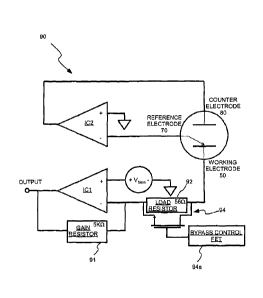
[53] Figure 1B illustrates schematically an embodiment of a portion or part
of
electronic or control circuitry 90 used in a number of studies of the sensors
hereof. Such
electronic circuitry is sometimes referred to as a potentiostatic circuit. In
a three-electrode
sensor as illustrated in Figure 1A, a predetermined potential difference or
voltage is
maintained between reference electrode 70 and sensing or working electrode 50
to control the
electrochemical reaction and to deliver an output signal proportional to the
current produced
by the sensor. As described above, working electrode 50 responds to the
analyte or target gas
by either oxidizing or reducing the gas. The redox reaction creates a current
flow that is
proportional to the gas concentration. Current is supplied to sensor 10
through counter
electrode 80. A redox reaction opposite to that of the reaction at the working
electrode takes
place at counter electrode 80, completing the circuit with working electrode
50. The potential
of counter electrode 80 is allowed to float. When gas is detected, the cell
current rises and
counter electrode 80 polarizes with respect to reference electrode 70. The
potential on counter
electrode 80 is not important, as long as the circuit provides sufficient
voltage and current to
maintain the correct potential of working electrode 50.
11
CA 03005273 2018-05-11
WO 2017/136407 PCT/US2017/015985
[541 The measuring
circuit for electrical circuitry 90 includes a single stage operational
amplifier or op amp IC I. The sensor current is reflected across a gain
resistor 91 (having a
resistance of 51a1 in the illustrated embodiment), generating an output
voltage. A load
resistor 92 (having a resistance of 56S1 in the illustrated embodiment) may be
chosen, for
example, via a balance between the fastest response time and best signal-to-
noise ratio.
1551 A control
operational amplifier 1C2 provides the potentiostatic control and
provides the current to counter electrode 80 to balance the current required
by working
electrode 50. The inverting input into IC2 is connected to the reference
electrode, but does
not draw any significant current from the reference electrode.
[56] During electronic interrogation of a sensor hereof such as sensor 10,
a non-faradaic
current is induced (for example, via application of energy to working
electrode 50). For
example, a step change in potential may be created which generates a non-
faradaic current.
The generated non-faradaic current can be used to monitor the sensor
functionality or health
as a result of the charging of the electrodes. However, as described above,
the sensor should
be returned to its normal bias potential or potential range for normal
operation in sensing a
target or analyte gas. The process of returning the sensor to its operating
bias or operating
potential difference (which may be zero) produces a current peak (a charge
build-up) in the
opposite direction. The current peak arising on return to the operating
potential difference
can take many of seconds to dissipate.
[57] The present inventors have discovered that information regarding
sensor health or
the state of the sensor may be obtained upon application of energy/electrode
potential
changes that are quite small and/or short in duration, and measuring/analyzing
single data
points or multiple data points over short time spans in a resultant
response/current curve.
Moreover, the present inventors have discovered that a rapid discharge of even
relatively
large current peaks arising when inducing a non-faradaic current in sensor 10
(or another
sensor hereof) and/or in returning sensor 10 (or another sensor hereof) to its
operating
potential difference may be achieved via active control of sensor electronics
90 (for example,
by decreasing a load resistance in electronic circuitry 90 between working
electrode 50 and
the point at which the output/response is measured after the test potential
difference has been
applied). In a number of embodiments, the load resistance between working
electrode 50 and
the output of operational amplifier ICI is decreased to a low value.
Subsequently, the load
resistance between working electrode 50 and the output of operational
amplifier ICI is
12
CA 03005273 2018-05-11
WO 2017/136407 PCT/US2017/015985
restored to its normal or operational load resistance (or to within an
operation range of load
resistance) after the charge is substantially dissipated or fully dissipated.
1581 In a number of
embodiments, load resistor 92 (see Figure 1B) is bypassed to
decrease the load resistance between working electrode 50 and the inverting
terminal of
operational amplifier ICI. A bypass circuit 94 may, for example, be provided
to bypass load
resistor 92. In a number of embodiments, a field effect transistor (FET) 94a
was used as a
switch in a bypass circuit 94 to controllably effect a bypass or short circuit
around load
resistor 92. In a number of embodiments, a metal-oxide-semiconductor FET or
MOSFET
was used.
[59] Figures 2A and 2B
illustrate the output of sensor 10 including a working
electrode 50 designed to detect hydrogen sulfide or H2S. In the studied
embodiment of
Figures 2A and 2B, working electrode 50 was formed by depositing an iridium
catalyst on a
diffusion membrane, reference electrode 70 was formed by depositing an iridium
catalyst on
a diffusion membrane, and counter electrode 80 was formed by depositing an
iridium catalyst
on a diffusion membrane. The bias potential or operating potential difference
of the sensor
was 0 mV. As illustrated in Figure 2A, at a time represented by point A, an
electronic
interrogation procedure is initiated. After 0.5 seconds (represented by point
B), a test
potential difference is applied. In the illustrated studies, a test potential
of +10 mV was
applied. A measured peak value (MPV) of output was recorded 1/16th of a second
after
application of the test potential as represented by point C. At that time, the
potential was also
returned to the operating potential difference of 0 mV. Figure 2A illustrates
the sensor output
when load resistor 92 is bypassed by activation of FET 94a and the sensor
output when load
resistor 92 is not bypassed. In the case where load resistor 92 is bypassed,
FET 94a was
activated at generally the same time or contemporaneously with return of the
potential to the
operating potential difference. As illustrated in Figure 2A, the significantly
lower load
resistance causes a significantly greater negative current spike (which would
be viewed as a
very high negative gas ppm reading in the normal mode of operation) than the
case in which
load resistor 92 is not bypassed. It was, therefore, surprising that the rapid
discharge which
occurs upon bypassing load resistor 92 returns the sensor output to the
baseline in a very
short period of time (that is, in less than 1 second). The contrast with the
case in which load
resistor 92 is not bypassed is best illustrated in Figure 2B in which the
output scale is
expanded. As illustrated in Figure 2B, the output returns to the baseline
output in less than
13
CA 03005273 2018-05-11
WO 2017/136407 PCT/US2017/015985
one second (that is, from t=0.5 seconds to t=z0.95 seconds) when load resistor
92 is bypassed,
whereas it takes many seconds for the output to return to the baseline output
when load
resistor 92 is not bypassed. As illustrated in Figure 2A, when FET 94a is
deactivated and
56 11 load resistor 92 is restored in the circuit at a time of approximately
0.95 seconds as
represented by point D, the output current is below a value that would be
discerned by the
end user. This value is typically in the range of approximately 0 to +2 ppm of
the target gas
[601 Figures 3A and 3B
illustrate the output of the H2S sensor when a test potential of
+10 mV is applied for I/64th of a second. Approximately 0.5 seconds after
initiation of the
test procedure at t-0, a test potential difference of +10 mV is applied. The
peak output value
was recorded 1/64th of a second after application of the test potential. At
that time, the
potential difference was also returned to the operating potential difference
of 0 mV.
Figure 3A illustrates both the sensor output when load resistor 92 is bypassed
by activation of
FET 94a, and the sensor output when load resistor 92 is not bypassed. In the
case where the
load resistor is bypassed, FET 94a was activated at generally the same time or
contemporaneously with return of the potential to the operating potential
difference. Once
again, the significantly lower load resistance causes a significantly greater
negative current
spike (that would viewed as a very high negative gas ppm reading in the normal
mode of
operation) than the case in which load resistor 92 is not bypassed. The
contrast with the case
in which load resistor 92 is not bypassed is best illustrated in Figure 3B in
which the output
scale is expanded. As illustrated in Figure 3B, similar to the results
illustrated in Figure 213,
although the output returns to the baseline output in less than one second
when load
resistor 92 is bypassed, it takes many seconds for the output to return to the
baseline output
when load resistor 92 is not bypassed (Figure 3B). The 56 SI load resistor 92
was restored in
the circuit at a time of less than 1 second from the initiation of the test
procedure.
1611 Figures 4A and 4B
illustrate the output of sensor 10 including a working
electrode 50 designed to detect carbon monoxide or CO in response to a +10 mV
test
potential difference lasting for 1/16th of a second. In the studied embodiment
of Figures 2A
and 213, working electrode 50 was formed by depositing an platinum catalyst on
a diffusion
membrane , reference electrode 70 was formed by depositing an platinum
catalyst on a
diffusion membrane, and counter electrode 80 was formed by depositing an
platinum catalyst
on a diffusion membrane. The bias potential or operating potential difference
of the sensor
was 180 mV. Similar to the studies described in connection with Figures 2A and
213,
14
CA 03005273 2018-05-11
WO 2017/136407 PCT/US2017/015985
approximately 0.5 seconds after initiation of the test procedure at a test
potential
difference of +10 mV is applied. The peak output value was recorded 1/16th of
a second after
application of the test potential and the potential difference was returned to
the operating
potential difference of 180 mV. Figure 4A illustrates sensor output when load
resistor 92 is
bypassed by activation of FET 94a and sensor output when load resistor 92 is
not bypassed.
In the case wherein load resistor 92 is bypassed, FET 94a was activated at
generally the same
time or contemporaneously with return of the potential to the operating
potential difference.
As with the H2S sensors studied in connection with Figures 2A through 3B, the
significantly
lower load resistance causes a significantly greater negative current spike
than is the case
when load resistor 92 is not bypassed. The contrast with the case in which
load resistor 92 is
not bypassed is best illustrated in Figure 4B in which the output scale is
expanded. As shown
in Figure 4B, although the output returns to approximately the baseline output
in less than
one second when load resistor 92 is bypassed, it takes many seconds for the
output to return
to the baseline output when load resistor 92 is not bypassed. The 56 C/ load
resistor 92 was
restored in the circuit, and the sensor returned to normal operation, at a
time of less than 1
second from the initiation of the test procedure. Figures 5A and 5B illustrate
similar results
with an application of a test potential difference of +10 mV for 1/64th of a
second.
[621 Figure 6 illustrates another embodiment of a sensor interrogation
methodology
hereof. In that regard Figure 6 illustrates the output of a sensor hereof in
response to a
+10 mV test potential difference lasting for approximately 1/16th of a second.
In this
embodiment, FET 94a is applied 3/64th of a second after the measured peak
value of output
(MPV), but prior to collection of a number of additional data points. At point
B, the potential
is increased from OmV to +10MV. The measured maximum peak value and a small
portion
of the positive decay curve are recorded. At point C, the FET is activated and
the potential is
returned to OmV. The current is then allowed to decay to near zero. This
methodology
allows more sensor data to be retrieved before FET 94a is activated while
reducing the
accumulated charge compared to techniques in which an increased potential is
applied for, for
example, 5-10 seconds. The smaller accumulated charge hereof translates into a
shorter
recovery time, but provides significant information regarding the state/health
of the sensor.
The measured peak value, the slope of the decay curve, the positive area under
curve (+AUC)
of the abbreviated decay curve, and the negative area under curve (-AUC) of
the current
discharge during FET activation are among the parameters that may collected.
More data
CA 03005273 2018-05-11
WO 2017/136407 PCT/US2017/015985
may be collected and potentially used for sensor interrogation while
shortening the recovery
time.
1631 Figure 7 illustrates
another embodiment of a methodology hereof in which an
applied potential is toggled between lower and higher values over two
interrogations cycles
(a "low" interrogation cycle and a "high" interrogation cycle). In the method
of Figure 7, a
positive potential step is applied at point B (for example, from 0 mV to +10
mV) during the
first of two interrogation cycles. Data collected may include the positive
measured peak
value as well as the nature of the abbreviated decay curve. FET 94a is
activated at point C.
However, the potential is not returned to the original potential at point C,
but is maintained at
the increased potential initiated at point B. Activating FET 94a quickly
discharges the curve
from the positive step initiated at point B. FET 94a is de-activated at point
D, before the
sensor/instrument resumes operation at the increased potential established at
point B (for
example, +10 mV). Thus, the sensor's operating potential is now at a higher
positive from its
original potential (0 mV for instance), even after the sensor has returned to
normal gas
detection operation. The sensor performs nominally as long as the original
potential is
chosen to be within a plateau region wherein small changes in potential do not
significantly
change sensor performance. At the initiation of the second interrogation at
point E, the
potential is toggled back to the original value (for example, 0 mV). The
resultant negative
response is characterized to draw data regarding sensor state/health. Once
again, data
collected may include the negative measured peak value as well as the nature
of the
abbreviated decay curve. FET 94a is activated at point F and data is collected
in the same
manner as described above. However, the current direction is opposite in
polarity.
1641 In addition to the
collected data described above, additional information may, for
example, be obtained by comparing the positive and negative responses (MPV+
vs. MPV-,
AUC+ vs. AUC-, slope of decay+ vs. slope of decay-). A similar toggling
approach may be
applied to the representative examples described in connection with Figures 2A
through 5B.
In the case of those representative embodiments, the FET may be activated
immediately after
the MPV is taken and the data available would include the MPV+ and the MPV-.
1651 Actions other than
decreasing resistance may be taken to rapidly discharge current
arising from, for example, a change in potential. Figure 8, for example,
illustrates a
representative example in which a series of potential step changes is applied
to discharge the
current. In this example, each consecutive potential step change is of a
smaller magnitude
16
CA 03005273 2018-05-11
WO 2017/136407 PCT/US2017/015985
and opposite polarity than the previous one. This process occurs until the
potential steps are
so small that the resulting current has returned to approximately zero. With
each consecutive
step change in potential, the current is driven in the opposite direction from
the previous step,
and the potential may, for example, be changed to the next potential when the
current is
measured to be approximately zero.
[66] In the
representative example of Figure 8, the potential is altered with very fast
pulses and only the MPV's are collected. Both the positive and negative MPV's
may be
collected. Sensor data may be collected and relationships analyzed. For
example, one may
analyze all of the MPV+ values and determine changes over time to predict
sensor health.
1671 In the example of
Figure 9, longer pulses of potential change than applied in the
representative example of Figure 8 are applied. MPV's and AUC's of abbreviated
decay
curves may be collected (as discussed in connection with Figure 7). Further,
the relationships
between these values over time may be used as sensor state/health predictors.
[68] Additionally, in
either of the representative examples of Figures 8 and 9, one may
calculate a magnitude and duration of the subsequent pulse from the
information obtained in
the previous pulse. In such an embodiment, instead of having a series of
potential steps with
predetermined magnitudes and durations, the system calculates, in real time,
an improved or
optimized sequence with the goal of more quickly dissipating the current. In
this approach,
the information from only the first potential step would typically be used as
a predictor of
sensor state/health as the first potential step would be the only one
guaranteed to be the same
between interrogation events. Once again, the subsequent pulses may be
optimized in real
time with the sole purpose of rapidly discharging the current. As such, the
subsequent
potential step pulses will be variable over time, potentially making it
difficult to predict
sensor performance from responses thereto.
1691 As described above,
instrument polling rates are currently designed to be
approximately 1 second. It is unlikely in the vast majority of situations that
future
instruments will be designed to sample faster that 1 second per data point.
Continued
advances in electronics (such as integrated circuit or ASIC design) allow for
further
optimizing sensor interrogation parameters. Such optimization allows faster
interrogation by,
for example, using pulses of smaller magnitudes and shorter durations than
described in the
above examples (see, for example, Figure 10). As the pulse amplitude/height
(that is,
17
CA 03005273 2018-05-11
potential step) gets smaller and the pulse duration gets shorter, the amount
of charge that is
produced during the interrogation is reduced and, consequently, the time
required to recover
is reduced. Active control of electronic circuitry of the sensor, such as via
reduction of
resistance (for example, using a FET), to dissipate charge may not be needed.
[70] Instead of applying a potential perturbation as a separate
interrogation event, a
potential waveform may be constantly applied across the sensor, and data
points may be
sampled at predetermined intervals within a cycle (see Figure 11). This
waveform may, for
example, be a step function. However, other waveforms may be used (for
example, a sine
wave, a triangle wave, etc.). This methodology is a variation of Figure 10. In
that regard, the
magnitudes and duration of the potential steps are of small enough magnitude
and short
enough duration to allow the current to discharge quickly. Data/Information
may be
collected at predetermined intervals during the potential waveform. For
example, MPV's,
AUC's and normal (analytical) gas readings may be taken at the same time
during each cycle.
[71] In a number of embodiments, described above, a short circuit was
created via a
FET to quickly dissipate charge. In a number of embodiments, one may, at the
same time as
activation of a FET or separately from activation of a FET/switch, apply a
pulse in the
opposite direction of a determined magnitude to pull off the original charge
that was applied
minus any loss of charge. The amount of charge can be readily determined by a
person
skilled in the electrical arts given the proper context. This result may also
be accomplished
with a current pulse rather than a voltage pulse.
[72] In a number of embodiments hereof, current is measured during a pulse
and
compared to a previously determined, calibrated value as described above. The
calibrated
value is determined during the last gas calibration (that is, at the time of
manufacture and at
subsequent gas calibrations of an instrument). Comparison of the calibrated
value and the
measured value not only provides a measurement of the state of the sensor, but
also provides
a means to adjust sensor output (for example, to correct for the sensor
sensitivity). In a
number of representative embodiments of systems, devices and/or methods hereof
an
internal, electronic check or interrogation of sensor functionality,
connection, may be made
as described herein (without the application of an analyte gas or a simulant
therefor) and
sensor output may be corrected as, for example, described in US Patent No.
7,413,645, the
disclosure of which may be referred to. A correction factor applied to sensor
output may, for
example, have the mathematical form:
18
CA 03005273 2018-05-11
WO 2017/136407 PCT/US2017/015985
Se= 1+ ' __ )a)S,
R0))
[731 In the above
equitation, Sc is the corrected sensitivity of the sensor, Ro and So were
the initial values of response function and sensitivity, respectively, Ri and
Si were the
response function and sensitivity, respectively, at any point in time during
the experiment,
and a was an adjustable parameter. The form of this equation is not unique;
other correction
functions may be used as well. The application of this correction factor to
the experimental
data brought the indicated response of the instrument back into the specified
range over the
entire course of the experiment, thereby eliminating the need to recalibrate
the sensor against
a known standard calibration gas.
[741 The foregoing
description and accompanying drawings set forth a number of
representative embodiments at the present time. Various modifications,
additions and
alternative designs will, of course, become apparent to those skilled in the
art in light of the
foregoing teachings without departing from the scope hereof, which is
indicated by the
following claims rather than by the foregoing description. All changes and
variations that fall
within the meaning and range of equivalency of the claims are to be embraced
within their
scope.
19