Note: Descriptions are shown in the official language in which they were submitted.
INTERNAL PARALLELED ACTIVE NEUTRAL POINT CLAMPED CONVERTER
WITH LOGIC-BASED FLYING CAPACITOR VOLTAGE BALANCING
FIELD OF THE INVENTION
[00011 The present invention relates to an internal parallelization based
active neutral
point clamped (IP-ANPC) converter, and more particularly to a modular internal
parallelization based active neutral point clamped (IP-ANPC) converter with
logic-based
flying capacitor voltage balancing.
BACKGROUND OF THE INVENTION
[0002] Multilevel converters have been widely applied in applications
like high
voltage DC transmission (HVDC), medium voltage (MV) and low voltage (LV)
drives,
and PV inverters. The foremost advantages of multilevel converters include
reduced device
voltage stress, improved output quality, better common mode voltage profile,
system
efficiency improvement, etc. With the penetration of wide band-gap (WBG)
devices, i.e.
Silicon Carbide (SiC) and Gallium Nitride (GaN), multilevel becomes even more
favorable
due to the following reasons. First of all, the WBG devices have limited
voltage rating and
series connection of WBG devices are challenging. Secondly, the dv/dt issue of
WBG
device poses challenges for overvoltage mitigation and noise suppression. With
a
multilevel converter, these challenges can be alleviated to a great extent.
Conventionally,
three-level (3L) converters, e.g. neutral point clamped (NPC) converter and T
type NPC
(TNPC), are popular choices. But to further improve the system performances,
topologies
with higher number of voltage levels are attractive. In general, increasing
the number of
1
CA 3005583 2018-05-22
voltage levels can improve the output quality and mitigate common mode voltage
(CMV)
as well as leakage current issues. Therefore, in recent years, intensive
studies on high-level
topologies, e.g. five-level (5L) and seven-level (7L), are reported in the
literature [1].
100031 Modularity has been favorable for reliability and economic
considerations.
Cascaded H-bridge (CHB) converter [2] and modular multilevel converter (MMC)
[3] are
good candidates in this category. However, both are more favorable for medium
and high
voltage applications. The bulky transformer and the unidirectional power flow
make the
CHB converter less attractive. As for the MMC, sub-module capacitor voltage
balancing
has been an issue for motor drive applications. Besides CHB and MMC, full DC
link
topologies like the flying capacitor based active neutral point clamped (FC-
ANPC)
converters [4] have been proposed. However, these topologies are not modular
in design.
[0004] In addition, paralleling several converters to achieve higher
power capacity is
a popular solution for many applications [5-7]. First of all, parallelization
offers modularity
and fault tolerant capability. Secondly, the current rating of WBG devices
will be much
lower than that of the Silicon (Si) devices for a long time to come, and thus
to reach higher
power rating, parallelization becomes the only feasible solution. Thirdly,
interleaving
operation of the paralleled converters provides opportunities for output
quality
improvement, DC link current stress reduction, and CMV reduction [6-8]. With
the
adoption of WBG devices and higher switching frequency, circulating current
can be
reduced, providing great opportunity for interleaving operation. Lastly, our
recent study
found that interleaving of higher-level converters produces lower circulating
current [9].
However, parallelization of high-level converters is seldom considered due to
the concerns
2
CA 3005583 2018-05-22
of undermined reliability due to high device count, and increased cost due to
higher cost
of WBG devices. In particular, a high-level converter fully built with WBG
devices will
be very costly, and thus paralleling of full-WBG converters becomes even less
attractive.
100051 Thus, there exists a need for a modularized and cost effective
high-level
multilevel converter topology concept that enables better utilization of WBG
devices in
high power applications. At the same time, as the switching frequency can be
very high,
an implicit but important requirement for WBG device-based topologies is that
the
modulation and control of the topology should be simple.
SUMMARY OF THE INVENTION
[0006] The present disclosure provides an internal parallelization based
active neutral
point clamped (IP-ANPC) converter that includes a low switching frequency
(LSF) part
and a plurality of high switching frequency (HSF) modules. The HSF modules are
connected in parallel. According to embodiments, the converter includes an
output filter.
The converter is modular.
[0007] According to various embodiments the HSF modules each include a
current
sharing inductor. In some embodiments, each HSF module has a flying capacitor.
The HSF
modules may be synchronized. In further embodiments, each HSF module of the
plurality
of HSF modules is a half bridge HSF module. In embodiments, the HSF modules
are
interleaved.
3
CA 3005583 2018-05-22
[0008] According to embodiments of the present disclosure, voltage of the
converter
is balanced naturally with phase shift pulse width modulation. In various
embodiments,
voltage of the converter is redundantly balanced with redundant switching
states.
BRIEF DESCRIPTION OF THE DRAWINGS
[0009] The subject matter that is regarded as the invention is
particularly pointed out
and distinctly claimed in the claims at the conclusion of the specification.
The foregoing and
other objects, features, and advantages of the invention are apparent from the
following
detailed description taken in conjunction with the accompanying drawings in
which:
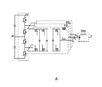
[0010] FIG. 1A is a schematic drawing showing one phase leg of a
generalized IP-
ANPC converter;
[0011] FIG. 1B is a schematic drawing showing an IP-ANPC with a single
neutral point
DC link type using single flying capacitor module, FC-IP-ANPC;
[0012] FIG. 1C is a schematic drawing showing an IP-ANPC with a single
neutral point
DC link type using a half-bridge module, HB-IP-ANPC;
[0013] FIG. 1D is a schematic drawing showing an IP-ANPC converter based
on 5L
ANPC;
[0014] FIG. 2A is a schematic drawing showing IP-ANPC topology using HSF
module
with only one flying capacitor;
[0015] FIG. 2B is a schematic drawing showing IP-ANPC topology using HSF
module
with multiple flying capacitors;
4
CA 3005583 2018-05-22
[0016] FIG. 2C is a schematic drawing showing IP-ANPC topology using half
bridge
modules;
[0017] FIG. 3. Is a graph showing normalized MTBF value with different
number of
paralleled HSF modules;
[0018] FIG. 4 is a graph showing normalized MTBF value with additional
installed HSF
module with the value N indicating that the actual installed number of HSF
modules is N+1;
[0019] FIG. 5 is a graph showing simulated conduction loss of LSF devices
per phase;
[0020] FIG.6A is a series of graphs showing phase voltage (Van), line-to-
line voltage
(V11), and common mode voltage (CMV) waveforms of the embodiment of FIG. 1B
with
two HSF modules in an SO operation mode for HB-IP-ANPC;
[0021] FIG.6B is a series of graphs showing phase voltage (Van), line-to-
line voltage
(V11), and common mode voltage (CMV) waveforms of the embodiment of FIG. 1B
with
two HSF modules in an 10 operation mode for HB-IP-ANPC and SO mode for FC-IP-
ANPC;
[0022] FIG.6C is a series of graphs showing phase voltage (Van), line-to-
line voltage
(V11), and common mode voltage (CMV) waveforms of the embodiment of FIG. 1B
with
two HSF modules in an 10 operation mode for FC-IP-ANPC;
[0023] FIG. 7A is a series of graphs showing Harmonic spectral of the
waveforms in an
SO operation mode for HB-IP-ANPC;
[0024] FIG. 7B is a series of graphs showing Harmonic spectral of the
waveforms in an
operation mode for HB-IP-ANPC and an SO operation mode for FC-IP-ANPC;
5
CA 3005583 2018-05-22
[0025] FIG. 7C is a series of graphs showing Harmonic spectral of the
waveforms in an
operation mode for FC-IP-ANPC;
[0026] FIG. 8A is a graph showing PWM strategies of an SO mode of FC-IP-
ANPC;
[0027] FIG. 8B is a graph showing PWM strategies of an JO mode of FC-IP-
ANPC;
[0028] FIG. 8C is a graph showing PWM strategies of an SO mode of HB-1P-
ANPC;
[0029] FIG. 8D is a graph showing PWM strategies of an 10 mode of HB-IP-
ANPC;
[0030] FIG. 9A shows an inductor implementation schemes in one phase with
two HSF
modules and two separated DM inductors;
[0031] FIG. 9B shows an inductor implementation schemes in one phase with
two HSF
modules and one coupled inductor and one DM inductor;
[0032] FIG. 10 is a schematic drawing showing an implementation principle
of a logic
based flying capacitor voltage balancing scheme according to the present
disclosure;
[0033] FIG. 11A is a graph showing total output voltage and output
current of FC-IP-
ANPC in an 10 operation mode;
[0034] FIG. 11B is a graph showing output voltage of each HSF module and
the total
output voltage of FC-IP-ANPC in an 10 operation mode;
[0035] FIG. 11C is a graph showing harmonic spectrum of the total output
voltage of
FC-IP-ANPC in an 10 operation mode;
[0036] FIG. 12A is a graph showing total output voltage and output
current of HB-IP-
ANPC in an 10 operation mode;
[0037] FIG. 12B is a graph showing output voltage of each HSF module and
the total
output voltage of HB-IP-ANPC in an 10 operation mode; and
6
CA 3005583 2018-05-22
[0038] FIG. 12C is a graph showing harmonic spectrum of the total output
voltage of
HB-IP-ANPC in an 10 operation mode.
DESCRIPTION OF THE PREFERRED EMBODIMENTS
[0039] The present invention has utility as an internal parallelization
based active
neutral point clamped (IP-ANPC) converter that provides benefits of
modularity, improved
reliability and efficiency, interleaving operation, and reasonable utilization
of WBG
devices.
[0040] Many objects of this invention will appear from the following
description and
appended claims, reference being made to the accompanying drawings forming a
part of
this specification wherein like reference characters designate corresponding
parts in the
several views.
[0041] Before explaining at least one embodiment of the invention in
detail, it is to be
understood that the invention is not limited in its application to the details
of construction
and the arrangements of the components set forth in the following description
or illustrated
in the drawings. The invention is capable of other embodiments and of being
practiced and
carried out in various ways. It is important, therefore, that the claims be
regarded as
including such equivalent constructions insofar as they do not depart from the
spirit and
scope of the present invention. Also, it is to be understood that the
phraseology and
terminology employed herein are for the purpose of description and should not
be regarded
as limiting.
7
CA 3005583 2018-05-22
[0042] It is to be understood that in instances where a range of values
are provided
that the range is intended to encompass not only the end point values of the
range but also
intermediate values of the range as explicitly being included within the range
and varying
by the last significant figure of the range. By way of example, a recited
range of from 1 to
4 is intended to include 1-2, 1-3, 2-4, 3-4, and 1-4.
[0043] The present disclosure provides internal parallelization based
active neutral
point clamped (IP-ANPC) topologies and IP-ANPC converters as shown generally
in
FIGS. 1A-1D. The architecture takes advantages of an interesting feature of
the
conventional FC-ANPC topology, i.e. the topological decoupling of a
fundamental
switching frequency (FSF) part and a high switching frequency (HSF) part.
Therefore,
several HSF modules can be paralleled and connected to the same FSF base
module. By
doing so, parallelization is realized without significantly increasing the
device count,
whereas the merits of parallelization, i.e. modularity and possible
interleaving operation,
are still retained.
[0044] The proposed topology provides an alternative solution for
applications where
parallelization is usually used, e.g. wind turbine generator and large scale
PV plant. For
applications like industry and traction drives where single converter is more
applied, the
proposed topology can also be implemented due to the improvements in
efficiency and
reliability. Furthermore, with the IP-ANPC converter, WBG devices can be
readily
implemented in many high power applications with better device utilization.
Finally, the
interleaving operation of the paralleled HSF modules provides additional
opportunity for
realizing higher-level output voltage. In recent years, seeking high-level
topologies based
8
CA 3005583 2018-05-22
on 5L ANPC converter is becoming popular [10-12]. However, none of the
previous
topologies are modular in design.
[0045] As shown
in FIGS. 1A-1D, each topology includes a low switching frequency
(LSF) part and several (N, N>=2) parallel-connected high switching frequency
(HSF)
modules. To prevent short circuit, each HSF module includes a current sharing
inductor,
which can also serve as (at least part of) an output filter. In the embodiment
shown in FIG.
1B, each HSF module has one flying capacitor. The output voltage with this
embodiment
is 5-level if the HSF modules are synchronized and will be higher-level if the
HSF modules
are interleaved, e.g. 9-level when N = 2, and 13-level when N = 3. The
embodiment shown
in FIG. 1C utilizes half-bridge based HSF modules. If HSF modules are
synchronized, the
output is 3-level, but if interleaved, higher-level output can be generated,
e.g. 5-level when
N = 2, and 7-level when N = 3. The embodiments of the present disclosure
realize higher-
level output with only one neutral point (NP) in the DC link, and at the same
time without
using cascaded H-bridges [10] at the output. With only one DC link NP, the NP
voltage
can be self-balanced along the entire modulation index and power factor range.
It also can
be easily controlled. Moreover, without using cascaded H-bridges, the flying
capacitor
voltage (for the embodiment in FIG. 1B) can be self-balanced. Again, it also
can be actively
balanced for protection purpose. A fast and simple active balancing method is
also
provided by the present disclosure. The above advantages can significantly
increase the
operation reliability and reduce the control complexity of the system, making
them
attractive for WBG devices. Another advantage of the IP-ANPC topologies is
that the
system reliability of can be improved as compared to conventional converter
9
CA 3005583 2018-05-22
parallelization. With a backup HSF module, the system reliability can be
extremely high,
which is attractive for critical applications. FIG. 1D shows five-level ANPC
(5L ANPC)
topology based architecture (5L IP-ANPC) with two HSF modules.
[0046] According to embodiments of the present disclosure, the HSF modules in
the IP-ANPC converter are identically designed, making the topology
modularized. This
inherent modularity facilitates the design of the system and meanwhile enables
the fault
tolerant capability. In addition, the HSF modules are designed with partial
power, which
allows a device with lower current rating, and thus lower cost, to be used and
alleviating
the pressure of manufacture, maintenance, and repair.
[0047] As for
reliability, the reliability of a system has an inverse relationship with the
number of installed device. Typically, parallelization undermines the
reliability of the
system. This is particularly important for multilevel converters as they
usually have higher
device count. This problem is alleviated with the IP-ANPC architecture. FIG. 3
shows the
Mean Time Between Failures (MTBF) value (normalized to single 5L ANPC
converter)
with respect to the ratio of the failure rate between HSF module and LSF
module
(Xi isFaisF). The MTBF is calculated based on Equation 1. In FIG. 3, the
dashed lines show
the reliability of paralleled 5L ANPC converters, with the color indicating
the number of
converters. As one can see, the IP-ANPC is more reliable than the paralleled
converters.
Note that with practical considerations, the ratio between the failure rates
of HSF module
and LSF module is usually within 5 [12], which indicates that the improvement
brought by
IP-ANPC topology is significant.
CA 3005583 2018-05-22
1
¨
Equation 1: MTBF IP 11
hs'TsF N (1
[0048] In
addition, with each additionally installed HSF module, i.e. N+1 strategy, the
reliability can be boosted as compared to non-modular designs. The normalized
MTBF
with additional HSF modules, calculated based on Equation 2, is shown in FIG.
4. Note
that the repair rate j.t of the HSF module is considered in the calculation.
It is clear to see
that with additional installed HSF modules, the reliability of the system can
be much higher
than that of the single converter system. The variable kin FIG. 4 denotes the
ratio between
P=IISF and XHSF. With more HSF modules in parallel, there is an opportunity to
increase the
value of k as repairing is easier with modular design.
1
MTBFIP,N+1 = ___________
Equation 2: N(N +1)14,2
I ISF
1 a 4
Fsi,
(2N + 1) A1ISF
[0049]
Parallelization is an effective way to reduce the total switching loss of the
system [11]. However, it is difficult to reduce conduction loss. For an IGBT
device with
anti-parallel diode, the conduction loss can be calculated based on Equation 3
for the
switching and based on Equation 4 for the diode. Two IGBT modules with
different current
ratings but the same technology will have very similar VcEo and VFo. However,
the on-state
resistance (Rc and RF) is in general inversely proportional to the current
rating. Therefore,
for the same total current, the total conduction loss of two low current
rating devices will
be very close to that of one high current rating device. That said,
parallelization generally
does not reduce the total conduction loss of the system.
11
CA 3005583 2018-05-22
P
Equation 3: Con, IGBT = vCEO/C, Avg + RciC2,RMS
2
Equation 4: P Con,Diode = VFO/D, Avg + R FI D,RMS
[0050] For an IP-ANPC converter according to the present disclosure, the
LSF devices
are dominated by conduction loss as their switching losses are negligible.
However, the
HSF devices are dominated by switching losses due to the required high
switching
frequency. Therefore, parallelization of LSF module is actually unnecessary as
it provides
no further efficiency improvement. However, the parallelization of HSF modules
can be a
benefit.
[0051] The IP-ANPC topology is particularly attractive for WBG devices.
Due to the
limited voltage (-1.7kV) and current rating (-300A), the WBG devices are not
readily
applied for many high power applications with conventional solutions, e.g. the
traction
drives in high-speed rail (HSR), megawatt scale 1.5kV large scale PV inverter,
and multi-
megawatt wind turbine. These applications require not only high blocking
voltage, but also
high current rating, both of which are limited in WBG devices. Hence, Si IGBT
based 2L
converters will be still prevailing in industry. However, with the inventive
IP-ANPC
topology, the Si IGBT can be used to construct the LSF modules, while WBG
devices can
be implemented in HSF modules. As such, the voltage stress on the WBG devices
is
reduced as compared to 3L topologies. The parallelization of HSF modules can
reduce the
current stress and total switching losses of the WBG devices. Also, the high
switching
capability of WBG in turn reduces the size of flying capacitor and current
sharing
12
CA 3005583 2018-05-22
inductors. As high switching frequency and high-level output can significantly
reduce the
size of input/output filters, the power density and power weight (Power/Mass)
of the entire
system can be substantially increased.
100521
According to embodiments of the present disclosure, Si IGBT is used as the
LSF devices. Si IGBT has much higher voltage and current rating than the state-
of-the-art
WBG devices. Therefore, for many applications, there are no WBG devices
available for
LSF module design. Secondly, the benefit of switching loss reduction with WBG
device
cannot be reflected in LSF module. Nevertheless, the conduction loss of Si
IGBT and WBG
devices are actually very similar. Table I shows two selected devices for
comparison of
conduction loss. Both are 1.2kV and 300A rated. A simulation is conducted
based on a 240
kVA three-phase FC-IP-ANPC converter with 1,2kV DC link voltage and 690V AC
output. Constant impedance load is used such that the output current is
proportional to the
modulation index. The simulated conduction loss per phase is shown in FIG. 5.
The
maximum difference only accounts for a negligible 0.06% difference in the
efficiency of
the system. In heavy a load condition, the conduction loss with Si IGBT is
even lower.
Therefore, it is reasonable to implement Si IGBT as LSF devices. The cost of
the system
can also be reduced as Si IGBT has much lower cost than WBG devices. Also, as
the
current rating of Si IGBT is much higher than that of WBG devices, using IP-
ANPC
topology becomes a favorable solution as paralleling of several LSF module is
quite
unnecessary. In addition, the number of installed WBG devices in the IP-ANPC
topology
is the same or less as compared to the state-of-the-art full WBG 3L
converters.
Table I. Device parameters at junction temperature of 150 C.
13
CA 3005583 2018-05-22
Model Type VCEO Rc /
Rds,on
FF300R12KT4P Si 0.7V 4.3m1
CAS300M12BM2 SiC N/A 7.7mn
100531 Interleaving is an effective way to increase the number of output
voltage levels.
Such interleaving can be series type, i.e. flying capacitor converter or
parallel type, i.e.
interleaved converter through current sharing inductors [13]. With series
type, many
capacitors are required, whereas higher volume of inductors are required in
parallel
interleaving in order to suppress the circulating current. Hybrid series-
parallel interleaving
with interleaved flying capacitor converters is a good alternative, as
interleaved multilevel
converters tend to have lower circulating current as compared to interleaved
2L converters
[9]. But as aforementioned, high device count leads to reliability
degradation. The proposed
IP-ANPC topology provides a new solution for hybrid series-parallel
interleaving with
lower device count, and thus higher reliability. In the following context,
simulation results
are presented using the system specs in Table II.
Table II. System specifications
Parameter Value
DC link voltage 1200V
Carrier frequency 3000Hz
Current sharing inductance 50uH for SO mode; 2.5mH for JO mode
Flying capacitor capacitance 100uF
14
CA 3005583 2018-05-22
No. of HSF modules 2
Load parameters 690V/5 OkW
100541 As with interleaved converters, the number of output voltage
levels can be
increased with interleaving of the HSF modules. For example, for the FC-IP-
ANPC, 9L
output can be obtained if two HSF modules are interleaved, and 13L output for
interleaved
HSF modules. As such, the output quality can be improved. At the same time,
the CMV
issue is also mitigated. FIGS. 613 and 6C show the example waveforms of phase
voltage
and CMV with phase-shifted PWM (see FIGS. 8A and 8B) in synchronized operation
(SO)
and interleaved operation (JO) modes, respectively, with two HSF modules. One
can see
that the resultant 9L CMV waveform is more desired than the 5L one.
Corresponding
harmonics spectral are presented in FIGS. 7B and 7C. The output voltage and
CMV both
contain less harmonics as compared to the non-interleaving case. The example
waveforms
of the HB-IP-ANPC are also presented, with FIG. 6A showing the results of SO
mode and
FIG. 6B showing the 10 mode. The harmonic spectral of the two modes are shown
in FIGS.
7A and 7B, respectively. One can see that after interleaving, the output
becomes 5L and
CMV is reduced. Note that the TO mode example waveforms for the HB-IP-ANPC are
obtained with the modulation strategy shown in FIG. 8D. Therefore, the results
are the
same as the 5L case with the modulation strategy shown in FIG. 8A. Similar to
the
interleaved 2L converters, separated differential mode (DM) inductors or
coupled-
inductors can be used to suppress the circulating current. The inductor
implementation
schemes are shown in FIG. 9.
CA 3005583 2018-05-22
[0055] The flying capacitor voltage, vFc, of the FC-IP-ANPC converter can
be
balanced at high frequency, naturally with phase-shift PWM or actively using
the
redundant switching states. Natural balancing is simple for implementation.
However,
according to some embodiments, a backup active balancing method is used for
protection
purposes when vFc becomes unstable or beyond set limits. There have been
several active
balancing approaches proposed in literature, e.g. the PI controller based
method [14], space
vector modulation (SVM) based [15], and cost function based [16]. For high
power
applications, these approaches can achieve good performance, even though they
are usually
complicated or time-consuming. However, for FC-IP-ANPC converter, a carrier-
based
balancing strategy is preferred in order to simplify the coordination of the
paralleled HSF
modules. Particularly, when WBG devices are implemented, existing methods will
significantly increase the computational burden of the control, and thus are
less practical.
As such, an efficient flying capacitor balancing becomes highly desirable.
[0056] To address the above challenge, the present disclosure provides a
logic based
flying capacitor voltage balancing scheme. The logic based method is very
flexible as it
can be adaptive to all kinds of PWM strategies, e.g. carrier-based, SVM,
selective harmonic
elimination PWM (SHE PWM), or any specially design strategy for a certain
purpose [17].
Its implementation in FC-IP-ANPC converter is also discussed.
[0057] The logic modulation scheme of the present disclosure is shown in
FIG. 10,
where S5R and S6R are the reference pulses when flying capacitor voltage
balancing is not
considered. These reference pulses can be generated through various 5L PWM
strategies,
as aforementioned. The flying capacitor voltage and output current are
measured, based on
16
CA 3005583 2018-05-22
which the controller then finds out the proper pulses for switches S5 and S6
(FIG. 1B) to
make sure the flying capacitor voltage is restrained around the reference
value. In the logic
based modulation, a variable A is defined as: if output current io >0, A = 1;
otherwise A =
0. Variable B is defined as, when the flying capacitor voltage vFc > vREF, B =
1, otherwise
B = 0. Variable D is defined as written in Equation 5. Also, to determine
whether or not
vFc should be balanced, another variable C and an Exclusive Or operation can
be
introduced into the calculation. When the pulses for S5R and S6R are
different, C = 1, which
means that vFc balancing should be carried out. Otherwise if C = 0, vFc
balancing is not
necessary. Based on this principle, the variable C can be obtained by Equation
6. After
having the value of D and C, the logic equations in Equation 7 are then used
to generate
the PWM signals for S5 and S6. Table III shows the logic table when active
balancing is
required, i.e. C = 1.
D = X0R(A, B)
Equation 5:
Equation 6: C = X0R(S5R S6R )
S5= S5R&C + D& C
Equation 7: S6 = S6R & & C
Table III. Logic table of the flying capacitor voltage balancing.
A B S5 S6
1 1 1 0 1
1 1 0 1 0
17
CA 3005583 2018-05-22
1 0 1 1 0
1 0 0 0 1
[0058] According to embodiments of the FC-IP-ANPC converter, the flying
capacitor
voltage of each HSF module in the same phase should have the same ripple
waveform.
However, this is usually not the case in practical applications. Particularly,
for interleaved
operation, the reference pulses of difference HSF modules are different.
Therefore, it is
necessary to measure the voltage on each flying capacitor and balance them
individually.
Experimental Results
[0059] Experimental results are obtained with a low voltage proof-of-
concept single
phase-leg prototype. The LSF part is built with discrete Si IGBT and switches
at 60Hz.
The HSF modules are built with GaN HEMT and switch at 301(Hz. The DC link
voltage is
80V. The flying capacitor is built with film capacitor with 50uF. The current
sharing
inductor is 2.5mH and the load is 6.5f/. The modulation index is 0.9. The
waveforms and
corresponding spectral of FC-IP-ANPC are shown in FIGS. 11A-11C with TO mode
only.
The waveforms and harmonic spectral of HB-IP-ANPC are shown in FIGA. 12A-12C
with
TO mode only. In the figures, Vtt stands for the total output voltage
(20V/div), Itt means the
total output current (2.5A/div), VHSF1 and VHSF2 are the output voltage of
HSF1 module
and HSF2 module, respectively (50V/div).
[0060] As shown in FIGS. 11A-11C, the output voltage of each HSF module
is 5L,
whereas the total output voltage becomes 9L due to interleaving. As shown in
FIG. 11C,
18
CA 3005583 2018-05-22
the lowest high frequency harmonics are around 120kHz, which is four times of
the
switching frequency, i.e. 30kHz. For the results of HB-IP-ANPC, one can see
that the
output voltage is 5L after interleaving, whereas the output voltage of each
HSF module is
3L. The effective switching frequency is 60kHz due to interleaving. The total
output
voltage THD values are 19.52% and 36.65% for FC-IP-ANPC and HB-IP-ANPC,
respectively.
[0061] The attached appendix, Appendix A (totaling 6 pages), references
cited therein,
and all references cited herein are hereby incorporated by reference in their
entireties
[0062] While at least one exemplary embodiment has been presented in the
foregoing
detailed description, it should be appreciated that a vast number of
variations exist. It
should also be appreciated that the exemplary embodiment or exemplary
embodiments are
only examples, and are not intended to limit the scope, applicability, or
configuration of
the described embodiments in any way. Rather, the foregoing detailed
description will
provide those skilled in the art with a convenient roadmap for implementing
the exemplary
embodiment or exemplary embodiments. It should be understood that various
changes may
be made in the function and arrangement of elements without departing from the
scope as
set forth in the appended claims and the legal equivalents thereof.
19
CA 3005583 2018-05-22
CITED REFERENCES
[1] S. Kouro et al., "Recent Advances and Industrial Applications of
Multilevel
Converters," IEEE Trans. Ind. Electron., vol. 57, no. 8, pp. 2553-2580, Aug.
2010.
[2] J. Rodriguez, S. Bernet, B. Wu, J. 0. Pontt and S. Kouro, "Multilevel
Voltage-Source-
Converter Topologies for Industrial Medium-Voltage Drives," IEEE Trans. Ind.
Electron., vol. 54, no. 6, pp. 2930-2945, Dec. 2007.
[3] M. A. Perez, S. Bernet, J. Rodriguez, S. Kouro and R. Lizana, "Circuit
Topologies,
Modeling, Control Schemes, and Applications of Modular Multilevel Converters,"
IEEE Trans. Power Electron., vol. 30, no. 1, pp. 4-17, Jan. 2015.
[4] P. Barbosa, P. Steimer, J. Steinke, M. Winkelnkemper and N. Celanovic,
"Active-
neutral-point-clamped (ANPC) multilevel converter technology," 2005 European
Conference on Power Electronics and Applications, Dresden, 2005, pp. 10 pp.-
P.10.
[5] F. Ueda, K. Matsui, M. Asao, K. Tsuboi, "Parallel-connections of
pulsewidth
modulated inverters using current sharing reactors", IEEE Trans. Power
Electron., vol.
10, no. 6, pp. 673-679, Nov. 1995.
[6] Z. Quan; Y. Li, "Suppressing Zero-Sequence Circulating Current of Modular
Interleaved Three-Phase Converters Using Carrier Phase Shift PWM," IEEE Trans.
Ind. Appl., in press, 2017.
[7] Z. Quan, Y. W. Li, "A Three-Level Space Vector Modulation Scheme for
Paralleled
Converters to Reduce Circulating Current and Common-Mode Voltage," IEEE Trans.
Power Electron., vol. 32, no. 1, pp. 703-714, Jan. 2017
[8] Z. Quan, Y. Li, "Impact of carrier phase shift PWM on the DC link current
of single
and interleaved three-phase voltage source converters", ECCE 2017.
[9] Z. Quan, Y. Li, "Harmonic Analysis of Interleaved Voltage Source
Converters and
Tr-Carrier PWM Strategies for Three-Level Converters", COMPEL 2017.
[JO] J. Li, S. Bhattacharya and A. Q. Huang, "A New Nine-Level Active NPC
(ANPC)
Converter for Grid Connection of Large Wind Turbines for Distributed
Generation,"
IEEE Trans. Power Electron., vol. 26, no. 3, pp. 961-972, March 2011.
[11] M. Kasper, D. Boras and J. W. Kolar, "Scaling and balancing of multi-cell
converters,"
2014 International Power Electronics Conference (IPEC-Hiroshima 2014 - ECCE
ASIA), Hiroshima, 2014, pp. 2079-2086.
[12] F. Richardeau and T. T. L. Pham, "Reliability Calculation of Multilevel
Converters:
Theory and Applications," IEEE Trans. Ind. Electron., vol. 60, no. 10, pp.
4225-4233,
Oct. 2013.
[13] J. W. Kolar, et al., Impact of Magnetics on Power Electronics Converter
Performance
- State-of-the-Art and Future Prospects, Keynote Presentation at the PSMA
Workshop
CA 3005583 2018-05-22
on "Power Magnetics @ High Frequency ¨ Transforming the Black Magic to
Engineering", Tampa, USA, March 25, 2017.
[14] M. Khazraei, H. Sepahvand, K. A. Corzine and M. Ferdowsi, "Active
Capacitor
Voltage Balancing in Single-Phase Flying-Capacitor Multilevel Power
Converters,"
IEEE Trans. Ind. Electron., vol. 59, no. 2, pp. 769-778, Feb. 2012.
[15] S. Choi and M. Saeedifard, "Capacitor Voltage Balancing of Flying
Capacitor
Multilevel Converters by Space Vector PWM," IEEE Trans. Power Del., vol. 27,
no.
3, pp. 1154-1161, July 2012.
[16] A. M. Y. M. Ghias, J. Pou and V. G. Agelidis, "Voltage-Balancing Method
for Stacked
Multicell Converters Using Phase-Disposition PWM," IEEE Trans. Ind. Electron.,
vol.
62, no. 7, pp. 4001-4010, July 2015.
[17] A. K. Sadigh, V. Dargahi and K. A. Corzine, "New Active Capacitor Voltage
Balancing
Method for Flying Capacitor Multicell Converter Based on Logic-Form-
Equations,"
IEEE Trans. Ind. Electron., vol. 64, no. 5, pp. 3467-3478, May 2017.
[18] J. Li, S. Bhattacharya and A. Q. Huang, "A New Nine-Level Active NPC
(ANPC)
Converter for Grid Connection of Large Wind Turbines for Distributed
Generation,"
IEEE Trans. Power Electron., vol. 26, no. 3, pp. 961-972, March 2011.
[19] P. Barbosa, P. Steimer, J. Steinke, M. Winkelnkemper and N. Celanovic,
"Active-
neutral-point-clamped (ANPC) multilevel converter technology," 2005 European
Conference on Power Electronics and Applications, Dresden, 2005, pp. 10 pp.-
P.10.
[n] H. Yu, B. Chen W. Yao and Z. Lu "Hybrid Seven-Level Converter Based on T-
Type
Converter and El-Bridge Cascaded Under SPWM and SVM "in IEEE Transactions on
Power Electronics, vor. 33, no. 1, pp. 689-702, Jan. 2018.
[21] S. R. Pulikanti, G. Konstantinou and V. G. Agelidis, "Hybrid Seven-Level
Cascaded
Active Neutral-Point-Clamped-Based Multilevel Converter Under SHE-PWM," in
IEEE Transactions on Industrial Electronics, vol. 60, no. 11, pp. 4794-4804,
Nov. 2013
21
CA 3005583 2018-05-22