Note: Descriptions are shown in the official language in which they were submitted.
DESCRIPTION
SILICON OPTICAL CIRCUIT FOR DETECTING FLAWS IN AN OPTICAL CIRCUIT
ELEMENT BASED ON LIGHT TRANSMITTANCE CHARACTERISTICS
Technical Field
[0001] The present invention relates to a silicon optical
circuit formed with a silicon optical waveguide, and, more
particularly, to the silicon optical circuit for detecting a flaw
occurred on the waveguide at a wafer state.
Background Art
[0002] Recently, vigorous research and development of a silicon
photonics technique capable of drastically downsizing optical
circuits are underway by applying a manufacturing technique of
silicon integrated electronic circuits to the formation of optical
waveguides and the like. Circuits having various functions are
proposed as silicon optical circuits based on the silicon photonics
technique, and development for their practical use is particularly
conducted in the field of an optical transceiver.
[0003] Fig. 27A and Fig. 27B are diagrams each showing a typical
configuration of an optical modulation circuit as a first example
of a silicon optical circuit of a conventional technique. Each of
optical circuits 9100-1 and 9100-2 in Fig. 27A and Fig. 27B is an
optical modulation circuit chip of a digital coherent polarization
multiplexed system which is applied to an optical transceiver mainly
for long distance transmission. Both of the optical circuits include
the same elements, which include an input waveguide 9101, optical
splitters 9102 to 9108, optical phase modulation waveguides 9109 to
- 1 ¨
Date Recue/Date Received 2020-04-17
CA 03005704 2018-05-17
9112 configuring four Mach-Zehnder circuits, optical couplers 9113
to 9118, a polarization rotation circuit 9119, a polarization
combining circuit 9120, and an output waveguide 9121.
[0004] The optical circuit 9100-1 of Fig. 27A is an example in
which the input/output waveguides 9101, 9121 are arranged in the
vicinity of two corners at a diagonal position of the chip such that
the optical input/output are positioned at the both ends of the
rectangular chip. The optical circuit 9100-2 of Fig. 27B is an example
in which the input/output waveguides 9101, 9121 are arranged in the
vicinity of the same corner such that the optical input/output are
positioned at one end of the rectangular chip.
[0005] Although not explicitly illustrated in Fig. 27A and Fig.
27B, high frequency electrodes are formed on the upper part of each
of the optical phase modulation waveguides 9109 to 9112 and are
operated such that an electric signal is converted into an optical
phase change (phase modulation signal) due to interaction between
electricity and light. Light input from the input waveguide 9101 is
sequentially branched by the optical splitters 9102 to 9108, and
modulation is gained at the optical phase modulation waveguides 9109
to 9112. Further, modulated lights are merged by the optical couplers
9113 to 9118, the polarization rotation circuit 9119, and the
polarization combining circuit 9120, and the resultant light is output
from the optical output waveguide 9121 as a polarization-multiplexed
optical modulation signal.
[0006] Fig. 28 is a diagram showing a configuration of an optical
circuit in which an optical modulation circuit and an optical
reception circuit are integrated as a second example of a silicon
optical circuit of a conventional technique. An optical circuit chip
- 2 -
CA 03005704 2018-05-17
9200 is an optical circuit chip in which the optical modulation circuit
of a digital coherent polarization multiplexed system and the optical
reception circuit are integrated on a silicon substrate. The silicon
optical circuit is excellent in that it has good integration
properties and can suppress the size and cost of a circuit by
integrating a plurality of functional circuits into one chip.
[0007] An optical modulator part located at the upper side of the
integrated optical circuit 9200 of Fig. 28 has a configuration
identical to that of Fig. 27B. The function and operation of respective
circuit elements 9201 to 9221 are identical to those of the circuit
elements 9101 to 9121 as illustrated in Fig. 27B. The optical reception
circuit located at the lower side of the optical circuit chip 9200
is composed of a locally generated light input waveguide 9222, a signal
light input waveguide 9223, an optical splitter 9224, a polarization
separation circuit 9225, a polarization rotation circuit 9226,
coherent optical mixers 9227, 9228 which are optical modulation
circuits, and photo detectors (PD) 9229.
[0008] A polarization multiplex signal is input into the signal
light input waveguide 9223 from a transmission path, and the
polarization multiplex signal is separated by the polarization
separation circuit 9225 into TE polarized light and TM polarized light
components. Further, from a locally generated light source,
continuous light of the TE polarized light is input from the input
waveguide 9222 and branched into two by the optical splitter 9224.
The TE polarized light component of a signal separated by the
polarization separation circuit 9225 and a locally generated light
of the TE polarized light, which is one of the branched light, are
modulated by the coherent optical mixer 9227. Also, the TM polarized
- 3 -
CA 03005704 2018-05-17
light component of a signal separated by the polarization separation
circuit 9225 is converted into the TE polarized light by the
polarization rotation circuit 9226, and is input to the coherent
optical mixer 9228 together with a locally generated light of the
TE polarized light, which is the other one of the branched light,
for modulation. Thus modulated optical signals are converted into
received electrical signals by the plurality of photo detectors 9229
and are output therefrom.
Citation List
Non Patent Literature
[0009]
NPL 1: WBogaerts et al, "Silicon-on-Insulator Spectral Filters
Fabricated With CMOS Technology," IEEE JOURNAL OF SELECTED TOPICS
IN QUANTUM ELECTRONICS, Vol. 16, pp. 33-44, 2010
NFL 2: S Jeong et al, "Si-nanowire-based multistage delayed
Mach-Zehnder interferometer optical MUX/DeMUX fabricated by an
ArF-immersion lithography process on a 300 mm SOI wafer," OPTICS
LETTERS, Vol. 39, pp. 3702-3705, 2014
NFL 3: S Xiao et al, "Multiple-channel silicon micro-resonator
based filters for WDM applications," OPTICS EXPRESS, Vol. 15, pp.
7489-7498, 2007
NFL 4: W Bogaerts et al, "Low-loss, low-cross-talk crossings
for silicon-on-insulator nanophotonic waveguides," OPTICS LETTERS,
Vol. 32, pp. 2801-2803, 2007
Summary of Invention
Technical Problem
- 4 -
CA 03005704 2018-05-17
[0010] As described above, although the silicon optical circuit
is ready to be put into a practical use, there have been the following
problems in its manufacturing and inspection processes. In the
manufacturing and inspection processes of the optical circuit on a
silicon wafer, defects occur on the optical waveguide at a certain
probability. When moving a wafer from one of the manufacturing
processes to another using tweezers or the like, there may be a case
of touching the surface of the wafer by mistake. Also, if excessive
stress is applied, even in a slight level, to a core being exposed
on the wafer during a machining process, a scratch or physical damage
may possibly occur on the optical circuit. During these manufacturing
and inspection processes of the optical circuit on the wafer, there
is no way to completely eliminate the cause of such defects on the
optical waveguide. Physical damages including scratches (hereinafter
simply referred to as a "flaw") induce definitive deterioration in
the characteristics of the optical waveguide such as an increase in
a transmission loss, and a chip having a defective waveguide due to
such a flaw does not satisfy performances in the characteristic aspect
and thus cannot be used. Accordingly, in the manufacturing and
inspection processes of the silicon optical circuit, a flaw on the
wafer should be detected as early as possible to remove such a chip.
Detection of such flaws on the silicon optical circuit chip has
conventionally been conducted by visual inspection using a
microscope.
[0011] However, detection by visual checking depends at least
partially on sensory judgment by a human who visually conducts
checking. Further, since a silicon circuit is an extremely small
circuit, there has been limitation in completely conducting detection
- 5 -
CA 03005704 2018-05-17
of a particularly small flaw under the vision of the microscope. A
defective chip having a flaw which was overlooked in visual inspection
is judged to be a good product by mistake and is flowed out to processes
downstream of the visual inspection. Such a defective chip is not
discovered until a characteristic inspection of a chip itself, which
has been cut out from the wafer into the individual chip, is conducted
or until a module characteristic inspection after package
implementation is conducted, and thus, the defective chip has been
failed to be judged as a failure at an early stage of the manufacturing
process of the entire optical circuits.
[0012] As such, in the silicon optical circuit of the conventional
technique, a flaw occurred during the manufacturing of the optical
circuit in the state of a wafer has not been able to be completely
removed by the visual inspection. As a result, there has been a problem
that yields are reduced in the processes of chip characteristic
inspection, package implementation, and module characteristic
inspection, which are in the manufacturing and inspection processes
located downstream of the process in the state of a wafer, thereby
inducing increase in cost for the manufacturing and inspection of
products.
[0013] An object of the present invention is to provide, in
consideration of the above problems, an optical circuit that can
objectively detect a flaw occurred in the manufacturing process of
the silicon optical circuit on a wafer at an early stage by the
inspection in the state of a wafer.
Solution to Problem
- 6 -
CA 03005704 2018-05-17
[0014] As one embodiment of the present invention, there is
disclosed a silicon optical circuit having a function of detecting
a flaw occurred on an optical circuit element formed on a substrate,
the optical circuit comprising: an optical waveguide arranged along
at least a part of a contour of a target circuit having a predetermined
function by the optical circuit element and arranged proximate at
a distance that does not cause optical coupling with the target
circuit; and optical path conversion means disposed at both ends of
the optical waveguide.
[0015] Preferably, the optical path conversion means may be
either of a pair of grating couplers or a pair of couplers composed
of two optical path conversion circuits each having a terminating
face of the optical waveguide and a total reflection face which faces
the terminating face and which reflects light emitted from the
terminating face substantially vertically relative to an SOT
substrate.
[0016] In addition, the target circuit, the optical waveguide,
and the optical path conversion means may be composed of a silicon
fine wire formed on the SOT substrate.
[0017] Further, at least part of a linear portion of the optical
waveguide may be a multimode waveguide whose core width has been
enlarged, and the multimode waveguide may also be connected to a
waveguide of another portion of the optical waveguide via a tapered
waveguide without mode conversion.
[0018] More preferably, the optical waveguide may not cross the
target circuit and a portion of the optical waveguide along a contour
of the target circuit may be arranged so as to keep a distance of
50 m or less from the contour.
- 7 -
CA 03005704 2018-05-17
[0019] According to another embodiment of the present invention,
the optical waveguide may include an outward portion arranged along
a contour of the target circuit from one coupler of the optical path
conversion means so as to substantially surround the target circuit
and a return portion arranged by returning substantially parallel
to the outward portion to reach the other coupler of the optical path
conversion means, and the couplers of the optical path conversion
means may be formed proximate and parallel to each other such that
their incident angles face the same direction at the time of coupling
to fiber components and an arrangement interval therebetween is 1
mm or less.
[0020] According to still another embodiment of the present
invention, the target circuit may include at least two sub target
circuits having an identical function or different functions, the
optical waveguide may at least include: a loopback waveguide portion
having an outward portion arranged along a contour of a first sub
target circuit from one coupler of the optical path conversion means
so as to surround the first sub target circuit and a return portion
arranged by returning substantially parallel to the outward portion;
and a waveguide portion between the sub target circuits arranged
continuously from the loopback waveguide portion of the first sub
target circuit along part of a contour that is not surrounded by the
loopback waveguide portion of the contour of the first sub target
circuit or along at least part of a contour of a second sub target
circuit that is different from the first sub target circuit, and the
couplers of the optical path conversion means maybe formed proximate
and parallel to each other such that their incident angles face the
- 8 -
CA 03005704 2018-05-17
same direction at the time of coupling to fiber components and an
arrangement interval therebetween may also be 1 mm or less.
[0021] Further, the optical circuit may also be carried out by
comprising: a plurality of optical waveguides, each of which is for
one of a plurality of target circuits formed on the substrate and
arranged along at least part of a contour of each of the target circuits
and arranged proximate at a distance that does not cause optical
coupling with each of the target circuits; a plurality of
corresponding optical path conversion means connected to the
plurality of optical waveguides, respectively; a common single
optical waveguide which is arranged proximate to each of the plurality
of target circuits and each of the optical waveguides corresponding
thereto and which is configured to be parallel to each of the plurality
of optical waveguides extending over all of the plurality of target
circuits; and common optical path conversion means connected to the
common single optical waveguide.
[0022] Furthermore, the optical circuit may also be carried out
by comprising: a plurality of optical waveguides, each of which is
for one of a plurality of target circuits formed on the substrate
and arranged along at least part of a contour of each of the target
circuits and arranged proximate at a distance that does not cause
optical coupling with each of the target circuits; a first wavelength
multiplex/demultiplex circuit in which one end of each of the
plurality of waveguides is connected to each of a plurality of output
ends and in which light input to the input end is wavelength
multiplexed/demultiplexed to the plurality of output ends; a second
wavelength multiplex/demultiplex circuit in which the other end of
each of the plurality of waveguides is connected to each of a plurality
- 9 -
of output ends and in which light input to the input end is wavelength
multiplexed/demultiplexed to the plurality of output ends, wherein
the second wavelength multiplex/demultiplex circuit includes
wavelength multiplexing/demultiplexing characteristics identical
to those of the first wavelength multiplex/demultiplex circuit, each
of the plurality of optical waveguides connected to the respective
output ends having the same transmissible wavelength on the two
wavelength multiplex/demultiplex circuits; and optical path
conversion means connected to the input end of the first wavelength
multiplex/demultiplex circuit and the input end of the second
wavelength multiplex/demultiplex circuit.
Advantageous Effects of Invention
[0023] As described above, according to the optical circuit of
the present invention, a flaw occurred in the manufacturing process
of the silicon optical circuit on a wafer can be objectively detected
by conducting inspection in the state of a wafer. Further, the optical
circuit of the present invention allows detection of a flaw occurred
in the manufacturing process of the silicon optical circuit with
high accuracy in an earlier stage of the manufacturing process and
effectively prevents a circuit including failure which has been
overlooked in inspection in the state of a wafer from flowing out
to subsequent processes. The time and cost for manufacturing products
that employ silicon optical circuits can be reduced.
[0023a] In an aspect, there is provided a silicon optical circuit
having a function of detecting a flaw occurred on an optical circuit
element formed on a substrate, the optical circuit comprising: an
- 10 -
CA 3005704 2019-09-24
optical waveguide arranged along at least a part of a contour of
a target circuit having a predetermined function by the optical
circuit element and arranged proximate at a distance relative to
the target circuit that does not cause optical coupling with the
target circuit; and optical path conversion means disposed at both
ends of the optical waveguide.
[0023b] In another aspect, there is provided a silicon optical
circuit having a function of detecting a flaw occurred on an optical
circuit element formed on a substrate, the optical circuit
comprising: a plurality of optical waveguides, each of which is for
one of a plurality of target circuits formed on the substrate and
arranged along at least part of a contour of each of the target
circuits and arranged proximate at a distance that does not cause
optical coupling with each of the target circuits; a plurality of
corresponding optical path conversion means connected to the
plurality of optical waveguides, respectively; a common single
optical waveguide which is arranged proximate to each of the
plurality of target circuits and each of the optical waveguides
corresponding thereto and which is configured to be parallel to each
of the plurality of optical waveguides extending over all of the
plurality of target circuits; and common optical path conversion
means connected to the common single optical waveguide.
[0023c] In a further aspect, there is provided a silicon optical
circuit having a function of detecting a flaw occurred on an optical
circuit element formed on a substrate, the optical circuit
comprising: a plurality of optical waveguides, each of which is for
one of a plurality of target circuits formed on the substrate and
- 10a -
Date Recue/Date Received 2020-04-17
arranged along at least part of a contour of each of the target
circuits and arranged proximate at a distance that does not cause
optical coupling with each of the target circuits; a first wavelength
multiplex/demultiplex circuit in which one end of each of the
plurality of waveguides is connected to each of a plurality of output
ends and in which light input to the input end is wavelength
multiplexed/demultiplexed to the plurality of output ends; a second
wavelength multiplex/demultiplex circuit in which the other end of
each of the plurality of waveguides is connected to each of a
plurality of output ends and in which light input to the input end
is wavelength multiplexed/demultiplexed to the plurality of output
ends, wherein the second wavelength multiplex/demultiplex circuit
includes wavelength multiplexing/demultiplexing characteristics
identical to those of the first wavelength multiplex/demultiplex
circuit, each of the plurality of optical waveguides connected to
the respective output ends having the same transmissible wavelength
on the two wavelength multiplex/demultiplex circuits; and optical
path conversion means connected to the input end of the first
wavelength multiplex/demultiplex circuit and the input end of the
second wavelength multiplex/demultiplex circuit.
Brief Description of Drawings
[0024]
,
- 10b -
CA 3005704 2019-09-24
CA 03005704 2018-05-17
[Fig. 1] Fig. 1 is a plan view showing a configuration of an optical
circuit for inspection according to a first embodiment of the present
invention;
[Fig. 2] Fig. 2 is a diagram showing a cross sectional structure
of an optical waveguide for detection in the optical circuit of the
present invention;
[Fig. 3A] Fig. 3A is a top view showing a configuration example of
grating couplers as an example of optical path conversion means in
the optical circuit of the present invention;
[Fig. 3B] Fig. 3B is a sectional view showing the configuration
example of the grating couplers as the example of the optical path
conversion means in the optical circuit of the present invention;
[Fig. 4] Fig. 4 is a diagram illustrating a method of an optical
circuit inspection during a process using the optical circuit of the
first embodiment of the present invention;
[Fig. 5] Fig. 5 is a diagram showing a state in which a scratch has
occurred on an optical modulation circuit, which is a target circuit,
during the manufacturing process;
[Fig. 6] Fig. 6 is a graph showing transmission spectra obtained
in cases with/without a flaw according to the optical circuit of the
present invention;
[Fig. 7] Fig. 7 is a graph showing the relation between an interval
between a target circuit and an optical waveguide for detection and
a detection probability of a flaw according to the optical circuit
of the present invention;
[Fig. 8] Fig. 8 is a plan view showing a configuration of an optical
circuit according to a second embodiment of the present invention;
- 11 -
CA 03005704 2018-05-17
[Fig. 9] Fig. 9
is a diagram showing a state in which scratches have
occurred on a target circuit according to the optical circuit of the
second embodiment;
[Fig. 10] Fig. 10 is a plan view showing a configuration of an optical
circuit according to a third embodiment of the present invention;
[Fig. 11] Fig. 11 is a diagram showing an optical waveguide structure
of the optical circuit according to the third embodiment of the present
invention;
[Fig. 12] Fig. 12 is a graph showing transmission spectra obtained
in cases with/without a flaw according to the optical circuit of the
third embodiment;
[Fig. 13] Fig. 13 is a plan view showing a configuration of an optical
circuit according to a fourth embodiment of the present invention;
[Fig. 14] Fig. 14 is a diagram illustrating a method of an optical
circuit inspection during a process using the optical circuit of the
fourth embodiment of the present invention;
[Fig. 15] Fig. 15 is a graph showing a nominal value of a pitch between
fibers and an error amount of an actually measured pitch in optical
fiber block components;
[Fig. 16] Fig. 16 is a plan view showing a configuration of an optical
circuit according to a fifth embodiment of the present invention;
[Fig. 17] Fig. 17 is a plan view showing a configuration of an optical
circuit according to a sixth embodiment of the present invention;
[Fig. 18] Fig. 18 is a diagram showing a state in which a scratch
has occurred on one optical circuit among target circuits during the
manufacturing process according to the optical circuits of the sixth
embodiment;
- 12 -
CA 03005704 2018-05-17
[Fig. 19] Fig. 19 is a diagram schematically showing a hierarchical
configuration of the optical waveguide for detection according to
the optical circuits of the sixth embodiment of the present invention;
[Fig. 201 Fig. 20 is a graph showing transmission spectra obtained
in cases with/without a flaw according to the optical circuits of
the sixth embodiment;
[Fig. 21] Fig. 21 is a graph showing a transmission spectrum in each
of four measured target circuits in a second measurement according
to the sixth embodiment;
[Fig. 22] Fig. 22 is a plan view showing a configuration of optical
circuits according to a seventh embodiment of the present invention;
[Fig. 23] Fig. 23 is a diagram showing a state in which a scratch
has occurred on one optical circuit among target circuits in the
manufacturing process according to the optical circuits of the seventh
embodiment;
[Fig. 24] Fig. 24 is a graph showing demultiplexing characteristics
of a wavelength multiplex/demultiplex circuit according to the
optical circuits of the seventh embodiment;
[Fig. 25] Fig. 25 is a diagram showing the connection relation
between two wavelengths multiplex/demultiplex circuits and four
optical waveguides for detection according to the optical circuits
of the seventh embodiment;
[Fig. 26] Fig. 26 is a graph showing transmission spectra obtained
in cases with/without a flaw according to the optical circuits of
the seventh embodiment;
[Fig. 27A] Fig. 27A is a diagram showing a configuration of an optical
modulation circuit chip of a first example of a silicon optical circuit
of a conventional technique;
- 13 -
CA 03005704 2018-05-17
[Fig. 27B] Fig. 27B is a diagram showing a configuration of another
optical modulation circuit chip of the first example of the silicon
optical circuit of the conventional technique;
[Fig. 28] Fig. 28 is a diagram showing a configuration of an optical
circuit in which an optical modulation circuit of a second example
of a silicon optical circuit of a conventional technique and an optical
reception circuit are integrated;
[Fig. 29A] Fig. 29A is a top view showing another configuration
example of optical path conversion means according to the optical
circuit of the present invention; and
[Fig. 29B] Fig. 29B is a sectional view showing another configuration
example of the optical path conversion means according to the optical
circuit of the present invention.
Description of Embodiments
[0025] The
optical circuit of the present invention is an optical
circuit for inspection including, in addition to an optical circuit
that implements desired functions, an optical waveguide for flaw
detection which surrounds the entire optical circuit and which is
sufficiently proximate to the optical waveguide of the optical circuit
and optical path conversion means connected to the optical waveguide
for detection. The optical path conversion means may be, for example,
a pair of grating couplers or a pair of couplers composed of an optical
path conversion circuit having a groove including a totally reflecting
end face. Based on the transmission characteristic measurement of
the optical waveguide for detection using the optical path conversion
means, a flaw within each chip can be efficiently discovered in the
state of a wafer before being cut into chips. A flaw can be efficiently
- 14 -
CA 03005704 2018-05-17
discovered in a hierarchical manner by providing individual optical
waveguides for detection for respective chips and by further forming
one common optical waveguide for detection over the plurality of chips.
The procedures of flaw detection in the state of a wafer will be
explained below in detail together with detailed embodiments of the
optical waveguides for detection in various aspects from a most
fundamental configuration to a more complicated configuration.
Firstly, the configuration of the optical circuit for inspection which
is the most fundamental configuration of the present invention and
its inspection procedures will be explained.
(First Embodiment)
[0026] Fig. 1
is a plan view showing a configuration of an optical
circuit according to the first embodiment of the present invention.
In Fig. 1, an area defined with dotted lines shows a silicon optical
circuit chip 100, which is composed of a circuit completely identical
to the optical modulation circuit of the conventional technique as
illustrated in Fig. 27A. The silicon optical circuit chip 100 is one
chip area on a silicon wafer, and in a case of cutting the wafer into
a chip, this chip results in a single optical circuit chip. In Fig.
1, an optical modulation circuit which has the same configuration
as that of the conventional technique is shown with dotted lines,
and an explanation on a detailed configuration and operation will
be omitted. The optical modulation circuit depicted with the dotted
lines is an optical circuit that is to be a final product for
implementing optical modulation functions, and a flaw occurred on
the waveguide of the optical modulation circuit must be detected in
an early stage in the manufacturing and inspection processes. For
simplification, an optical circuit for implementing a predetermined
- 15 -
CA 03005704 2018-05-17
function which is to be a target of flaw detection, such as the optical
modulation circuit of Fig. 1, will be hereinafter called a "target
circuit" throughout the explanations.
[0027] The optical circuit of the present invention includes an
optical circuit for inspection depicted with a solid line in addition
to the optical modulation circuit which is the above-described target
circuit depicted with the dotted lines in Fig. 1. The optical circuit
for inspection is composed of an optical waveguide 101 and grating
couplers 102, 103 which are connected to both ends of the optical
waveguide 101, respectively. These two grating couplers are also
called a pair of grating couplers. The optical waveguide 101 is
arranged so as to run along a periphery (contour) of a target circuit
from an input waveguide of the target circuit to an output waveguide
thereof and is arranged so as not to cross the waveguide of the target
circuit.
[0028] Fig. 2 is a diagram showing a cross sectional structure
of an optical waveguide for detection in the optical circuit of the
present invention. Fig. 2 is a diagram viewing a cross section
perpendicular to a waveguide in the vicinity of the optical waveguide
for detection 101 in Fig. 1, and the optical waveguide 101 is composed
of a channel-type waveguide formed of an SOI (Silicon On Insulator)
substrate. Its core width is 0.5 Rm and its core thickness is 0.22
Rm. The channel-type optical waveguide is formed on a BOX (Buried
OXide) layer 122 which is formed on a silicon substrate part 123 of
the SOI substrate. It further includes a SiO2 cladding 121 formed so
as to cover the optical waveguide (core) 101. The cladding 121 has
a thickness of about 2 Rm, and the BOX (Buried OXide) layer 122 has
a thickness of about 2 Rm.
- 16 -
CA 03005704 2018-05-17
[0029] Fig. 3A and Fig. 3B are diagrams showing a configuration
example of a grating coupler as optical path conversion means in the
optical circuit of the present invention. Fig. 3A shows a top view
of one of the grating couplers 102 (103), in which one end of the
grating coupler 102 is connected to the optical waveguide 311, and
the optical waveguide 311 corresponds to the optical waveguide 101
of Fig. 1. Between the grating coupler 102 and the optical waveguide
311, a tapered waveguide 312 is provided. The grating coupler 102
includes a core portion 314 having a thick grating and a core portion
313 having a thin grating. In the tapered waveguide 312, from the
optical waveguide 311 toward the grating coupler 102, the width of
the waveguide is enlarged from 0.5 m to 10 m. It should be noted
that, in each of the following embodiments, the grating couplers and
the pair of grating couplers will be described as examples of optical
path conversion means. However, the optical path conversion means
can also be realized, besides the grating couplers, by couplers or
a pair of couplers which are composed of an optical path conversion
circuit having a groove including a tilted end face that allows total
reflection, which will be described later.
[0030] Fig. 3B shows a structure of across section including line
IIIB-IIIB in the top view of the grating coupler of Fig. 3A. The
waveguide core portions 313, 314 forming the grating continuously
to an extension of the core of the optical waveguide 311 are made
of silicon. The waveguide core portions 313, 314 are formed on a BOX
layer (lower part cladding) 316 which is formed on a silicon substrate
part 315 of the SOI substrate, and above the waveguide core portions,
an upper part cladding 317 is formed with SiO2. The pitch between
gratings is 0.7 m, and each length of the core portion 314 having
- 17 -
CA 03005704 2018-05-17
a thick waveguide is 0.35 pm. Further, the thickness of the core portion
314 having a thick waveguide is 0.22 m, the thickness of the thin
core portion 313 is 0.15 m, the thickness of the upper part cladding
317 is about 2 m, and the thickness of the lower part cladding 316
is 2 gm.
[0031] Fig. 4 is a diagram illustrating a method of an optical
circuit inspection during a manufacturing process using the optical
circuit of the first embodiment of the present invention. By using
the grating couplers 102, 103 which are light input/output mechanisms,
a method of measuring light transmittance characteristics of the
optical waveguide for detection 101 in the state of a wafer before
separating into individual chips is schematically shown.
[0032] The grating couplers 102, 103 can input or output light
by changing a light direction from the channel-type optical waveguide
toward an upper direction which is substantially perpendicular to
the face constituting the optical circuit of the chip, that is, the
silicon (SOI) substrate face. By use of the grating couplers, there
is no need to cut the optical circuit into a chip to form an end face
for inputting or outputting test light for flaw detection. In other
words, it is possible to measure the characteristics of the optical
circuit for inspection by inputting/outputting light to/from a
circuit in the state amid the manufacturing of the optical circuit
on a wafer or in the state of the wafer after the manufacturing of
the optical circuit. In Fig. 4, the optical modulation circuit of
Fig. 1, which is a target circuit, is shown in one rectangular area
defined with dotted lines, and a plurality of rectangular areas are
each aligned on the wafer in the state before being cut out into chips.
With respect to a specific target circuit on the wafer, optical fibers
- 18 -
CA 03005704 2018-05-17
401, 402 are respectively brought closer to the grating couplers 102,
103 of the optical circuit of the present invention from the above
for optical coupling. When connecting one optical fiber 401 to a light
source for measurement and the other optical fiber 402 to a detector,
light transmittance characteristics can be evaluated as in the case
of inputting/outputting light from the end face of the substrate after
cutting and separating into chips as in the conventional technique.
[0033] Fig. 5 is a diagram showing a state in which a scratch has
occurred on an optical modulation circuit, which is a target circuit,
during its manufacturing process. In Fig. 5, a flaw 500 has occurred
so as to traverse the optical waveguide for detection 101, together
with the plurality of waveguides on the target circuit. In many cases
where such a flaw occurs, a structural defect occurs on the waveguides
of the target circuit and a critical error is caused to the
characteristics of the target circuit. In Fig. 5, the case where the
flaw 500 is within the size of a single chip is illustrated, but there
may be a case where the flaw straddles a plurality of chips.
[0034] In the case where a flaw causing a defect on the target
circuit occurs as shown in Fig. 5, a defect also occurs on the optical
waveguide for detection 101 in the optical circuit of the present
invention. It is desirable that the optical waveguide for detection
101 be arranged as close as possible to the outermost contour of the
waveguide of the target circuit within a range in which light coupling
does not occur. In the optical circuit of the present invention, the
size of a flaw to be detected is equivalent to or larger than the
interval between waveguides in the target circuit. In consideration
of typical circuit configurations of the optical modulation circuit
and the optical reception circuit and their intervals between
- 19 -
CA 03005704 2018-05-17
waveguides as shown in Fig. 27A, Fig. 278, and Fig. 28, a flaw is
assumed to have a size of approximately 100 ium or more. This is because
a probability in which a flaw traverses a waveguide within the target
circuit, that is, a probability of deteriorating the characteristics
of the target circuit will increase when the size of a flaw is
equivalent to or larger than the interval between waveguides.
[0035] Fig. 7
is a graph showing the relation between an interval
between a target circuit and an optical waveguide for detection and
a detection probability of a flaw according to the optical circuit
of the present invention. This shows the detection probability of
a flaw depending on an adjacent interval between the target circuit
and the optical waveguide for detection 101 as shown in Fig. 1 when
the size of a flaw is assumed to be 100 m. Since it is naturally
desirable that the detection probability of a flaw be nearly 1, in
order to achieve a tolerance of detection probability to be 0.99 or
more, an appropriate adjacent interval 110 is to be 50 m at most
according to Fig. V. As the optical waveguide 101 is arranged as close
as possible to the target circuit, the probability in which a flaw
to be detected is caused on the target circuit and the optical
waveguide 101 at the same time can be increased. Therefore, in the
target circuit of Fig. 1, in the vicinity of three-step optical
couplers located in a lower left part, the optical waveguide for
detection 101 is depicted slightly apart from the target circuit,
but it is preferable that the optical waveguide for detection 101
be sufficiently close to an optical coupler even in the part in the
vicinity of this optical coupler. It should be noted that the
occurrence of a flaw in the present invention is not limited to the
one occurred only on the optical waveguide, but in the optical circuit
- 20 -
CA 03005704 2018-05-17
of the present invention, a flaw on all other circuit elements within
the target circuit can also be detected.
[0036] In general, the target circuits are arranged so as to be
organized within an area as compact as possible on a chip substrate
in terms of cost. Therefore, the optical waveguide for detection in
the present invention is arranged along the periphery of an area of
the target circuit, that is, along a contour thereof. In terms of
reliably detecting a flaw within the target circuit, the optical
waveguide for detection should surround as much part (whole
circumference) of the contour of the target circuit as possible. In
addition, it is desirable that the optical waveguide 101 be arranged
along the target circuit from one end to the other end as much as
possible. Therefore, it is preferable that the optical waveguide 101
be arranged along the outer shape (contour) of the target circuit
in a longitudinal direction. Due to this arrangement, when a flaw
occurs in any part of the target circuit, the flaw also occurs on
the optical waveguide 101 at the same time, and thus the probability
of detecting the flaw will be increased. In this regard, positions
of the grating couplers 102, 103 may not necessarily be located near
the input/output terminals of the target circuit, and may be arranged
on arbitrary positions that are convenient for inspection during the
manufacturing process of the optical circuit.
[0037] Fig. 6 is a graph showing transmission spectra obtained
in cases with/without a flaw according to the optical circuit of the
first embodiment of the present invention. In the optical circuit
shown in Fig. 1 or Fig. 5, light is input to or output from the grating
couplers 102, 103 using the method described in Fig. 4 to measure
a transmission spectrum of the optical waveguide 101. In Fig. 6, a
- 21 -
CA 03005704 2018-05-17
spectrum of nearly a C band wavelength area is shown. A solid line
denoted as "normal" in Fig. 6 represents a transmission spectrum in
the case where the target circuit has no flaw as shown in Fig. 1.
Meanwhile, a dotted line denoted as "with flaw" in Fig. 6 represents
a transmission spectrum in the case where a flaw occurs on the target
circuit and a defect also exists on the optical waveguide 101 as shown
in Fig. 5. The grating couplers have wavelength dependence on the
rate of coupling with an optical fiber, and the grating couplers 102,
103 of Fig. 3A and Fig. 3B are designed such that the vicinity of
the wavelength of 1545 nm has a maximum coupling rate. On the
transmission spectrum shown in Fig. 6, the coupling rate between the
grating couplers 102, 103 and the optical fiber and the propagation
loss according to the length of the optical waveguide 101 are reflected.
Moreover, when a flaw exists in the optical circuit as shown in Fig.
5, a defect occurred on the optical waveguide 101 causes a great loss,
and thus, the loss is also reflected on the transmission spectrum.
Therefore, a great difference appears in the level of the transmission
spectrum between the case with a flaw on the optical circuit and the
case without a flaw thereon.
[0038] As
shown also in Fig. 4, in the optical circuit of the
present invention, a transmission spectrum is measured on the optical
circuits for inspection fabricated so as to be adapted to the target
circuits one to one in a plurality of rectangular areas formed on
the wafer to judge the presence/absence of a flaw. The transmission
spectrum is measured on all target circuits within the wafer to compare
the transmission spectrum with the "normal" state, and a target
circuit having a flaw that causes a defect on a waveguide can be
detected from a deviation from the "normal" state of transmittance.
- 22 -
CA 03005704 2018-05-17
[0039] Therefore, the optical circuit of the present invention
can be carried out, in the silicon optical circuit having a function
of detecting a flaw occurred on an optical circuit element formed
on the substrate, by comprising an optical waveguide arranged along
at least a part of a contour of the target circuit having a
predetermined function by the optical circuit element and arranged
proximate at a distance that does not cause optical coupling with
the target circuit and a pair of grating couplers disposed at both
ends of the optical waveguide. Preferably, the target circuit, the
optical waveguide, and the pair of grating couplers are composed of
a silicon fine wire formed on the SOI substrate.
[0040] A favorable aspect of a flaw detection according to the
optical circuit of the present invention is, firstly, that more
reliable detection of failure (flaw) during the manufacturing process
can be achieved based on objective data, that is, transmittance
characteristics of the optical circuit, without relying on subjective
and sensory decisions by a measurer as by the visual inspection of
a conventional technique. Secondly, another aspect is that detection
is made by light transmittance characteristic of the optical waveguide
which is obtainable in a stable and immediate manner without the need
to supply power to the optical circuit, and thus, measurement for
multiple circuits can be automated. Due to this, operation cost and
time for a personnel can be reduced compared to the visual inspection
of a conventional technique, and, in addition, it is fairly possible
to reduce inspection time as well. Thirdly, according to the optical
circuit of the present invention, still another aspect is that, since
measurement and detection can be made at a wafer level before being
cut into individual chips, a target circuit having failure (flaw)
- 23 -
CA 03005704 2018-05-17
can be specified in earlier stage of the manufacturing process of
the optical circuit. Due to this, total manufacturing time can be
reduced by omitting beforehand inspections and the like for the
specified circuit in the processes after the discovery of the failure.
[0041] In the description of Fig. 6, it has been explained that
the transmission spectrum is measured for detecting a flaw, but a
defect caused by the flaw is detected as a difference in a transmission
loss, and thus, instead of making measurement by scanning all of
certain wavelength bands, the loss measurement with a single
wavelength can be sufficiently used for detection. Accordingly, in
terms of further reduction of measuring time, measuring only the loss
with a single wavelength is desirable.
[0042] The inspection in the optical circuit of the present
invention can be made on the manufactured wafer at a timing immediately
before being cut into chips. More preferably, it is effective to make
inspection at a timing immediately after machining and forming silicon
waveguides or immediately after further depositing upper part
cladding after machining silicon waveguides. Due to this, by detecting
a flaw on the target circuit having a flaw in the stage of machining
silicon waveguides, it is possible to omit an electrode inspection
and the like of the already detected target circuit having the flaw
in the electrode forming or the like, which is a wafer manufacturing
process located further downstream, thereby leading to further
reduction of manufacturing time.
[0043] As described above in detail, the optical circuit of the
present embodiment enables objective detection of a flaw occurred
in the manufacturing process of the silicon optical circuit on a wafer
in an earlier stage in the inspection in the state of a wafer.
- 24 -
CA 03005704 2018-05-17
(Second Embodiment)
[0044] Fig. 8 is a plan view showing a configuration of an optical
circuit according to the second embodiment of the present invention.
A rectangular area defined by dotted lines in Fig. 8 shows a silicon
optical circuit chip 2100, which is composed of a circuit completely
identical to the optical modulation circuit of a conventional
technique as illustrated in Fig. 27B. The silicon optical circuit
chip 2100 is also one chip area on a silicon wafer, and further is
a single optical circuit chip when being cut into chips from the wafer.
In Fig. 8, an optical modulation circuit having a configuration
identical to the conventional technique is shown with dotted lines,
and an explanation on a detailed configuration and operation will
be omitted here as in the first embodiment. The optical modulation
circuit shown with the dotted lines in Fig. 8 is a target circuit
for implementing a predetermined function which is to be a target
of flaw detection.
[0045] The optical circuit of the present embodiment includes,
in addition to the optical modulation circuit which is a target circuit
depicted with the dotted lines in Fig. 8, an optical circuit for
inspection depicted with a solid line. The optical circuit for
inspection is composed of an optical waveguide 2101 and grating
couplers 2102, 2103 which are connected to the both ends of the optical
waveguide 2101. The configuration of the optical waveguide 2101 and
the grating couplers 2102, 2103 is identical to that of the first
embodiment. The optical waveguide 2101 is arranged so as to run along
the periphery of the circuit from an input waveguide to an output
waveguide of the target circuit and is arranged so as not to traverse
the waveguides of the target circuit. In the first embodiment, the
- 25 -
CA 03005704 2018-05-17
optical waveguide for detection 101 is arranged along only one of
the long sides (one-sided) of the contour of the target circuit. In
contrast, in the present embodiment, the optical waveguide 2101 is
arranged along nearly the entire contour of the target circuit so
as to surround the entire periphery of the target circuit including
both of the long sides (both-sided) of the contour of the target
circuit.
[0046] Fig. 9 is a diagram showing a state in which scratches have
occurred on a target circuit according to the optical circuit of the
second embodiment. As in the present embodiment, the arrangement of
the optical waveguide 2101 allows reliable detection of flaws in the
manufacturing process even if they are smaller flaws 2200, 2201 that
traverse only part of the target circuit and do no traverse the whole.
In other words, even smaller flaws can be effectively detected in
the present embodiment compared to the first embodiment in which the
optical waveguide for detection is provided only on one side of the
contour of the target circuit.
[0047] In the present embodiment as well, it is desirable that
the optical waveguide 2101 be arranged, as in the first embodiment,
as close as possible to the outermost contour of the waveguide of
the target circuit within a range in which light coupling does not
occur. The appropriate adjacent interval between the waveguide of
the target circuit and an optical waveguide for detection 2101 is
50 i_tm at most. Since the method of inspection during the process using
the optical circuit of the present invention is completely identical
to that of the first embodiment, its explanation will be omitted.
[0048] As described above, according to the optical circuit of
the present embodiment, a flaw occurred in the manufacturing process
- 26 -
CA 03005704 2018-05-17
of the silicon optical circuit on a wafer can be objectively detected
in an earlier stage in the inspection in the state of a wafer, and
further, flaws including smaller ones compared to those in the first
embodiment can be detected with higher sensitivity.
(Third Embodiment)
[0049] Fig. 10 is a plan view showing a configuration of an optical
circuit according to the third embodiment of the present invention.
In Fig. 10, a rectangular area defined by dotted lines shows a silicon
optical circuit chip 3100, which is composed of a circuit completely
identical to the optical modulation circuit of a conventional
technique as illustrated in Fig. 27B. The silicon optical circuit
chip 3100 is also one chip area on a silicon wafer, and further is
a single optical circuit chip when being cut into chips from the wafer.
In Fig. 10, an optical modulation circuit having a configuration
identical to the conventional technique is shown with dotted lines,
and an explanation on a detailed configuration and operation will
be omitted here as in the conventional technique and the second
embodiment. The optical modulation circuit shown with the dotted lines
in Fig. 8 is a target circuit for implementing a predetermined function
which is to be a target of flaw detection.
[0050] The optical circuit of the present embodiment includes,
in addition to the optical modulation circuit which is a target circuit
depicted with the dotted lines in Fig. 10, an optical circuit for
inspection depicted with a solid line. The optical circuit for
inspection is composed of an optical waveguide 3101 and grating
couplers 3102, 3103 which are connected to both ends of the optical
waveguide 3101. Two grating couplers 3102, 3103 are also called a
pair of grating couplers. The configuration of the optical waveguide
- 27 -
CA 03005704 2018-05-17
3101 and the grating couplers 3102, 3103 is identical to those of
the first embodiment and the second embodiment, but the present
embodiment has a feature in the structure of the optical waveguide
3101.
[0051] Fig. 11 is a diagram showing an optical waveguide structure
of the optical circuit according to the third embodiment of the present
invention. In the optical waveguide for detection 3101 in the present
embodiment, a curve portion 3202 for changing a direction of the
waveguide has a core width of 0.5 m as in the second embodiment, which
forms a single-mode waveguide. Meanwhile, the core width of a linear
portion 3201 is enlarged compared to that of the curve portion 3202
to form a multimode waveguide. Between the waveguides having different
widths between curved waveguides and linear waveguides, tapered
waveguides 3203, 3204 have a feature in which their core widths are
continuously transformed.
[0052] Therefore, the optical circuit of the present embodiment
can be carried out as an optical circuit, in which at least part of
a linear portion of the optical waveguide is a multimode waveguide
whose core width has been enlarged, and the multimode waveguide is
connected to a waveguide of another portion of the optical waveguide
via a tapered waveguide without mode conversion.
[0053] The optical waveguide for detection 2101 in the second
embodiment is a single-mode waveguide over the entire length, and
it is possible to detect a flaw without any problem by an inspection
using the transmission spectrum of the optical waveguide. However,
in general, the single-mode waveguide of the silicon fine wire (0.5
in width x 0.22 pm in height) has a propagation loss of 2 to 4 dB/cm.
Since a value of the propagation loss changes according to a machining
- 28 -
CA 03005704 2018-05-17
error or the lot of SOI wafer, some extent of fluctuation occurs by
each wafer fabrication or within the surface of the wafer. Therefore,
in a case where the size of a target circuit is relatively large and
the total length of the optical waveguide for inspecting a flaw becomes
large, a transmission spectrum or a loss measurement value for judging
presence/absence of a flaw fluctuates by each wafer fabrication and
have variations within the surface of the wafer. Such fluctuation
and variation of the measured values cause noise in detecting and
judging the presence/absence of a flaw in the optical circuit, thereby
deteriorating the accuracy of the detection.
[0054] Thus, in the case where the linear waveguide portion within
the optical waveguide for detection 3101 is the multimode waveguide
as in the present embodiment, the propagation loss of the waveguide
3101 can be significantly reduced. For instance, when a core height
remains to be 0.22 Jim and the core width of the waveguide is set to
be 1.5 jim, the propagation loss of a basic mode is 0.5 dB/cm or less,
which is an extremely small value compared to the propagation loss
of the single-mode waveguide. By suppressing the absolute value of
the propagation loss, variations of the optical circuits themselves
caused by each wafer fabrication or caused within the surface of the
wafer can also be suppressed. When compared with the case of the second
embodiment, a difference in spectra in the case of "normal" and the
case of "with flaw" shown in Fig. 6 due to noise reduction becomes
stable and clear, thereby enhancing detection accuracy for detecting
and judging the presence/absence of a flaw in the optical circuit.
[0055] In general, the naming of a multimode waveguide refers to
a waveguide capable of propagating a plurality of modes, but actually,
it is important to propagate only light of a basic mode in the optical
- 29 -
CA 03005704 2018-05-17
waveguide for detection of the present invention. In order to do so,
it is necessary to make adiabatic propagation in the tapered waveguide,
and thus it is necessary to design an angle of widening the core width
of the tapered waveguide more gradually to some extent. It is desirable
that a widening angle of the core be five degrees or less as a criterion,
and when the core width of the linear portion 3201 of the multimode
waveguide is set to be 1.5 pm, it is desirable that the lengths of
the tapered waveguides 3203, 3204 each be about 15 }tra or more.
[0056] In the present embodiment as well, it is desirable that,
as in the first embodiment and the second embodiment, the optical
waveguide 3101 be arranged as close as possible to the outermost
contour of the waveguide of the target circuit within a range in which
light coupling does not occur. The appropriate adjacent interval
between the waveguide of the target circuit and the optical waveguide
for detection is 50 pm at most. In the present embodiment as well,
since the method of inspection in the process using the optical circuit
is completely identical to that of the first embodiment, its
explanation will also be omitted here.
[0057] Fig. 12 is a graph showing transmission spectra obtained
in cases with/without a flaw according to the optical circuit of the
third embodiment of the present invention. In the optical circuit
of Fig. 10, light is input to and output from the grating couplers
3102, 3103 to measure the transmission spectrum of the optical
waveguide 3101. A solid line denoted as "normal" in Fig. 12 represents
a transmission spectrum in the case where the target circuit has no
flaw. Meanwhile, a dotted line denoted as "with flaw" in Fig. 12
represents a transmission spectrum in the case where a flaw occurs
on the target circuit and a defect also exists on the optical waveguide
- 30 -
CA 03005704 2018-05-17
3101. The grating couplers have wavelength dependence on the rate
of coupling with an optical fiber, and the grating couplers 3102,
3103 of Fig. 10 are also designed such that the vicinity of the
wavelength of 1545 nm has a maximum coupling rate. On the transmission
spectrum shown in Fig. 12, as in the first embodiment and the second
embodiment, the coupling rate between the grating couplers 3102, 3103
and the optical fiber and the propagation loss according to the length
of the optical waveguide 3101 are reflected. In the present embodiment,
as shown in Fig. 11, the core width of the linear portion of the optical
waveguide 3101 is enlarged so as to significantly reduce the
propagation loss. Therefore, it can be recognized that, transmittance
of the transmission spectrum in the case of "normal" is increased
(the loss of a circuit is reduced) compared to the spectrum of the
first embodiment shown in Fig. 6. Accordingly, even when a flaw is
present and the amount of loss increase is not too large due to the
extent of the flaw being relatively small, it is possible to reliably
detect the presence/absence of a flaw because there is no variation
in measured values.
[0058] As described above, according to the optical circuit of
the present embodiment, a flaw occurred in the manufacturing process
of the silicon optical circuit on a wafer can be objectively detected
in an earlier stage in the inspection in the state of a wafer, and
further, can be detected with higher accuracy compared to those in
the first embodiment and the second embodiment.
(Fourth Embodiment)
[0059] Fig. 13 is a plan view showing a configuration of an optical
circuit according to the fourth embodiment of the present invention.
In Fig. 13, a rectangular area defined by dotted lines shows a silicon
- 31 -
CA 03005704 2018-05-17
optical circuit chip 4100, which is composed of a circuit completely
identical to the optical modulation circuit of a conventional
technique as illustrated in Fig. 2713. The silicon optical circuit
chip 4100 is also one chip area on a silicon wafer, and further is
a single optical circuit chip when being cut into chips from the wafer.
In Fig. 13, an optical modulation circuit having a configuration
identical to the conventional technique is shown with dotted lines,
and an explanation on a detailed configuration and operation will
be omitted here as in the conventional technique, the second
embodiment, and the third embodiment. The optical modulation circuit
shown with the dotted lines in Fig. 13 is a target circuit for
implementing a predetermined function which is to be a target of flaw
detection.
[0060] The optical circuit of the present embodiment includes,
in addition to the optical modulation circuit which is a target circuit
depicted with the dotted lines in Fig. 13, an optical circuit for
inspection depicted with a solid line. The optical circuit for
inspection is composed of an optical waveguide 4101 and a pair of
grating couplers 4102 which are connected to both ends of the optical
waveguide 4101. The configuration of the optical waveguide 4101 and
the pair of grating couplers 4102 is identical to those of the first
to third embodiments, but the present embodiment has a feature in
the arranging position of the pair of grating couplers 4102, as will
be described later.
[0061] In the present embodiment, as in the second embodiment and
the third embodiment, an optical waveguide 4101 is arranged so as
to surround the entire target circuit, and, as in the third embodiment,
the linear portion of the optical waveguide 4101 has an enlarged core
- 32 -
CA 03005704 2018-05-17
width to form a multimode waveguide so as to reduce the propagation
loss. In other words, the core width of a curved portion within the
optical waveguide 4101 is 0.5 gm and the core width of the linear
portion is 1.5 m. Furthermore, a portion connecting the linear
portion and other portions has a continuously transformed core width
as a tapered waveguide, and the length of each tapered waveguide is
15 m in order to somewhat gradually form an angle to enlarge the core
width.
[0062] Further, in the present embodiment as well, it is desirable
that, as in the above embodiments, the optical waveguide for detection
4101 be arranged as close as possible to the outermost contour of
the waveguide of the target circuit within a range in which light
coupling does not occur. The appropriate adjacent interval between
the waveguide of the target circuit and the optical waveguide for
detection is 50 gm at most.
[0063] The present embodiment has a feature in a relative
positional relation between the two of the pair of grating couplers
4102. In the first to third embodiments, two grating couplers are
disposed in the vicinity of two corners that are farthest from each
other within the rectangular chip area. In contrast, in the present
embodiment, two grating couplers are formed proximate and parallel
to each other such that their incident angles face the same direction
at the time of coupling to fiber components and disposed together
in the vicinity of one corner location. As such, the arrangement of
the pair of grating couplers enables the optical waveguide for
detection 4101 in the present embodiment shown in Fig. 13 to be
configured so as to surround approximately entire periphery of the
contour of the target circuit by using the configuration of a loopback
- 33 -
CA 03005704 2018-05-17
waveguide having outward and return paths. In other words, the optical
waveguide 4101 can be configured to include an outward portion
arranged along a contour of the target circuit from one coupler of
the pair of grating couplers 4102 so as to substantially surround
the target circuit and a return portion arranged by returning
substantially parallel to the outward portion to reach the other
coupler of the pair of grating couplers.
[0064] By adopting such an arrangement of the grating couplers,
an advantage described below will be obtained. In an inspection device
which causes an optical fiber to access, from above, a wafer surface
on which an optical circuit is fabricated and which performs
measurement by light input/output, it is important to maintain an
angle of entering light against the wafer surface and a distance
between the end of the optical fiber and a circuit surface to be always
constant, respectively, in order to obtain sufficient measurement
accuracy. Therefore, in view of obtaining sufficient measurement
accuracy and stability, it is further desirable that the optical fiber
have only one drive mechanism and that an optical probe having an
input optical fiber and an output optical fiber fixed at a specific
interval be used. In the optical circuit of the present invention,
the positions of the input/output of the grating couplers are designed
to be arranged together on adjacent locations at an interval adapted
to the configuration of the end portions of the optical probe. The
arrangement of the two of the pair of grating couplers 4102 as in
the present embodiment allows stable and accurate flaw detection
judgment using a single optical probe.
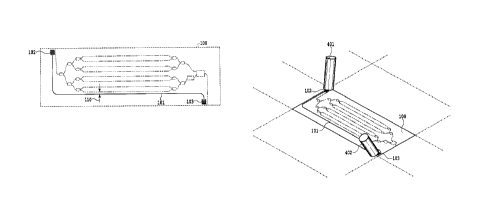
[0065] Fig. 14 is a diagram illustrating a method of an optical
circuit inspection during a process using the optical circuit of the
- 34 -
CA 03005704 2018-05-17
fourth embodiment of the present invention. The pair of grating
couplers 4102 which are light input/output mechanisms adjacently
arranged together is employed to schematically show a method of
measuring the light transmittance characteristic of the optical
waveguide 4101 in the state of a wafer.
[0066] In Fig. 14, the optical modulation circuit of Fig. 13 which
is a target circuit is shown in one rectangular area defined with
dotted lines, and each of a plurality of rectangular areas is aligned
on the wafer in the state before being cut out into one chip. Above
the pair of grating couplers 4102 arranged in parallel for the optical
circuit of the present invention, optical probes 4201 in which optical
fibers are fixed in parallel at a certain interval are disposed
proximate to each other for optical coupling. When connecting one
optical fiber of the optical probes 4201 to the light source for
measurement and the other optical fiber to a detector, light
transmittance characteristics of the optical circuit for inspection
can be evaluated as in the case of inputting/outputting light to/from
the end face of the substrate after being cut and separated into a
chip as in the conventional technique, and further, as in the
descriptions regarding the first embodiment in Fig. 4.
[0067] A pitch between two optical fibers of the optical probes
4201, that is, an interval between the pair of grating couplers 4102
depends on the design of an inspection device, but in consideration
of the covering diameter of the optical fiber, they should desirably
be located as close as possible in terms of positional accuracy. Here,
the pitch between the two optical fibers for the optical probes 4201
refers to a distance between the centers of the cores of the two optical
fibers, and the interval between the pair of grating couplers 4102
- 35 -
CA 03005704 2018-05-17
refers to a distance between the centers of the two rectangular grating
couplers.
[0068] Fig. 15 is a graph showing, in optical fiber block
components to which two optical fibers are fixed, a nominal value
of a pitch between fibers and an error amount of a pitch between
actually fabricated ones. In the optical fiber block components to
which two optical fibers are fixed at a specific pitch, a pitch between
the actually fabricated optical fiber block components is deviated
from a design value, that is, a nominal value of a pitch between the
optical fibers, and has variations. In Fig. 15, a horizontal axis
indicates nominal values and a vertical axis indicates errors of
actually fabricated pitches from nominal values. Normally, since the
mode field diameter of light in the optical fiber is approximately
j.im, a positional deviation between the grating coupler and the
optical fiber is required to be 0.5 Jim or less for making good optical
coupling. At this time, a pitch error allowed between the two optical
fibers is 1 tim, and as shown in Fig. 15, it is appropriate that a pitch
between the two optical fibers be 1 mm at most.
[0069] In the present embodiment, a method of detecting a flaw
on the optical circuit using light transmittance characteristics
obtained from the inspection during the manufacturing process of the
optical circuit is completely identical to those of the above
embodiments, and thus, its explanation will be omitted.
[0070] As described above, according to the optical circuit of
the present embodiment, a flaw occurred in the manufacturing process
of the silicon optical circuit on a wafer can be objectively detected
in an earlier stage in the inspection in the state of a wafer. In
the present embodiment, by making optical coupling of the grating
- 36 -
CA 03005704 2018-05-17
couplers more stable using a single optical probe, the detection and
judgment of a flaw on the optical circuit can be achieved more stably
and accurately compared to those in the first to fourth embodiments.
(Fifth Embodiment)
[0071] Fig. 16 is a plan view showing a configuration of an optical
circuit according to the fifth embodiment of the present invention.
In Fig. 16, a rectangular area defined by dotted lines shows a silicon
optical circuit chip 5100, which is composed of a circuit completely
identical to integrated circuits of an optical modulator and receiver
of a conventional technique as illustrated in Fig. 28. The silicon
optical circuit chip 5100 is also one chip area on a silicon wafer,
and further is a single optical circuit chip when being cut into chips
from the wafer. In Fig. 16, the optical modulator and receiver having
a configuration identical to the conventional technique is shown with
dotted lines, and an explanation on a configuration and operation
will be omitted. The optical modulator and receiver shown with the
dotted lines in Fig. 16 is a target circuit for implementing a
predetermined function which is to be a target of flaw detection.
[0072] The optical circuit of the present embodiment includes,
in addition to the optical modulator and receiver which are target
circuits depicted with the dotted lines in Fig. 16, an optical circuit
for inspection depicted with a solid line. The optical circuit for
inspection is composed of an optical waveguide 5101, 5102, 5103 and
a pair of grating couplers 5104 connected to both ends of the optical
waveguides 5101, 5103. A configuration of each of the pair of grating
couplers 5104 is identical to those of the first to fourth embodiments,
and further, the two grating couplers are proximately arranged
together as in the fourth embodiment.
- 37 -
CA 03005704 2018-05-17
[0073] In the present embodiment, as in the second to fourth
embodiments, the optical waveguide is arranged so as to surround the
target circuit, and particularly, since the target circuit is an
integrated circuit made of a plurality of sub target circuits (optical
modulator and receiver), the optical waveguide having a plurality
of loopback portions 5101, 5102, 5103 is arranged so as to surround
each of the sub target circuits. When a target circuit in an area
to be cut out into one chip has at least two circuit portions having
different functions, the sub target circuits refer to such circuit
portions. Since the sub target circuits have different functions,
it is possible to arrange them apart from each other on the chip,
and, as the case may be, it is even preferable to arrange them apart
from each other. In the case of including two or more sub target
circuits as in the present embodiment, an optical waveguide for
detection 5102 can be arranged so as to surround the contour of each
of the sub target circuits by extending over both of the two sub target
circuits through a space between the two sub target circuits.
[0074] In the present embodiment, the optical waveguide for
detection is composed of three waveguide portions, that is, a first
one is a loopback waveguide portion arranged along the upper side
of the contour of an optical modulator circuit (first sub target
circuit), a second one is a waveguide portion 5102 between the
above-described two sub target circuits, and a third one is a loopback
waveguide portion 5103 arranged along the lower side of the contour
of the receiver (second sub target circuit). The actual optical
waveguide for detection of Fig. 16 in the present embodiment is an
integrated optical waveguide in which the three waveguide portions
5101, 5102, 5103 of the arranged optical waveguide are arranged
- 38 -
CA 03005704 2018-05-17
continuously in series, and thus, there is no need to fabricate a
different waveguide separately and make them connect to each other.
At both ends of the integrated optical waveguide composed of the three
waveguide portions 5101, 5102, 5103 of the optical waveguide, the
two of the pair of grating couplers 5104 are provided.
[0075] The configuration of the present embodiment is also
applicable similarly to the case of three or more sub target circuits.
In other words, the optical waveguide for detection may at least
include a loopback waveguide portion arranged along a portion of the
contour of the sub target circuit located on the end part within the
chip and a waveguide portion between the sub target circuits arranged
along the contour of those sub target circuits by extending over two
or more different sub target circuits. A manner of configuring the
integrated optical waveguide as to in what order and in what way the
loopback waveguide portion and the waveguide portion between the sub
target circuits are to be arranged can be selected in variety in
accordance with the configuration and arrangement of the sub target
circuits, and the present invention is not limited at all to the
configuration of Fig. 16. As in the present embodiment, by configuring
the loopback optical waveguide portion and the waveguide portion
between the sub target circuits to surround the respective contours
of the plural' ty of sub target circuits, the accuracy of flaw detection
can be increased even with a small flaw occurred only on part of the
sub target circuit area of a target circuit inside a chip.
[0076] Therefore, the optical circuit of the present embodiment
can be carried out, in which the target circuit includes at least
two sub target circuits having an identical function or different
functions, the optical waveguide for detection at least includes:
- 39 -
CA 03005704 2018-05-17
loopback waveguide portions 5101, 5103 having an outward portion
arranged along a contour of a first sub target circuit from one coupler
of a pair of grating couplers so as to surround the first sub target
circuit and a return portion arranged by returning substantially
parallel to the outward portion; and a waveguide portion 5102 between
the sub target circuits arranged continuously from the loopback
waveguide portion of the first sub target circuit along part of a
contour that is not surrounded by the loopback waveguide portion of
the contour of the first sub target circuit or along at least part
of a contour of a second sub target circuit that is different from
the first sub target circuit, and the pair of grating couplers are
formed proximate and parallel to each other such that their incident
angles face the same direction at the time of coupling to fiber
components.
[0077] In the present embodiment, the optical modulator and
receiver having different functions have been shown as examples of
two sub target circuits included in a chip of a target circuit, but
it is needless to say that the present embodiment can also be applied
to a case where a plurality of sub target circuits having the same
function are included in one chip. In other words, in a case where
the plurality of sub target circuits having the same function are
arranged apart from each other, a flaw occurred within a chip can
be detected by the waveguide portion 5102 between the sub target
circuits as shown in Fig. 16.
[0078] In the present embodiment as well, as in the third
embodiment and fourth embodiment, the core widths of the linear
portions of the optical waveguide 5101, 5102, 5103 are enlarged to
form a multimode waveguide so as to reduce the propagation loss. The
- 40 -
CA 03005704 2018-05-17
core widths of curved portions of the optical waveguide 5101, 5102,
5103 are 0.5 gm and the core widths of linear portions are 1.5 gm.
A portion connecting the linear portion and other portions has a
continuously transformed core width as a tapered waveguide, and the
length of each tapered waveguide is 15 gm.
[0079] As in the above first to fourth embodiments, it is desirable
that the optical waveguide 5101, 5102, 5103 be arranged as close as
possible to the outermost contour of the waveguide for each of the
sub target circuits in the target circuit within a range in which
light coupling does not occur. The appropriate adjacent interval
between the waveguide of the target circuit and the optical waveguide
for detection is 50 gm at most.
[0080] Further, in the present embodiment, the two grating
couplers are adjacently arranged together in the vicinity of one
corner location of a rectangular chip area as in the fourth embodiment.
The grating couplers are configured to achieve optical coupling more
stably using a single optical probe. An interval between the pair
of grating couplers 5104 depends on the design of an inspection device,
but in consideration of the covering diameter of the optical fiber,
they should desirably be located as close as possible in terms of
positional accuracy, and it is appropriate to have the interval of
1 mm at most.
[0081] In the present embodiment as well, a method of detecting
a flaw on the optical circuit using light transmittance
characteristics obtained from the inspection during the manufacturing
process of the optical circuit is completely identical to those of
the above embodiments, and thus, its explanation will be omitted.
- 41 -
CA 03005704 2018-05-17
[0082] As described above, according to the present embodiment,
a flaw occurred in the manufacturing process of the silicon optical
circuit on a wafer can be objectively detected in an earlier stage
in the inspection in the state of a wafer. Further, in the case where
a plurality of sub target circuits exist within a chip, the present
invention can also be applied to a more complicated large-scale
optical circuit than the optical circuit including only the single
target circuit by using an integrated optical waveguide for detection
in which the loopback waveguide surrounding respective sub target
circuits is sequentially connected in series.
(Sixth Embodiment)
[0083] Fig. 17 is a plan view showing a configuration of an optical
circuit according to the sixth embodiment of the present invention.
The optical circuits of the present invention in the above first to
fifth embodiments are configured to detect a flaw occurred on the
optical circuit by each chip area that includes a target circuit to
be cut out into individual chips afterwards. The present embodiment
presents a circuit configuration capable of detecting a flaw by
simultaneously inspecting a plurality of target circuits arranged
on a wafer and a method thereof so as to enable efficient flaw detection
over a plurality of chips.
[0084] In Fig. 17, rectangular areas defined with dotted lines
show silicon optical circuit chips 6100 to 6103, respectively, and
are composed of circuits completely identical to the integrated
circuits of an optical modulator and receiver of a conventional
technique described in Fig. 28. Each of the silicon optical circuit
chips 6100 to 6103 is also one chip area on a silicon wafer, and in
the case of cutting the wafer into a chip, it becomes a single silicon
- 42 -
CA 03005704 2018-05-17
optical circuit chip. In Fig. 17, optical modulators and receivers
having configurations identical to those of conventional techniques
are shown with dotted lines, and explanations of their configurations
and operations will be omitted. The optical modulators and receivers
shown with the dotted lines within the respective rectangular areas
in Fig. 17 are target circuits for implementing a certain function
to be a target of flaw detection.
[0085] The optical circuits of the present embodiment include,
in addition to the optical modulators and receivers which are target
circuits depicted with the dotted lines in Fig. 17, optical circuits
for inspection depicted with solid lines. The optical circuit for
inspection is, in a chip area 6100, composed of an optical waveguide
6104 arranged so as to surround the target circuit and a pair of grating
couplers 6108 connected to both ends of the optical waveguide 6104.
Further, in a chip area 6101, an optical waveguide 6105 arranged so
as to surround a target circuit and a pair of grating couplers 6109
connected to both ends of the optical waveguide 6105 are provided.
Similarly, in a chip area 6102, an optical waveguide 6106 arranged
so as to surround a target circuit and a pair of grating couplers
6110 connected to both ends of the optical waveguide 6106 are provided,
and further, in a chip area 6103, an optical waveguide 6107 arranged
so as to surround a target circuit and a pair of grating couplers
6111 connected to both ends of the optical waveguide 6107 are provided.
[0086] The above-described configuration of the optical circuit
for inspection in each chip is identical to that of the fifth
embodiment shown in Fig. 16. The present embodiment has features in
which four optical waveguides 6104 to 6107 in respective chip areas
are further arranged therealong and in which one common optical
- 43 -
CA 03005704 2018-05-17
waveguide for detection 6112 connected in series is disposed so as
to surround four chips in the order of the optical waveguide 6104,
the optical waveguide 6105, the optical waveguide 6107, and the
optical waveguide 6106. To both ends of the common optical waveguide
for detection 6112, a pair of grating couplers 6113a, 6113b are
connected. A configuration of each of the pair of grating couplers
6108, 6109, 6110, and 6111 is identical to those of the embodiments
described above.
[0087]
Therefore, the present embodiment includes the four
individual optical waveguides for detection arranged so as to surround
the four target circuits, respectively, and, in addition to the above,
one common optical waveguide for detection arranged along each of
the four target circuits in sequence. The present embodiment is
configured to measure transmission spectra or an insertion loss by
using the optical probes via the pair of grating couplers for each
of the optical waveguides for detection.
[0088] In the
present embodiment, since the target circuit within
each chip is an integrated circuit made of a plurality of sub target
circuits as in the fifth embodiment, an integrated optical waveguide
in which a loopback optical waveguide portion surrounding each of
the sub target circuits within one chip and a waveguide portion between
the sub target circuits are arranged in series and grating couplers
disposed at both ends thereof are configured. Due to this, the accuracy
of flaw detection can be increased even with a small flaw occurred
only on part of the sub target circuit area of the integrated target
circuit.
[0089]
Furthermore, as in the third embodiment, fourth embodiment,
and fifth embodiment, the core widths of the linear portions of the
- 44 -
CA 03005704 2018-05-17
optical waveguides are enlarged to form multimode waveguides so as
to reduce the propagation loss in the optical waveguides. The core
widths of curved portions of the optical waveguides are 0.5 m and
the core widths of linear portions are 1.5 m. Portions connecting
the linear portions and other portions have continuously transformed
core widths as tapered waveguides, and the length of each tapered
waveguide is 15 m.
[0090] Further, in the present embodiment as well, it is desirable
that, as in all the embodiments described above, each optical
waveguide be arranged as close as possible to the outermost contour
of each of the sub target circuits in the target circuit within a
range in which light coupling does not occur. Each appropriate
adjacent interval between the waveguide of the target circuit and
the optical waveguide for detection is 50 m at most.
[0091] Moreover, in the present embodiment, as in the fourth
embodiment and fifth embodiment, in the pair of grating couplers 6108,
6109, 6110, and 6111, two grating couplers are adjacently arranged
together in the vicinity of one corner of each rectangular area of
a chip area. The pair of grating couplers 6113a, 6113b for the common
optical waveguide for detection 6112 is arranged at a corner of the
chip area 6102 in Fig. 17, but may be arranged on any chip within
the four chip areas. All of the pair of grating couplers are configured
to achieve optical coupling more stably with respective single optical
probes. An interval between the two grating couplers depends on the
design of an inspection device, but in consideration of the covering
diameter of the optical fiber, they should desirably be located as
close as possible in terms of positional accuracy, and it is
appropriate to have the interval of 1 mm at most.
- 45 -
CA 03005704 2018-05-17
[0092] Next, in the optical circuits of the present embodiment,
a method of detecting a flaw more efficiently on the optical circuits
using light transmittance characteristics obtained from the
inspection during the manufacturing process of the optical circuits
will be explained. In the above first to fifth embodiments, the
detection and judgment of a flaw on the optical circuits are made
separately for individual chip area at a time. In contrast, in the
present embodiment, the detection and judgment of a flaw on the optical
circuits are made for a plurality of chip areas, and, as required,
the detection and judgment of a flaw on the optical circuits are made
separately one by one for the individual chip areas. In other words,
hierarchical flaw detection and judgment which is composed of the
flaw detection and judgment using the common optical waveguide for
detection and the flaw detection and judgment using individual optical
waveguides for detection are made.
[0093] Fig. 18 is a diagram showing a state in which a scratch
has occurred on one optical circuit among target circuits during the
manufacturing process according to the optical circuits of the sixth
embodiment. In the optical circuits of the present embodiment shown
in Fig. 17, an example in which a flaw 6200 occurs on part (optical
modulation circuit) of a target circuit in a chip area 6103 during
the manufacturing process of the optical circuits is illustrated.
Here, by simply depicting the common optical waveguide for detection
6112 and the individual optical waveguides for detection 6104 to 6107
of the present embodiment shown in Fig. 17, hierarchized flaw
detection and judgment may be understood more easily.
[0094] Fig. 19 is a diagram schematically showing a hierarchical
configuration of the optical waveguides for detection according to
- 46 -
CA 03005704 2018-05-17
the optical circuits of the sixth embodiment of the present invention.
This diagram corresponds to the state of a flaw shown in Fig. 18,
and illustrates an example in which the flaw 6200 occurs on part
(optical modulation circuit) of the target circuit in the chip area
6103. The individual optical waveguides for detection 6104 to 6107
each exists only in one corresponding chip area so as to detect only
a flaw occurred on the optical circuit within one corresponding chip
area. In contrast, the common optical waveguide for detection 6112
is one optical waveguide configured to extend over the four chips,
and if a flaw exists in one of the optical circuits within the four
chip areas, this can be detected. On the other hand, if no flaw is
judged to exist in the common optical waveguide for detection 6112,
single inspection using one optical waveguide for detection 6112
allows simultaneous confirmation that no flaw exists within the four
chip areas.
[0095] In the optical circuits of the present embodiment, flaw
detection in the optical circuits is made in the following steps.
As a first measurement, the transmission spectrum of the common
optical waveguide 6112 arranged so as to continuously surround the
four target circuits is measured via the pair of grating couplers
6113a, 6113b. In a case where a flaw occurs on any of the four target
circuits, a great loss arises in the flaw (defect) occurred on the
common optical waveguide 6112, and thus, such a loss is also reflected
on the transmission spectrum measured by the common optical waveguide
6112.
[0096] Fig. 20 is a graph showing transmission spectra obtained
in cases with/without a flaw according to the optical circuits of
the sixth embodiment. In the case where the flaw 6200 occurs in one
- 47 -
CA 03005704 2018-05-17
of the target circuits as shown in Fig. 18, the transmission spectrum
of "with flaw" is obtained in Fig. 20. Meanwhile, in the case where
no flaw exists in any of the four target circuits as shown in Fig.
17, the transmission spectrum of "normal" is obtained in Fig. 20.
In the case where the "normal" transmission spectrum is obtained in
the first measurement and no flaw is detected in the common optical
waveguide 6112, the four target circuits are judged to have no flaw
at all, and the inspection during the manufacturing process for these
four chip areas is judged as passed, thereby completing the flaw
detection and judgment and then advancing to the process of other
subsequent four chip areas.
[0097] In the case where the "with flaw" transmission spectrum
is obtained in the first measurement and a flaw is judged to exist,
the process advances to a second measurement. In the second
measurement, the transmission spectra of the individual optical
waveguides 6104 to 6107 which are arranged so as to only surround
respective four target circuits are measured via the respective pair
of grating couplers 6108 to 6111.
[0098] Fig. 21 is a graph showing transmission spectra in four
measured target circuits in the second measurement according to the
sixth embodiment. Fig. 21(a) is a spectrum measured by the pair of
grating couplers 6108 in the chip area 6100 including a target circuit,
and similarly, Fig. 21(b) shows a spectrum measured by the pair of
grating couplers 6109 in the chip area 6101, Fig. 21(c) shows a
spectrum measured by the pair of grating couplers 6110 in the chip
area 6102, and Fig. 21(d) shows a spectrum measured by the pair of
grating couplers 6111 in the chip area 6103. In the case where the
flaw 6200 occurs on the single chip area 6103 of the target circuit
- 48 -
CA 03005704 2018-05-17
as shown in Fig. 18, a great loss is found on the transmission spectrum
of the optical waveguide that corresponds to the target circuit having
the flaw as in Fig. 21(d). By performing the second measurement, the
target circuit having the flaw can be specified and detected. If it
is possible to presume that a flaw exists in one location among the
four target circuits based on a transmission loss value obtained in
the first measurement, there is no need to perform the second
measurement to all the four target circuits. It is also possible to
stop the second measurement at a stage in which the target circuit
having the flaw is discovered. For instance, in the case where the
flaw is judged to exist on one location in the first measurement and
the flaw is specified by an initial measurement of the target circuit
in the second measurement, it is possible to omit inspection on the
subsequent three remaining target circuits. As a result, flaw
inspection for the four target circuits only requires two
measurements.
[0099]
Normally, it is a rare phenomenon that a flaw occurs on
the optical circuits in which a plurality of chip areas are arranged
within a wafer, and its frequency is in the level of being detected
on several circuits per wafer or not being detected at all. Under
such frequency of occurrence, inmost of the cases, no flaw is judged
to exist in the first measurement in the present embodiment, and as
in the first to fifth embodiments, the number of measurements can
be reduced by about one quarter compared to the case of detecting
a flaw by measuring the individual optical waveguides for detection
arranged along the contour of the target circuit for each of all the
chip areas.
- 49 -
CA 03005704 2018-05-17
[ 0 1 0 0 As in the present embodiment, the hierarchical detection
method by combining the measurement of the common optical waveguide
for detection and the measurement of the individual optical waveguides
for detection allows significant reduction in inspection time for
detecting a flaw occurred on the optical circuit to realize efficient
manufacturing and testing processes. In the above explanations of
the present embodiment, the common optical waveguide for detection
6112 is configured to extend over the four chip areas, the number
of chip areas through which the common optical waveguide for detection
passes can be appropriately changed according to the scale of an
optical circuit within one chip or the size of a chip. Therefore,
when increasing the number of chip areas through which the common
optical waveguide for detection passes, the number of target circuits
for detecting a flaw by the first measurement will be increased. If
a manufacturing process has less frequency of flaw occurrence, the
number of measurements required for one wafer can be reduced in inverse
proportion to the number of chip areas.
[0101] As described above, according to the present embodiment,
a flaw occurred during the manufacturing process of the silicon
optical circuit on the wafer can be objectively detected in an earlier
stage in the inspection in the state of a wafer. By making hierarchical
inspection using the common optical waveguide for detection which
is formed over the plurality of target circuits and the individual
optical waveguides for detection, the number of measurements of
transmission spectra can be significantly reduced to realize flaw
detection process with enhanced efficiency.
(Seventh Embodiment)
- 50 -
CA 03005704 2018-05-17
[0102] Fig. 22 is a plan view showing a configuration of optical
circuits according to the seventh embodiment of the present invention.
In the present embodiment as well, a circuit configuration capable
of detecting a flaw with fewer measurements by simultaneously
inspecting a plurality of target circuits arranged on a wafer and
a method thereof so as to enable efficient flaw detection over a
plurality of chips. In the present embodiment, by including optical
circuits for inspection in which wavelength bands to acquire
transmission spectra are divided by each target circuit, the number
of coupling locations to the grating couplers is reduced and the number
of measurements for flaw detection is significantly reduced to further
enhance efficiency of the flaw detection and judgment process for
a wafer.
[0103] In Fig. 22, rectangular areas defined with dotted lines
show silicon optical circuit chips 7100 to 7103, respectively, and
are composed of circuits completely identical to the integrated
circuit of an optical modulator and receiver of a conventional
technique described in Fig. 28. Each of the silicon optical circuit
chips 7100 to 7103 is also one chip area on a silicon wafer, and in
the case of cutting the wafer into a chip, it becomes a single silicon
optical circuit chip. In Fig. 22, optical modulators and receivers
having configurations identical to those of conventional techniques
are shown with dotted lines, and explanations of their configurations
and operations will be omitted. The optical modulators and receivers
shown with the dotted lines within the respective rectangular areas
in Fig. 22 are target circuits for implementing a certain function
to be a target of flaw detection.
- 51 -
CA 03005704 2018-05-17
[0104] The optical circuit of the present embodiment includes,
in addition to the optical modulators and receivers which are target
circuits depicted with the dotted lines in Fig. 22, optical circuits
for inspection depicted with solid lines. As individual optical
circuits for inspection for respective four chip areas, a chip area
7100 includes an optical waveguide 7104 which is arranged to surround
a target circuit, a chip area 7101 includes an optical waveguide 7105
which is arranged to surround a target circuit, a chip area 7102
includes an optical waveguide 7106 which is arranged to surround a
target circuit, and a chip area 7103 includes an optical waveguide
7107 which is arranged to surround a target circuit. In the present
embodiment, the optical circuits for inspection further include
wavelength multiplex/demultiplex circuits 7108, 7109 having a
function of branching light into four outputs according to wavelengths.
The optical waveguides 7104 to 7107 for inspection are each arranged
such that its one end is connected to one output of a first wavelength
multiplex/demultiplex circuit 7108 and the other end is connected
to one output of a second wavelength multiplex/demultiplex circuit
7109. One input of the first wavelength multiplex/demultiplex circuit
7108 and one input of the second wavelength multiplex/demultiplex
circuit 7109 are connected to a pair of grating couplers 7110,
respectively. A configuration of the pair of grating couplers 7110
is identical to that of each of the above embodiments.
[0105] In the circuits for inspection of the present embodiment
of Fig. 22, the four optical waveguides 7104 to 7107 which are arranged
so as to surround respective contours of the target circuits within
the four chip areas are configured so as to be branched from and merged
into the two wavelength multiplex/demultiplex circuits 7108, 7109
- 52 -
CA 03005704 2018-05-17
and so that transmission spectra can be measured with optical probes
via the single pair of grating couplers 7110. This is contrastive
to the case of the sixth embodiment shown in Fig. 17 in which the
chip areas include individual pairs of grating couplers 6108 to 6111,
respectively.
[0106] Further, in the present embodiment, each of the target
circuits is an integrated circuit made of a plurality of sub target
circuits as in the fifth embodiment and sixth embodiment. Due to this,
the integrated optical waveguides 7104 to 7107 in which, in each of
the target circuits, a loopback optical waveguide portion surrounding
each sub target circuit and a waveguide portion between the sub target
circuits are arranged in series are configured. In the present
embodiment, the four optical waveguides 7104 to 7107 are configured
to be connected to the two wavelength multiplex/demultiplex circuits
7108, 7109, and are connected to the single pair of grating couplers
7110 via the two wavelength multiplex/demultiplex circuits. Due to
the configuration of the present embodiment, even a small flaw
occurred only on part of the sub target circuit area of the integrated
circuit within each chip area can be detected with higher accuracy,
and at the same time, the number of pair of grating couplers required
is only one.
[0107] In the present embodiment as well, as in the third
embodiment, fourth embodiment, and fifth embodiment, the core widths
of the linear portions of the optical waveguides are enlarged to form
multimode waveguides so as to reduce the propagation loss. The core
widths of curved portions of the optical waveguides are 0.5 pm and
the core widths of linear portions are 1.5 p.m. Portions connecting
the linear portions and other portions have continuously transformed
- 53 -
CA 03005704 2018-05-17
core widths as tapered waveguides, and the length of each tapered
waveguide is 15 Rm.
[0108] As in the above first to sixth embodiments, it is desirable
that, the optical waveguides 7104 to 7107 be arranged as close as
possible to the outermost contour of the waveguide for each of the
sub target circuits in the target circuit within a range in which
light coupling does not occur. The appropriate adjacent interval
between the waveguide of the target circuit and the optical waveguide
for detection is 50 pm at most.
[0109] Moreover, in the present embodiment, as in the fourth
embodiment and fifth embodiment, the pair of grating couplers 7110,
that is, the two grating couplers are adjacently arranged together
in the vicinity of one corner of the rectangular chip area 7102. In
Fig. 23, the pair of grating couplers 7110 and the two wavelength
multiplex/demultiplex circuits 7108, 7109 are arranged on the lower
left part of the chip area 7102, but they may be located anywhere
within the four chip areas. The pair of grating couplers is configured
to achieve optical coupling more stably with a single optical probe.
An interval between the two grating couplers depends on the design
of an inspection device, but in consideration of the covering diameter
of the optical fiber, they should desirably be located as close as
possible in terms of positional accuracy, and it is appropriate to
have the interval of 1 mm at most.
[0110] Next, in the optical circuits of the present embodiment,
a method of detecting a flaw on the optical circuit more efficiently
using light transmission spectra obtained by the inspection of the
optical circuits will be explained. In the above first to fifth
embodiments, the detection and judgment of a flaw on the optical
- 54 -
CA 03005704 2018-05-17
circuits are made separately for individual chip area at a time. In
contrast, in the present embodiment, the detection and judgment of
a flaw on the optical circuits are simultaneously made by supplying
test lights which have been wavelength branched via the two wavelength
multiplex/demultiplex circuits 7108, 7109 to the four optical
waveguides 7104 to 7107.
[0111] Fig. 23 is a diagram showing a state in which a scratch
has occurred on one optical circuit among target circuits during the
manufacturing process according to the optical circuits of the seventh
embodiment. Here, an example in which a flaw 7200 occurs on part
(receiver) of the target circuit in the chip area 7101 is illustrated.
[0112] Fig. 24 is a graph showing demultiplexing characteristics
of the wavelength multiplex/demultiplex circuit according to the
optical circuits of the seventh embodiment. The respective
transmission spectra from an input port to the four output ports are
shown. Several optical circuits are considered for implementing a
wavelength multiplexing/demultiplexing function, but in the present
embodiment, an array waveguide diffraction grating is employed. The
array waveguide diffraction grating using a silicon waveguide is
disclosed in detail in NFL 1. Fig. 24(a) shows transmission spectra
for the first wavelength multiplex/demultiplex circuit 7108, and Fig.
24(b) shows transmission spectra for the wavelength
multiplex/demultiplex circuit 7109. The two wavelength
multiplex/demultiplex circuits 7108, 7109 in the optical circuits
of the present embodiment have the same design, that is, an interval
between multiplexing/demultiplexing wavelengths in design is 8 nm,
and a center wavelength of each output port is 1531 nm, 1539 nm, 1547
nm, and 1555 nm. However, due to machining errors and the like at
- 55 -
CA 03005704 2018-05-17
the time of actual manufacturing, a wavelength error of approximately
1 nm at maximum arises between the above-described design value and
the actual center wavelength.
[0113] In order to achieve detection of a flaw on the optical
circuit in the optical circuit of the present invention, an interval
between multiplexing/demultiplexing wavelengths for the wavelength
multiplex/demultiplex circuits 7108, 7109 is not limited to the above
value, and may be set to an arbitrary wavelength value. However,
considering the machining error at the time of the above-described
manufacturing, it is desirable that an interval between wavelengths
be set to larger than 1 nm. Further, it is desirable that the center
wavelengths of all the output ports fall within the range of a
wavelength region (about 40 nm) whose coupling efficiency between
the single pair of grating couplers 7110 and the optical fiber is
relatively favorable. Also, the wavelength multiplex/demultiplex
circuit used in the present embodiment is not limited only to the
array waveguide diffraction grating, but may also be applied to a
circuit having a wavelength multiplexing/demultiplexing function
such as Mach-Zehnder interferometer circuit (NPL 2) and a ring
resonance circuit (NPL 3).
[0114] Therefore, the optical circuit of the present embodiment
can be carried out as an optical circuit comprising: a plurality of
optical waveguides 7104 to 7107, each of which is for one of a plurality
of target circuits formed on the substrate, arranged along at least
part of a contour of each of the target circuits and arranged proximate
at a distance that does not cause optical coupling with each of the
target circuits; a first wavelength multiplex/demultiplex circuit
7108 in which one end of each of the plurality of waveguides is
- 56 -
CA 03005704 2018-05-17
connected to each of a plurality of output ends and in which light
input to the input end is wavelength multiplexed/demultiplexed to
the plurality of output ends; a second wavelength
multiplex/demultiplex circuit 7109 in which the other end of each
of the plurality of waveguides is connected to each of a plurality
of output ends and in which light input to the input end is wavelength
multiplexed/demultiplexed to the plurality of output ends, wherein
the second wavelength multiplex/demultiplex circuit includes
wavelength multiplexing/demultiplexing characteristics identical to
those of the first wavelength multiplex/demultiplex circuit, each
of the plurality of optical waveguides connected to the respective
output ends having the same transmissible wavelength on the two
wavelength multiplex/demultiplex circuits; and a pair of grating
couplers 7110 connected to the input end of the first wavelength
multiplex/demultiplex circuit and the input end of the second
wavelength multiplex/demultiplex circuit.
[0115] Fig.
25 is a diagram showing the connection relation
between two wavelength multiplex/demultiplex circuits and four
optical waveguides for detection according to the optical circuits
of the seventh embodiment. Both ends of the respective four optical
waveguides for detection 7104 to 7107 are connected to respective
output ports of the two wavelength multiplex/demultiplex circuits
7108, 7109 which are designed to have the same
multiplexed/demultiplexed wavelength. Here, the both ends of the
optical waveguide 7104 are connected to first output ports (Out #1)
on each of the two wavelength multiplex/demultiplex circuits, the
both ends of the optical waveguide 7105 to third output ports (Out
#3) on each of the two wavelength multiplex/demultiplex circuits,
- 57 -
CA 03005704 2018-05-17
the both ends of the optical waveguide 7106 to second output ports
(Out #2) on each of the two wavelength multiplex/demultiplex circuits,
and the both ends of the optical waveguide 7107 to fourth output ports
(Out #4) on each of the two wavelength multiplex/demultiplex circuits.
In addition, one input to the first wavelength multiplex/demultiplex
circuit 7108 and one input to the second wavelength
multiplex/demultiplex circuit 7109 are connected to the pair of
grating couplers 7110, respectively.
[0116] Several waveguide crossings occur among the optical
waveguides in Fig. 25, and it is desirable that a waveguide crossing
structure of a low loss be applied to these crossings. As there are
many publicly-known proposals on the low-loss waveguide crossing
structures, the structure represented in NPL 4, for example, may be
employed.
[0117] In the optical circuits of the present embodiment, in an
inspection during the manufacturing process for detecting a flaw
occurred on a target circuit, a transmission spectrum is measured
via the pair of grating couplers 7110 configured on a wafer by using
the optical probe. The test lights are supplied to the four optical
waveguides for detection via the two wavelength multiplex/demultiplex
circuits to measure transmission spectra.
[0118] Fig. 26 is a graph showing transmission spectra obtained
in cases with/without a flaw according to the optical circuits of
the seventh embodiment. In a case where a flaw occurs on any of the
four target circuits, among the optical waveguides 7104 to 7107, a
flaw (defect) occurred on the corresponding optical waveguide causes
a great loss, and thus, such a loss is reflected on the corresponding
wavelength region of the transmission spectrum. As shown in Fig. 23,
- 58 -
CA 03005704 2018-05-17
in the case where the flaw 7200 occurs on the target circuit (receiver)
in the chip area 7101, a loss arises on the optical waveguide 7105.
Accordingly, the loss caused by the flaw is reflected on a spectrum
in the vicinity of the wavelength of 1547 nm corresponding to the
third output ports (Out #3) on each of the wavelength
multiplex/demultiplex circuits 7108, 7109 to which the optical
waveguide 7105 is connected, and in Fig. 26, a transmission spectrum
indicated with a dotted line representing "with flaw" is obtained.
Meanwhile, in a case where no flaw exists on any of the four target
circuits, a transmission spectrum having the same loss level for all
the wavelengths corresponding to the respective four output ports
is obtained as indicated with a solid line representing "normal" in
Fig. 26.
[0119] Fig.
29A and Fig. 29B are diagrams showing another
implementing example of optical path conversion means in the present
invention. Optical conversion means can also be realized by an optical
circuit other than the grating couplers. Fig. 29A is a plan view
viewing the substrate face of the optical path conversion circuit.
Fig. 29B is a diagram showing a cross section that has been cut
vertically to the substrate face along the optical waveguide including
XXIXB-XXIXB line in Fig. 291\. In this embodiment, the silicon optical
circuit is to be shown as an example of implementing optical path
conversion means, but it is possible to implement the optical path
conversion means of approximately the same structure even with optical
circuits made of other material systems. With reference to Fig. 29A,
the optical path conversion circuit is configured at the end part
of a waveguide core portion 8101 which is part of the optical waveguide
for detection and which is formed of silicon. The waveguide core
- 59 -
CA 03005704 2018-05-17
portion 8101 corresponds to an optical waveguide 8105 in the sectional
view of Fig. 29B. With reference to Fig. 29B, in the vicinity of the
optical path conversion circuit, a BOX layer (lower part cladding)
8106 and further an upper part cladding 8104 made of SiO2 are formed
above a silicon substrate part 8107 of a SOT substrate. The waveguide
core portion 8105 has a thickness of 0.22 m and a width of 0.5 m,
the upper part cladding 8104 has a thickness of about 2 m, and the
lower part cladding 8106 has a thickness of 2 m.
[0120] The optical path conversion circuit of Fig. 29A includes
a groove portion 8102 formed by machining the upper part cladding
8104, the waveguide core portion 8105, and the lower part cladding
8106. The groove portion 8102 has two end faces which are vertical
to the optical waveguide 8105. Meanwhile, an end face terminating
one end face of the waveguide core 8105 is formed nearly vertical
to the silicon substrate 8107. Another end face 8103 facing the
terminating face is a total reflection face against light, and is
formed with an angle of about 45 degrees relative to the silicon
substrate 8107. The end face 8103 having the total reflection face
may be made of a material used for the upper part cladding and lower
part cladding, that is, the face made of SiO2, but may alternatively
be formed of a metal film or the like on a surface in order to obtain
higher reflection efficiency.
[0121] Here, a lightwave propagating through the optical
waveguide 9105 from the right side to the left side in Fig. 29B is
emitted into a free space in the groove portion 8102, and, before
long, reaches the total reflection face 8103, whereby its advancing
direction is converted nearly upward in Fig. 29B. Similarly, light
input from the upper part of Fig. 29B advances along a route opposite
- 60 -
CA 03005704 2018-05-17
of the above route to couple with the optical waveguide 9105 to be
propagated toward the right side of Fig. 29B. This optical path
conversion circuit enables light connection with input/output means
such as the optical fiber disposed at upper part of the groove portion
8102 in Fig. 29B. Therefore, the optical path conversion circuit
composed of the groove portion 8102 including the terminating face
of the optical waveguide and the total reflection face which faces
the terminating face and which reflects light emitted from the
terminating face substantially vertically relative to the SOI
substrate functions as a coupler that couples entering/outgoing light
with the optical fiber. At both ends of the optical waveguide for
detection in each of the above embodiments, the optical path
conversion circuit illustrated in Fig. 29A and Fig. 29B can be provided.
The above-described pair of grating couplers are replaceable with
the pair of couplers using the optical path conversion circuit
illustrated in Fig. 29A and Fig. 29B.
[0122] In the
optical circuits of the present embodiment of the
present invention, the presence/absence of a flaw in each of the four
target circuits can be simultaneously judged by one measurement.
Therefore, as in the above first to fifth embodiments, the number
of measurements are reduced by approximately one quarter and the
inspection time can be reduced when compared with the case of flaw
detection measurement by measuring the individual optical waveguide
corresponding to each of all the target circuits, thereby achieving
enhanced efficiency. Further, when compared with the optical circuits
of the sixth embodiment, the efficiency of the inspection is superior
in that the coupling between the grating couplers and the optical
- 61 -
CA 03005704 2018-05-17
probe is only required to be made on one location and that a target
circuit with a flaw can be specified by only one measurement.
[0123] In the above explanation of the present embodiment, the
four optical waveguides for detection 7104 to 7107 are arranged in
the corresponding four chip areas, and are merged into the two
wavelength multiplex/demultiplex circuits 7108, 7109. However, the
number of optical waveguides for detection to be merged into the two
wavelength multiplex/demultiplex circuits 7108, 7109, that is, the
number of target circuits (chip areas) for flaw detection can be
appropriately changed according to the scale of an optical circuit
within one chip or the size of one chip. Therefore, if the number
of optical waveguides for detection to be merged into the two
wavelength multiplex/demultiplex circuits 7108, 7109 can be increased,
the number of target circuits for detecting a flaw only by one
measurement can be increased. In this case, by narrowing a wavelength
interval within a range in which loss difference can be identified
and by increasing the number of ports of the wavelength
multiplex/demultiplex circuits, the number of target circuits for
discovering a flaw only by one measurement can be increased. If the
manufacturing process has less frequency of flaw occurrence and has
relatively less deficiency, in inverse proportion to the number of
optical waveguides for detection (chip regions) to be merged into
the two wavelength multiplex/demultiplex circuits 7108, 7109, the
number of whole measurements in one wafer can be reduced.
[0124] As described above, according to the present embodiment,
a flaw occurred in the manufacturing process of the silicon optical
circuits on a wafer can be objectively detected in an earlier stage
in the inspection in the state of a wafer.
- 62 -
CA 03005704 2018-05-17
[0125] As such, explanations have been given in detail that,
according to the optical circuits of seven embodiments of the present
invention, the silicon optical circuit for inspection during the
process of the present invention allows objective detection with
higher detection accuracy of a flaw occurred in the manufacturing
process of the optical circuit on a wafer compared to the visual
inspection of a conventional technique.
[0126] Explanations have been given that, in the first embodiment
to fourth embodiment, the optical modulation circuit of a digital
coherent polarization multiplexed system is employed for a target
circuit for detecting a flaw, and in the fifth embodiment to seventh
embodiment, the optical modulation circuit and optical reception
circuit are employed as the integrated circuit, but the present
invention is not limited to those target circuits, and may be applied
to all optical circuits that are composed of silicon optical
waveguides.
[0127] In all the embodiments, explanations have been given by
using configuration examples such that the upper part cladding and
the lower part cladding are made of quartz and that a specific value
is employed for a thickness, but the optical circuit of the present
invention is not limited to these examples. A material having a lower
refractive index than silicon is applicable to the cladding, and a
thickness of each cladding may sufficiently exceed the range of light
that slightly seeps out of the core, failing to be accommodated in
the core. Alternatively, it is also possible to clad air as the upper
part cladding instead of filling the core with a specific material.
[0128] Furthermore, in all the embodiments described above, the
design parameters of the grating couplers have been explained to have
- 63 -
CA 03005704 2018-05-17
specific values, but the optical circuit of the present invention
is not limited to these examples, and may be applied to the grating
couplers of any design. Moreover, in the embodiments of the present
invention, an example of the design of operating in a so-called C
band (the wavelength of approximately 1525 nm to 1565 nm) with high
efficiency has been presented, and it is desirable that the
appropriate design of grating couplers be applied in accordance with
the use of, for example, wavelengths for operating an optical circuit.
[0129] As described above, according to the optical circuit of
the present invention, a flaw occurred in the manufacturing process
of the silicon optical circuit on a wafer can be objectively detected
by inspection in the state of a wafer. Further, according to the
present invention, a flaw occurred in the manufacturing process of
the silicon optical circuits can be detected with high accuracy in
an earlier stage of the manufacturing process and can efficiently
prevent a circuit including failure which has been overlooked in
inspection in the state of a wafer from flowing out to subsequent
processes. The manufacturing time and cost for products that employ
silicon optical circuits can be reduced.
Industrial Applicability
[0130] The present invention can be used for a communication
system in general. In particular, the present invention can be used
for a silicon optical circuit of an optical communication system.
- 64 -