Note: Descriptions are shown in the official language in which they were submitted.
1
PROPERTIES OF A SURFACE AND SUBSURFACE STRUCTURES WITH WHITE
LIGHT INTERFEROMETRY USING PHOTONIC JETS
Field of the invention
Low coherence interferometry (LCI), particularly Scanning White Light
Interferometry
(SWLI), is a widely used 3D surface characterization method featuring sub-
nanometer
resolution in vertical direction. By combing SWLI with optical jet structures
one
achieves 3D super resolution imaging.
State of the art
Light sources for SWLI are halogen lamps or white-light light-emitting diodes
(LED)
imaged into the objective pupil in a Kohler geometry. The illumination field
and
aperture are controlled. The light source may be stroboscopic to freeze
oscillating
motion, and the emission spectrum may be electronically controllable. The
source
wavelengths are visible or infrared (1-2 or 10 pm).
Area imaging sensor camera (CCD, CMOS) for SWLI has from 640 x 480 pixels to
40+ million pixels. Camera selection involves field size and number of pixels
as well
as acquisition speed, response linearity, quantum well depth, and digitization
resolution.
Reference surface/mirror (Michelson type interferometer configuration) is
aluminized
glass, silicon carbide (SIC), or bare glass, depending on sample reflectivity.
The mirror
in a Mirau type interferometer configuration is a small metallic coating,
slightly larger
in diameter than the field of view, on a transparent reference plate.
The optical system of a LCI device employs infinite conjugate optics with
telecentric
imaging, and magnification determined by the combined action of the objective
and
tube lens. The measurement principle requires engineering and adjusting the
objective so that the zero group-velocity optical path difference position is
identical
to the position of the best focus. The Michelson objective achieves this with
a
dispersion balanced cube beam splitter. In a Mirau microscope, the beam
splitter and
reference plate should match in optical thickness to minimize dispersion.
Date Recue/Date Received 2020-11-04
2
Lateral resolution can be determined e.g. in the following way. The Abbe
diffraction
limit (dx,y) is the smallest lateral periodicity in a structure, which can be
discriminated
in its image:
dx,y = 1.22A/2NA (1)
where A is the center wavelength of the light and NA is the numerical aperture
of the
lens. When imaging with visible light (A ¨ 400-750 nm) and commonly used
objectives
with NA = 1.4, the lateral resolution is approximately 200 nm.
The diffraction limit is due to loss of evanescent waves in the far field.
These
evanescent waves carry high spatial frequency sub-wavelength information of an
object and decay exponentially with distance.
The axial image resolution (di) is 2-3 times larger than the lateral
resolution, around
440 nm.
dz = 2nA/NA2 (2)
where n is the refractive index of the medium in which light propagates.
Any microscopy technique that overcomes the resolution limit by factor of 2 or
higher
is considered to provide super-resolution.
Scanning electron microscopes (SEM) can provide 3D nano-resolution images by
e.g.
using several electron guns or detectors simultaneously. These devices do not
provide
super resolution.
Low coherence interferometry, i.e. SWLI, overcomes the axial resolution limit
and
allows superior ¨resolution along the vertical direction (sub-nanometer).
Near field techniques offer lateral and vertical super-resolution. Optical
near-field
microscopy is based on measuring scattered light, close to a near-field probe,
which
is generated by optical near-field interaction between the nearfield probe and
a
specimen. Near-field probe tips of known shape are used to achieve high local
Date Recue/Date Received 2020-11-04
3
resolution, e.g. contacting atomic force microscope (AFM) and noncontacting
scanning tunneling microscope (STM) tips. The near-field probe can be
illuminated by
focused light to generate scattered light.
There are noncontacting techniques based on photonic nanojets that permit 50
nm
lateral resolution in the x-y plane but much worse axial resolution (z-
direction).
The photonic nanojet is a narrow, high-intensity, non-evanescent light beam
that can
propagate a distance longer than the wavelength A after emerging from the
shadow-
side surface of an illuminated lossless dielectric microcylinder or
microsphere of
diameter larger than A. The nanojet's minimum beamwidth can be smaller than
the
classical diffraction limit, in fact as small as ¨A/3 for microspheres.
US patent application 2010/0245816 Al describes near-field Raman imaging,
performed by holding a dielectric microsphere (e.g. of polystyrene) on or just
above
the sample surface in a Raman microscope. An illuminating laser beam is
focused by
the microsphere to produce near-field interaction with the sample. Raman
scattered
light at shifted wavelengths is collected and analyzed. The microsphere may be
mounted on an AFM cantilever or on some other scanning probe microscope that
provides feedback to keep it in position relative to the sample surface.
Alternatively,
the microsphere may be held on the sample surface by the optical tweezer
effect of
the illuminating laser beam. One disadvantage of this device is the vertical
resolution
which depends strongly on the confocal design of the Raman microscope being
used.
For a true confocal design (which incorporates a fully adjustable confocal
pinhole
aperture) depth resolution is on the order of 1-2 pm.
Probes of scanning near-field optical microscopes create electromagnetic field
characteristics that are maximally localized near a nano-sized point
(miniature
apertures and tips, fluorescent nano-particles and molecules, dielectric and
metal
corners). However, the probe field, which is distributed across a larger area,
can
provide super-resolution as well. For this purpose, the field spectrum should
be
enriched with high spatial frequencies corresponding to small dimensions of
the
sample. As examples of such nearfield probes, US patent 2009/0276923 Al
proposes
and theoretically studies models of optical fibers whose end-face features
sharp linear
edges and randomly distributed nanoparticles. These kinds of probes are
mechanically
Date Recue/Date Received 2020-11-04
4
more robust than conventional probes - fabricated by using a combination of a
two-
step chemical etching and focused ion beam milling and their manufacturing
does not
require nanoscale precision. The optical probes enable waveguiding of light to
and
from the sample with marginal losses by distributing and utilizing the
incident light
more completely than conventional probes. Numerical modeling shows that, even
with
substantial measurement noise, these probes can resolve objects that are
significantly
smaller than the probe size and, in certain cases, can perform better than
conventional nanoprobes. One disadvantage of this device is that it measures
point
by point.
Patent application document WO 2013/043818 Al describes a system and method
for
imaging a surface, including a nano-positioning device including a cantilever
with an
optically transparent microsphere lens coupled to the distal end of the
cantilever. An
optical component can focus light on at least a portion of the surface through
the
microsphere lens, and the focused light, if any, reflects back from the
surface through
the microsphere lens. A control unit communicatively coupled with the
nanopositioning device can be configured to position the microsphere lens at a
predetermined distance above the surface. One disadvantage of this device is
the
vertical resolution which is diffracted limited.
In far-field microscopy, imaging contrast is often low and unsatisfactory due
to out-
of-focus light in the final image. To enhance contrast, one can optimize the
microscope lighting condition and imaging software settings during imaging. In
contrast to far-field microscopy, confocal microscopy techniques generally
have better
optical contrast and improved resolution; this is achieved by placing a tiny
pinhole
before the detector to eliminate out-of-focus light in the final image. When
combining
laser confocal microscopy with micro-spheres, multiple concentric rings in the
confocal
imaging appears if one uses closely positioned spheres. These rings result
from near-
field interactions between the particle or spheres and the substrate under
coherent
laser illumination. In contrast, an incoherent light source, renders this
issue less
obvious in far-field microscopy. These rings degrade imaging quality, which
may pose
a practical limit on the minimum feature that can be resolved in confocal
imaging.
Prior art embodiments suffer from these artefacts that might wrongly be
interpreted
as objects in the image. For isolated and known particles, one can still see
the true
Date Recue/Date Received 2020-11-04
5
image of the objects through the particles. The artefact issue is less obvious
in a far-
field nanoscopy system where an incoherent lighting source is often used.
Prior art describes polarization as a way to enhance contrast especially in
bio-imaging.
There are many studies on polarization in far-field microscopy and also
several studies
on polarization-SWLI for both imaging static and moving samples. There are
some
studies on the use of polarization in near field microscopy but it has never
been used
in 3D super-resolution imaging. Prior art publications fails to present 3D
calibration
at the nanometer scale.
Short description of the invention
An object of the present invention is to achieve an improved 3D super
resolution
imaging system and method for determining surface topographies and/or
subsurface
structures. This is achieved by an arrangement for determining three-
dimensional
properties of an interface of an object, the arrangement comprising means for
interferometric imaging, wherein the means for interferometric imaging
comprises: a
light source, imaging means for forming an interference image based on
interference
between light arriving at the imaging means from the interface of the object
and light
arriving at the imaging means from a reference path related to the
interferometric
imaging, and means for forming the reference path from the light source to the
imaging means, for directing light from the light source towards the interface
of the
object, and for directing light from the interface of the object to the
imaging means,
wherein the arrangement further comprises means constituting a near field
modifying
structure for forming, from the light directed towards the interface of the
object, one
or more photonic jets directed to the interface of the object, wherein the
means for
interferometric imaging is arranged to perform the interferometric imaging
through
the means constituting the near field modifying structure.
An arrangement according to an exemplifying embodiment of the invention is an
arrangement for determining four-dimensional properties of an interface of an
object.
The arrangement comprises a light source, means for forming photonic jets to
be
utilized in imaging of the interface, means for performing large field of view
interferometric imaging of the interface and of a combination of the interface
and the
means for forming the photonic jets, means for passing said light being close
to the
Date Recue/Date Received 2020-11-04
6
interface and direct the light to the interface, and said means create an
image, and
the arrangement comprises means for performing phase shifting interferometric
imaging of the interface, imaging means for receiving light from the interface
modulated by at least one of microspheres and near field modifying structures
for
forming super-resolution image information by combining light interferometry
with
the photonic jets, and a processor unit for determining four-dimensional
properties of
the interface on the basis of the image information formed by said phase
shifting
interferometric imaging by utilizing the effect of the photonic jets.
An object of the invention is also a method for determining three-dimensional
properties of an interface of an object, the method comprising: directing
light from a
light source to a reference path related to interferometric imaging, directing
light from
the light source towards the interface of the object, and performing the
interferometric imaging so as to form an interference image based on
interference
between light arriving from the interface of the object and light arriving
from the
reference path, wherein the interferometric imaging is performed through means
constituting a near field modifying structure for forming, from the light
directed
towards the interface of the object, one or more photonic jets directed to the
interface
of the object.
A method according to an exemplifying embodiment of the invention is a method
for
determining four-dimensional properties of an interface of an object. In the
method
is produced light, is formed photonic jets to be utilized in imaging of the
interface, is
performed large field of view interferometric imaging of the interface and of
a
combination of the interface and the means for forming photonic jets, is
passed said
light close to the interface and is directed the light to the interface, and
is created an
image, and is performed phase shifting interferometric imaging of the
interface, is
received light from the interface modulated by at least one of microspheres
and near
field modifying structures for forming super-resolution image information by
combining light interferometry with the photonic jets, and is determined four-
dimensional properties of the interface on the basis of the image information
formed
by said phase shifting interferometric imaging by utilizing the effect of the
photonic
jets.
Date Recue/Date Received 2020-11-04
7
The invention is based on photonic jets which are utilized in imaging of the
interface,
and on performing large field of view interferometric imaging of the interface
and a
combination of the interface and the means for forming the photonic jets.
Light is
passed close to the interface and is directed to the interface, and is created
an image.
The invention can be further based on phase shifting interferometric imaging
of the
interface, and on light received from the interface modulated by microspheres
for
forming super-resolution image information by combining light interferometry
with
the photonic jets.
A benefit of the invention is that label free, noncontact, large field of view
and fast
determination of four-dimensional properties of an interface of an object can
be
achieved.
Short description of figures
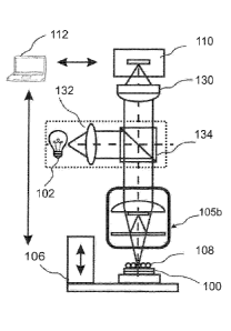
Figure 1 presents first exemplary embodiment according to the present
invention.
Figure 2 presents second exemplary embodiment according to the present
invention.
Figure 3 presents preferred embodiment according to the present
invention.
Figure 4 presents an example of a surface imaged according to the
invention.
Detailed description of the invention
According to the present invention can be achieved non-contacting large field
of view
3D super-resolution imaging by combining light interferometry for the z axis
and
photonic jet for the xy-plane. The light interferometry can be e.g. so called
white light
interferometry. The z axis imaging uses a real image, injects light into the
near-field
modifying structure, e.g. a sphere, and extracts through the sphere light
reflected
from the interface. In the xy plane imaging is injected light into the sphere,
is
Date Recue/Date Received 2020-11-04
8
extracted light through the sphere and from outside of the sphere, and is used
a
virtual image of the interface.
In figures 1, 2, and 3 are presented exemplary preferred embodiments according
to
the invention, in which an arrangement for determining four-dimensional
properties
of an interface 100 of an object comprises a light source 102. Four
dimensional means
3D (xyz dimensions) and time domain. The interface 100 can be a surface of the
object or a subsurface of the object, i.e. a so called buried surface. The
arrangement
comprises means for forming photonic jets to be utilized in imaging of the
interface
100 and means 105a,b for performing large field of view interferometric
imaging of
the interface 100 and of a combination of the interface and the means for
forming
the photonic jets. In one embodiment the arrangement can comprise means for
performing image stitching to stitch either separately or together both
superstructure
and substructure to have large field of view. The means for forming photonic
jets can
comprise at least one of a microsphere and micro cylinder and micro-lense
(e.g.
Fresnel) and grid and cubes and metamaterials and negative refractive index
materials, as well as any near-field modifying structure of a specified and
known
shape or of an unspecified shape when one can use a known target to extract a
so
called point spread function. Also the means for forming photonic jets can
comprise
e.g. polymer or polymer-like material with photonic jets. The photonic jets
can be e.g.
nanojets or equivalents. In one embodiment the arrangement can also comprise
means for performing the measurements using polarized light.
The arrangement according to the invention comprises means 108 for passing
said
light that are close to the interface 100 and direct the light to the
interface, and create
an image, and means 106 for performing phase shifting interferometric imaging
of
the interface 100. The means 108 are preferably microspheres 108, which can be
e.g.
high-index microspheres 118 embedded partially or fully in a substantially
thin
transparent host material 116. In one embodiment means 106 for moving the
object
can be used as the means 106 for performing phase shifting interferometric
imaging
of the surface 100. The means 106 for moving the object can be e.g a glass
micropipette 114 attached to the microspheres 108 for moving the microspheres
108
and another tip to locally actuate the surface of the object, which is e.g.
cell. In
another embodiment the means 106 for performing phase shifting interferometric
imaging of the surface 100 can comprise utilization of stroboscopic
illumination.
Date Recue/Date Received 2020-11-04
9
The arrangement according to the invention further comprises imaging means 110
for receiving light from the interface 100 modulated by microspheres 108 for
forming
super-resolution image information by combining light interferometry with the
photonic jets, and a processor unit 112 for determining four-dimensional
properties
of the interface 100 on the basis of the image information formed by said
phase
shifting interferometric imaging by utilizing the effect of the photonic jets.
The
imaging means 110 can be e.g. a CCD camera. In figure 4 is presented an
example
of a surface 100 imaged according to the invention.
In one embodiment the arrangement can comprise means for performing same field
of view calibration on the basis of an improved nanoruler concept where one
has
added a grid to the lowest step in order to allow simultaneous z axis and xy
axis
calibration. The means can be e.g. a stack of Langmuir Blodgett films on e.g.
a
microscope glass. The grid can be created with e.g. short wavelength
lithography.
In another embodiment the arrangement can comprise means 124 for forming
coherence function to achieve minimum main lobe width and sufficient side lobe
reduction in order to remove impact of the photonic jet layer and to allow
maximum
resolution. The means 124 can be accomplished e.g. by using a light source
with
different coherence length or by using a rough disc to break the coherence of
the
light source or by combining in suitable way several light sources.
In one further embodiment the arrangement can comprise means 126 for managing
polarization to create at least one of phase shift, transient imaging, and
enhanced
image contrast. The means 126 can be accomplished e.g. by placing polarizer in
front
of the light source and an analyzer in front of the large area detector or by
using
pixelated polarizers.
In some embodiment according to the invention the arrangement can comprise
means for accounting for the distortion of the surface topography created by
the finite
size shape of the photonic jet. These means can be incorporated e.g. by
relying on
deconvolution approaches similar to those used to correct for the finite tip
size in AFM
imaging.
Date Recue/Date Received 2020-11-04
10
In the following is described more detailed features of the different
embodiments
according to the present invention. LCI (SWLI) and the photonic nanojet
technology
are combined to achieve 3D super-resolution featuring tenths of nanometers
lateral
and vertical resolution. This should provide voxels that are more equilateral
(symmetric) and smaller than previously achieved. The device permits label-
free non-
contacting imaging of both surfaces and buried structures that may be static
or may
move. The full field of view techniques provides fast and simultaneous view of
all
points on a fairly large area. Traceability of the image dimensions can be
achieved
using the nanoruler approach. The device, i.e. arrangement according to the
invention
can be hand held.
In one embodiment presented in figure 1 is used a SWLI setup with a Mirau
interference objective 105b. The nanojet can be achieved by using microsphere
or
micro cylinders or micro-lense or grid or cubes or metamaterials or negative
refractive
index materials or nanoparticles of a specified and known shape ¨ spherical,
hemi-
spherical or other shape to produce nanojets. In addition, a wetting layer,
serving as
a lubricant, could be used. Nanojet particles could be freely placed on the
sample or
embedded partly or entirely in the polymer material using e.g. self-assembly
technics,
forming single or multilayered structure. In the latter case attention should
be paid
to the thickness of the layer.
In another embodiment presented in figure 2 is used a Linnik or Michelson
configuration 105a, which allows use of different conventional objectives and
which
also permits layer thickness compensation in case polymers are used as an
embedding
material. It also allows subsurface imaging, i.e. imaging of buried
structures.
These embodiments in microscopy require control of the positioning of the
microspheres during scanning. Two approaches to solve this problem are: (1)
the
microsphere is moved with a fine glass micropipette attached to the
microsphere, (2)
high-index microspheres (TiO2 or BaTiO3) can be partly or fully embedded in a
transparent host material (e.g. PMMA, PDMS), having a thickness similar to a
standard
coverslip, which is thin enough for the micro-lens or near-field modifying
structure to
be directly inserted into the gap between a conventional microscope's
objective lens
and the sample. Preferred sizes of the microspheres is e.g. 10 micrometers
with
Date Recue/Date Received 2020-11-04
11
refractive index of the material being e.g. 1.6, and magnification of the
objectives
used in the arrangement is e.g. 50X.
The embodiments according to the present invention can be utilized e.g. in the
following applications:
I The invention can be utilized in drug development. It helps high-throughput
screening. It helps development of personalized treatment cocktails at the bed
side
for cancer treatment. It is a physical way of doing dissolution tests on
complex drug-
carrying drug-delivery devices. With this super-resolution technique one can
precisely
measure erosion of the drug delivery devices. This means that one does not
have to
carry out chemical dissolution tests that can be slower and that may require
more
substance for the tests. Moreover, the same approach can be used for any kind
of
nanochemistry-like approach where one either adds nanoparticles to a surface
or to
a construct or remove them either actively or passively.
II The invention can be utilized in tests of fibers and constructs produced by
ultrasound enhanced electrical spinning, - a way to produce drug-laden
nanofibers.
These fibers can be used e.g. in fiber constructs whose diameters are
controlled to
allow controlled release profiles. Such fibers could e.g. react to the
surrounding
glucose level and release insulin on demand.
In prior art the only way to image these nanoscale constructs is AFM or SEM,
which
are complex and slow.
III The invention allows one to rapidly take images of nanoparticles of size
below
one hundred nanometers. These kinds of nanoparticles can give existing failed
drug
components a second chance. It is important for quality assurance purposes to
see
these nanoparticles when you produce them. This cannot be done with SEM or
AFM,
because they are too slow.
IV According to the invention can be provided a tool for supersurface and
subsurface
bioimaging in a label free manner at nanometer resolution. Imaging using dyes
as
well as label free AFM imaging suffer according to prior art from serious
problems.
Date Recue/Date Received 2020-11-04
12
V According to the invention can be provided a read-out device for
security
applications where can be used embedded nanodots as a way to ensure
authenticity.
Although the invention has been presented in reference to the attached figures
and
specification, the invention is not limited to those as the invention is
subject to
variations within the scope allowed for by the claims according to different
kind of
applications.
Date Recue/Date Received 2020-11-04