Note: Descriptions are shown in the official language in which they were submitted.
CA 03006630 2018-05-28
1
CIRCUIT ARRANGEMENT FOR OPERATING ELECTROMAGNETIC DRIVE
SYSTEMS
The present invention relates to a circuit arrangement for actuating an
electromagnetic drive system for electromechanical devices as well as a method
for
operating a circuit arrangement for actuating an electromagnetic drive system
for
electromechanical devices.
Electromagnetic drive systems are often used in electrical engineering to
apply force
on movable mechanical components. Such systems use for example pull magnets or
other electromagnetically operative component assemblies. These drive systems
are
used inter alia in contactors, circuit breakers, relays, solenoid valves, etc.
in various
forms.
In the actuating of such drive systems, the magnetic system is usually
directly
energized by the control voltage source; an acceleration of mechanical
components
thereby occurs such as e.g. armature or lever systems. That causes, for
example,
the closing of switch contacts. However, the force curve and closing speed in
this
case depend on the amount of voltage applied.
Yet it is also known that the energy supply of drive systems is often
controlled by
electronic assemblies (ballasts) such that the displacement/time
characteristic of the
force curve optimally corresponds to the requirements of the mechanical system
during actuation
Already known from DE 20 2011 051 972 U1 is a circuit arrangement for
actuating a
switching device which exhibits a first switch position and a second switch
position
and can be switched between the first switch position and the second switch
position
and comprises at least one electromagnetic actuating device for generating a
actuating force for switching the switching device between the first switch
position
and the second switch position and a trigger circuit for actuating the
electromagnetic
actuating device.
CA 03006630 2018-05-28
2
The actuation of the aforementioned drive systems by directly loading the
magnetic
systems with the available control voltage has the disadvantage of the
supplied
control current and thus the magnetic force usually not being adapted to the
existing
force/ displacement characteristic of the powered mechanical system.
The known electronic ballasts for operating magnetic drive systems directly
clock the
magnetic systems via one or more electronic switches. Thereby disadvantageous
is
that while the available control voltage can be reduced, it cannot be
increased.
Yet it is advantageous in a number of applications of said drive systems to
also be
able to increase the actuation control voltage if needed. Otherwise in such
applications ¨ for example in undervoltage situations ¨ safe actuation is not
possible.
Furthermore, these ballasts preferably serve in the actuating of switching
devices in
the form of in contactors in which the power requirement is initially high but
which
then drops over time.
The direct clocking of the electrical drive system additionally results in an
interference voltage spectrum which can negatively affect other electronic
systems.
The pulse gradient also causes an increased loading of the coil structure of
the
magnetic systems which are mostly designed for DC or low-frequency AC
operation.
The clocked mode of operation can thus cause damage to the winding of the
magnetic system.
It is therefore the task of the present invention to further advantageously
develop a
circuit arrangement and a method for operating a circuit arrangement, in
particular
to the effect of ensuring reliable and less mechanically aggressive operation
without
substantial emitted interference across the entire input voltage and
temperature
range and enabling the actuating of such drive systems having a greatly
increasing
power requirement over time during actuation as well as a mechanically locked
stable end position.
CA 03006630 2018-05-28
3
The invention solves this task by a circuit arrangement having the features of
claim
1. According thereto, a circuit arrangement is provided for the actuating of
an electro-
magnetic drive system for electromechanical devices, in particular comprising
a
mechanically locked end position, at least one control voltage source, at
least one
regulating and control circuit, at least one drive system, at least one
transformer, at
least one rectifier bridge, at least one smoothing capacitor, at least one
main
switching transistor, by means of which the drive system can be controlled in
a
characteristic pulse tracking system and wherein the main switching transistor
is
connected in series to a primary branch of the transformer, wherein the
transformer
is connected to the supply voltage and the secondary winding of the
transformer
supplies the rectifier bridge, the output DC voltage of which is smoothed by
the
smoothing capacitor and added to the voltage of the control voltage source so
as to
result in a DC voltage feed having a chronological supply progression.
The invention is based on the basic concept of a clocked transformational
converter
stage providing the electrical supply characteristic required for the specific
operation
of the electromagnetic drive system throughout the entire input voltage and
temperature range without pulsed loading of the drive system coils by way of a
control and regulating circuit. The disadvantages of the known control systems
identified in the prior art are avoided and a circuit arrangement is provided
which
operates the magnetic system of said drive systems, in particular those with
DC
solenoid coils, such that reliable and less mechanically aggressive operation
without
substantial emitted interference is ensured throughout the entire input
voltage and
temperature range and also allows the actuating of such drive systems having a
greatly increasing power requirement over time during actuation as well as a
mechanically locked stable end position.
The operation of switching devices having electromagnetic drive systems, for
example battery circuit breakers having drive system pull magnets and a
mechanically locked end position, contactor and relay coils as well as
solenoid
valves with electromagnetic valve control, gives rise to limited operating
voltage
ranges and increased wear of the mechanically moved components due to the
CA 03006630 2018-05-28
4
internal structure. Clocked voltage operation gives rise to emitted
interference which
can affect electronic circuits.
To avoid these disadvantages, a circuit arrangement is now inventively
provided
which supplies a regulated DC voltage having a beneficial supply progression
for the
drive system by means of a switching stage and transformer arrangement with a
downstream rectifier and also enables the actuating voltage to be increased
over the
existing and possibly highly tolerance-dependent control voltage when needed.
This
thereby ensures their safe activation, as in the example case of a battery
circuit
breaker having drive system pull magnets and a battery-backed power supply
system subject to a wide input voltage range. The circuit arrangement moreover
enables a delicate and thus life-extending mode of operation for the
mechanically
moved components. Feeding DC voltage to the drive system largely prevents
emitted interference, particularly in the case of longer wirings between the
described
circuit arrangement and the drive system.
An auxiliary diode connected to the transformer/main switching transistor node
on the anode side and to the rectifier bridge cathodes node on the cathode
side
can be provided.
The rectifier bridge can be formed by a plurality of diodes. These diodes can,
for
example, be fast diodes for output rectification.
It can furthermore be provided for a second transistor to be furnished and for
the
switching arrangement to be switchable such that a hold circuit can be
activated in
the power circuit by means of a second transistor using the return
magnetization
energy of the transformer for the activation time via the processing of a gate
voltage,
whereby the second transistor is activated and is disabled after the
activation time by
the switching off of the main switching transistor and the ceasing of the
return
magnetization energy.
It is moreover possible for the control and regulating circuit to comprise a
PWM
circuit (PWM = pulse width modulation) with activation time limitation and for
a pulse
= CA 03006630 2018-05-28
pattern corresponding to the specifics of the drive system able to be assigned
to the
respective application by an appropriate selection to be stored via the PWM
circuit.
It can furthermore be provided for the circuit arrangement to comprise a
5 microcontroller circuit and for the microcontroller circuit to be used
for the
coordinated control and pulse processing.
Additionally possible is for a thermal fuse, in particular a reversible
thermal fuse, and
a series resistor for the control current supply to be arranged such that in
the event
of failure in the main current path, the combination of thermal fuse and
series resistor
can be arranged and switched such that the main current path is interruptible
via the
thermal coupling of the thermal fuse and series resistor.
It can furthermore be provided for the circuit arrangement to further comprise
a
safety circuit having an optocoupler and a Z-diode which can be switched such
that
in the event the output load is interrupted, inadmissibly high output voltage
can
thereby be prevented by the safety circuit responding in the event of failure
such that
the optocoupler is activated by the excessive output voltage via the Z-diode
and the
output of the optocoupler thereby acts on the control and regulating circuit,
with the
activation period thus being reduced for the power transistor such that the
output
voltage remains restricted to a permissible level.
The present invention further relates to a method for operating a circuit
arrangement.
In one method of operating a circuit arrangement for the actuating of an
electromagnetic drive system for electromechanical devices, in particular
comprising
a mechanically locked end position, at least one control voltage source, at
least one
regulating and control circuit, at least one drive system, at least one
transformer, at
least one rectifier bridge, at least one smoothing capacitor, at least one
main
switching transistor, by means of which the drive system can be controlled in
a
characteristic pulse tracking system in at least one operating state and
wherein the
main switching transistor is connected in series to a primary branch of the
transformer, the process is thereby for the transformer to be connected to the
supply
CA 03006630 2018-05-28
6
voltage and the secondary winding of the transformer to supply the rectifier
bridge,
the output DC voltage of which is smoothed by the smoothing capacitor and
added
to the voltage of the control voltage source so as to result in a DC voltage
feed
having a chronological supply progression.
It can furthermore be provided for a second transistor to be furnished and for
the
switching arrangement to be switched during operation such that a hold circuit
can
be activated in the power circuit by means of a second transistor using the
return
magnetization energy of the transformer for the activation time via the
processing of
a gate voltage, whereby a second transistor is activated and is disabled after
the
activation time by the switching off of the main switching transistor and the
ceasing
of the return magnetization energy.
It is moreover possible for the regulating and control circuit to comprise a
PWM
circuit with activation time limitation and for a pulse pattern corresponding
to the
specifics of the drive system able to be assigned to the respective
application by an
appropriate selection to be stored via the PWM circuit.
Additionally possible is for a thermal fuse, in particular a reversible
thermal fuse,
and a series resistor for the control current supply to be arranged such that
in the
event of failure in the main current path, the thermal fuse and series
resistor
combination can be switched such that the main current path is interrupted via
the
thermal coupling of the thermal fuse and series resistor.
It can additionally be provided for the circuit arrangement to further
comprise a safety
circuit having an optocoupler and a Z-diode which can be switched in the event
of
failure such that if the output load is interrupted, inadmissibly high output
voltage can
thereby be prevented by the safety circuit responding in the event of failure
such that
the optocoupler is activated by the excessive output voltage via the Z-diode
and the
output of the optocoupler thereby acts on the control and regulating circuit,
with the
activation period thus being reduced for the power transistor such that the
output
voltage remains restricted to a permissible level.
CA 03006630 2018-05-28
7
Further specifics and advantages of the invention will now be described in
greater
detail on the basis of an example embodiment depicted in the drawings.
Shown are:
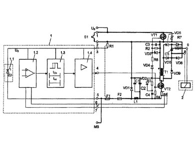
Fig. 1 a schematic circuit diagram for one example embodiment of a
circuit arrangement for actuating an electromagnetic drive system
as well as a corresponding method thereto; and
Fig. 2 the quantitative progression of the force/displacement
characteristic of
the power mechanism of the switching arrangement according to Fig. 1.
Fig. 1 shows a schematic circuit diagram of an example embodiment of a circuit
arrangement, realized here as a battery circuit breaker having a pull magnet,
its
circuit and operating principle illustrated in Fig. 1 as well as described in
greater
detail below.
The circuit arrangement comprises a regulating and control circuit 1 which in
detail
comprises a stabilizer circuit for the internal control voltage Us with ZD
1.1, a
measured value detection 1.2, a PWM circuit (pulse width modulation circuit)
with
activation time limitation t 1.3 as well as a driver circuit 1.4 for the power
switch
(VT2).
In addition, the switching arrangement comprises an electromagnetic drive
system 2.
The switching arrangement is connected to a control voltage source with an
operating voltage (UB).
The MB reference symbol indicates the negative potential (main current).
The switching arrangement moreover comprises a power button S1, a series
resistor
R1 for the current supply Us, a gate bleeder resistor R2 for the switching
transistor
VT1, a discharge resistor R3 in the snubber circuit for the power transistor
for the
self-holding circuit VT2, a gate bleeder resistor R4 for the power transistor
VT2 as
CA 03006630 2018-05-28
8
well as a standing resistor R5 for detecting the main current for the
generating of the
control variable. Further provided are a current limiting resistor R6, an
overvoltage
protector R7, a low-inductance intermediate circuit capacitor C1, an
intermediate
circuit capacitor C2 of higher storage capacity, a smoothing capacitor C3, a
capacitor
C4 of the DRC snubber circuit for the power transistor VT2, and a smoothing
capacitor 05 for the output load. The switching arrangement VD1 additionally
comprises a reverse pole diode and freewheeling diode VD1, a fast diode VD2 of
the
DRC circuit for the power transistor VT2, a gate voltage limitation VD3, a
fast rectifier
diode VD4 for the processing of the gate voltage for the switching transistor
VT1, fast
diodes for output rectification VD5, VD6, VD7 and VD8 as well as a
freewheeling
diode VD9 for the switching transistor VT1, an input choke L1 (inrush current
limitation), a thermal fuse Fl as well as an overcurrent protector F2.
An auxiliary diode connected to the transformer T1/switching transistor VT2
node on
the anode side and to the node comprised of the cathodes VD6, VD8 of the
rectifier
bridge, formed by diodes VD5, VD6, VD7, VD8, on the cathode side.
Furthermore provided are terminals 1/2, representing the power button
connections, one terminal 3 as supply input for the control current supply,
one
terminal 4 for the connection of the switching transistor VT1 activation, one
terminal
5 as negative potential of the control voltage level, terminals 6/7 as shunt
voltage
supply for the regulating circuit with measuring field detection 1.2, and
terminals 8/9
as connection for the output load 2 of the electromagnetic drive system 2.
The tEin reference symbol indicates the activation time and the ttot reference
symbol
indicates the dead time.
The functionality of the control arrangement and the inventive method will now
be
explained as below:
When activated, the battery circuit breaker reaches a mechanically locked
stable end
position. The function of safely energizing pull magnets and reliably
achieving the
mechanically fixed end position of the battery circuit breaker must be ensured
in a
CA 03006630 2018-05-28
9
voltage range of from 65V to 150V, whereby the rated control voltage amounts
to
110V.
In this application, the proposed arrangement must ensure that despite greatly
increasing power requirement ¨ as opposed to the commonly known contactors ¨
sufficient energy needs to be provided for the magnetic system at the end of
the
actuation period.
The activation process is started via the start button Si so that the
transistor VT1
in the off state is bridged and the regulating and control circuit activated
via the
series resistor R1; the control voltage processing 1.1 is symbolized by ZD. To
establish the pulse pattern, a pulse-width modulated signal at a constant base
frequency of 40 kHz is generated.
The activation time tEin is calculated such that the required pick-up time in
consideration of the permissible pull magnet operating period is maintained
under all environmental conditions, as depicted in Fig. 2.
The pull magnets 2 are designed for short-term operation; inadmissibly long
periods
of operation lead to damage. Should the permissible operating period be
exceeded
in the event of a failure, the thermal fuse Fl is activated due to the thermal
coupling
with resistor R1. Series resistor R1 and the reversible thermal fuse have the
same
basic casing design (T0220) and are mechanically connected at the thermal
contact
surfaces of the casings so as to ensure safe and defined activation in the
event of
failure. The selecting of the resistor size results in approximately thermally
equivalent
behavior to the pull magnets 2.
The transistor VT2 is activated by the regulating and control circuit 1 within
the time
tE,n of 1.6 s of the PWM circuit, a voltage generated by the rectifier bridge
of VD5 to
VD8 and smoothed by C5 corresponding to the transmission ratio of the
transformer
Ti is thereby added to the control (input) voltage UB. This arrangement
achieves the
voltage at the pull magnets being able to be brought to a value both below and
above the control voltage by varying the PWM duty cycle. Switch Si can be
CA 03006630 2018-05-28
reopened after being closed; the self-holding circuit with VT1 further powers
the
circuit by supplying the return magnetization voltage of Ti via diode VD4, the
current
limiting resistor R6 of the limiting and stabilizer circuit with VD3, R2 and
C3 to the
gate by VT1 so that it is activated. As long as the stage is clocking with
VT2, the
5 power circuit remains activated via VT1. After time tEin has elapsed, the
stage with
VT2 is deactivated, the power circuit is interrupted. After a dead time tot
has elapsed,
the switching operation can be restarted. The dead time ttot prevents the
drive
system coils from being overloaded due to improper use.
10 The internal control voltage processing 1.1 moreover ensures with its
own time stage
that stabilizer ZD is not overloaded due to improper actuation of power button
S1
(uninterrupted keying); in such a case, 1.1 is forcibly deactivated after a
predefined
period of time which is longer than the normal operating time of the device.
Capacitors Cl and C2 are provided to sufficiently decouple the inherent
resistances
of supply source UB, whereby low-inductance capacitor C1 feed in the
activation
moment of VT2 and moreover the AC portion of the intermediate circuit
capacitor C2
with the substantially higher capacity and higher internal resistance takes
over.
The choke L1 is provided for the inrush current limitation and the power
discharge
from switch Si.
The circuit is equipped with a current control; the main current is detected
in the
power circuit and fed to the measured value detection 1.2 via the shunt
resistor R5.
The measured value detection 1.2 provides the signals for the control and
regulating
circuit 1.3 which processes the pulse-width pattern according to the specific
characteristic of the electromagnetic drive system 2. A series of specific
supply
characteristics can be stored in the control and regulating circuit 1.3 which
can be
appropriately selected and thus correspond to the respective intended
application.
If there should be no connection of the output terminals 8, 9 to circuit
breaker 2 due
to an error during use, the output voltage is limited by the control and
regulating
circuit 1.3.
CA 03006630 2018-05-28
11
As is evident from Fig. 2, the force/displacement characteristic is such that
upon the
switching device 2 switching from a first switching position so corresponding
to one of
the open positions into a second switching position SEnd corresponding to the
closed
position over displacement path s, a comparatively low initial force FAnt is
initially
required which then increases to a maximum force Fmax as of a pressure point
Si up
to a maximum point s2 and, subsequent the maximum point s2, drops to a final
force
FEnd until the second switching position SEnd. The actuating force F on the
pull
magnets ZM1, ZM2 is generated according to the curve of this
force/displacement
characteristic so that the actuating force F of the force/displacement
characteristic of
the switching device 2 is adjusted.
Adapting the actuating force F to the force/displacement characteristic of the
switching device 2 ensures a less mechanically aggressive operation of the
switching device 2. In particular, excessive actuating force F is prevented
which
could lead to wear or even damage of the switching device 2 upon striking
mechanically actuated components.
In addition, adapting the actuating force F to the force/displacement
characteristic of
the switching device 2 ensures reliable switching of the switching device 2
independent of the specific control voltage Upauer available. In particular,
modifying
the control voltage UDaoer in the intermediate circuit voltage Uzi< and
adapting the
actuating force F to the force/displacement characteristic of the switching
device 2
over the entire voltage range of the control voltage Uoauer ensures that there
will be
sufficient energy to switch the switching device 2 and moreover excludes a
bouncing
of mechanically actuated components of the switching device 2.
= CA 03006630 2018-05-28
12
LIST OF REFERENCE NUMERALS
1 regulating and control circuit
1.1 - stabilizer circuit for internal control voltage Us with ZD
1.2 - measured value detection
1.3 - PWM circuit with activation time limitation t
1.4 - driver circuit for power switch (VT2)
2 electromagnetic drive system
UB - operating voltage
MB - negative potential (main current)
Si - power button
R1 - series resistor for control current supply Us
R2 - gate bleeder resistor for VT1
R3 - discharge resistor in snubber circuit of VT2
R4 - gate bleeder resistor for VT2
R5 - shunt resistor for detecting the main current to generate
the control
variable
R6 - current limiting resistor
R7 - overvoltage protector
Cl - low-inductance intermediate circuit capacitor
C2 - intermediate circuit capacitor of higher storage capacity
C3 - smoothing capacitor
C4 - capacitor of DRC snubber circuit for VT2
05 - smoothing capacitor for output load
VD1 - reverse pole diode and freewheeling diode
VD2 - fast diode of DRC circuit for VT2
VD3 - gate voltage limitation
VD4 - fast rectifier diode for processing the gate voltage for
VT1
VD5 to VD8 - fast diodes for output rectification
VD9 - freewheeling diode for Ti
VT1 - switching transistor
VT2 power transistor for self-holding circuit
CA 03006630 2018-05-28
13
Li input choke (inrush current limitation)
Fl thermal fuse
F2 overcurrent protector
Terminals: 1/2 connections for power button
3 supply input for control current supply
4 connection for activating VT1
5 negative potential (control voltage level)
6/7 shunt voltage supply for the regulating circuit
with1.2
8/9 connection for output load 2
tEin activation time
ttot dead time
actuating force
FAnf actuating force at moment of activation
Fmax actuating force at pressure point
FEnd actuating force at end of displacement path
armature path of pull magnet
So deactivation position
Si distance between deactivation position and pressure point
S2 distance between deactivation position and required maximum force
SEnd distance between deactivation and final position