Note: Descriptions are shown in the official language in which they were submitted.
METHODS OF FAST FABRICATION OF SINGLE AND MULTILAYER CIRCUIT WITH
HIGHLY CONDUCTIVE INTERCONNECTIONS WITHOUT DRILLING
FIELD
This invention is related to printed electronics, and more particularly
related to
printed electronics on porous substrates.
BACKGROUND
Printed electronics (PE) technology harnesses the existing manufacturing
capabilities of the graphics industry to produce circuitries cheaply and
quickly, and has
garnered remarkable attention in the last decade. This technology is
transforming the
electronics industry by replacing traditional costly methods of fabricating
electronic
components, devices or even systems. Increasingly, printed thin-film
transistors,
conductors, inductors and capacitors are being integrating with electronics
devices to
develop novel systems, such as thin-film energy harvesting/storage system,
smart
labels, radio frequency identification (RFID) tags and memory devices. A world
full of
flexible, wearable, even stretchable devices using printing technology is
foreseeable in
the near future.
Many demonstrations of paper electronics have been made recently; however,
existing applications of paper electronics involve the use of plastic-covered
paper
substrates, photopaper lamination of a plastic film (electronics paper
tickets) or the
gluing of electronics components, or silicon chips onto a porous substrate.
These
substrates have better chemical and physical properties than regular cellulose
paper,
1
CA 3006725 2018-05-30
but are generally more than 10 times as expensive. Fabricating a highly
conductive
circuit on a porous substrate is challenging as the porous substrate typically
has high
roughness, and cellulose fiber forms a highly porous structure that tends to
absorb
functional materials (e.g. metal nanomaterials, carbon nanotubes) instead of
leaving
them on the surface. This prevents conductive materials in the ink from
contacting each
other, making it impossible to form a highly conductive layer even after
sintering, which
leads to relatively poor performance in paper-based electronics. Additionally,
the
capillary effect of the porous substrate also causes a significant loss of
resolution when
printing with solvent-based ink.
Furthermore, the thickness of the conductor is crucial to many electronics
applications. For the same conductor, a thicker layer means a smaller sheet
resistance,
and thus the thickness usually determines the maximum current the circuits can
handle.
In the electronics industry, a standard printed circuit board with a 35 pm
thick copper
layer is adopted for most devices, loT requires a large number of RF devices
to
communicate with each other and harvest wireless energy for power. Typically,
if the
working frequency is higher than 1 MHz, then we need to consider the skin
effect, i.e.
the antenna conductor has to reach a certain thickness for optimum
performance. For
example, a copper antenna operating at 13.56 MHz has a skin effect depth of
17.7 pm
which means the thickness of the printed antenna has to be at least
approximately 17.7
pm for best performance. However, direct printing of conductive materials via
a roll-to-
roll compatible digital printing process cannot reach this level, which
greatly limits its
application in both RF devices and regular printed circuits.
2
CA 3006725 2018-05-30
,1
All of these various obstacles cause traditional printed electronics to suffer
in
performance and resolution. Thus, it is important to find a solution to these
issues to
fully utilize the low-cost, environmental-friendly properties of cellulose
paper and other
porous substrate for printed electronic technologies.
Electroless metal deposition (ELD), which relies on an autocatalytic redox
reaction to deposit various metals on a catalyst-preloaded substrate, offers a
low-cost
yet convincing solution to the thickness issue. Printed circuits fabricated
using ELD
have been demonstrated on various substrates such as PET, PI, photopaper, and
even
yarns. The thickness of the deposited metal layer can be finely tuned by the
deposition
time, but new challenges concerning adhesion and diffusion appear when
thickness is
increased. Untreated flexible substrates struggle with capturing catalyst
moieties due to
lack of binding sites, and simple physical absorption cannot prevent peeling
of the
deposited metal, especially if the thickness of the deposited metal exceeds 5
pm.
For porous substrate like cellulose paper, the loosely deposited metal
particles
tend to migrate out of the printed edge, resulting in a severe loss of
resolution. As
deposition time increases to achieve a thicker metal layer, more and more
traces in the
circuit will form connections with one another and form short circuits.
Surface
modification techniques such as UV-oxygen plasma, surface silanization,
polyelectrolyte
multilayer (PEM), and polymer grafting have been reported to enhance the
adhesion
between the electroless deposited metal layer and substrate. However, most of
these
techniques are currently far away from being a scalable cost-effective
production
method, due to their complexity and/or environmental impact and harsh
experimental
3
CA 3006725 2018-05-30
requirements. Thus, there is a need to develop a simple, low-cost and
efficient surface
modification method for all kinds of porous substrates to fabricate high
resolution thick
copper (>20 urn) paper-based electronics with strong metal-fiber bonding.
Poly (4-vinylpyridine) (P4VP) has been used for surface modification purposes
to
uptake silver ions due to its strong chelating ability with transitional metal
ions. As a
reactive monomer, 4-vinylpyridine has been used to modify substrates via in-
situ
polymerization triggered by UV and/or plasma. Such cross-linked molecules form
covalent bonds with the pretreated substrate, achieving good adhesion.
However, a low
film production rate and high equipment demands make this method not cost-
effective
and unsuitable for coating cellulose paper. P4VP molecules can be directly
coated onto
the substrate by physical absorption, but the poor adhesion will result in
serious
delamination of the electroless deposited metal.
Generally, manufacturing highly conductive circuits in a short time period
using
electroless metal deposition remains a challenge. The electroless metal
deposition
requires a relatively long time to make the circuit highly conductive because
metal
growth always happens on the surface for traditional methods. Meanwhile, it is
impossible to manufacture multilayer circuits at one time without a drill.
Such obstacles
limit the application of electroless metal deposition in the manufacturing of
printed
electronics, especially for a roll-to-roll process.
SUMMARY
4
CA 3006725 2018-05-30
The present disclosure provides a method of fabricating metal-fiber conductive
structures on a flexible, porous substrate, the method comprising the steps
of:
(i) applying a coating compound comprising poly (4-vinylpyridine) (P4VP)
and SU-8 dissolved in an organic alcohol solution to one or more surface of
the
flexible, porous substrate;
(ii) curing the porous substrate at a temperature of at least 130 C such
that
the porous substrate is coated with a layer of said coating compound;
(iii) printing a jet of a transition metal salt catalyst solution onto one
or more
printing sides of the flexible, porous substrate to deposit a transition metal
salt
catalyst onto the one or more printing sides;
(iv) submerging the substrate in an electroless metal deposition solution
to
deposit the metal on the flexible, porous substrate, wherein the deposited
metal
induces the formation of one or more three-dimensional metal-fiber conductive
structures within the flexible, porous substrate.
The step of curing the porous substrate may take place in air.
An inkjet printer may be used to print the jet of the transition metal salt
catalyst
solution onto one or more of the printing sides to deposit the transition
metal salt
catalyst onto the one or more printing sides.
The one or more printing parameters of said inkjet printer are set to achieve
a
pre-determined penetration depth of the transition metal salt catalyst
solution into the
porous substrate.
5
CA 3006725 2018-05-30
The one or more printing parameters of the inkjet printer for printing a jet
of
transition metal salt catalyst solution may be adjusted to activate a three-
dimensional
metal salt catalyst-loaded volume at a pre-specified depth below the surface
of the
porous substrate; and,
wherein a jetting waveform is used to control the volume and velocity of a
plurality of individual droplets within the jet of transition metal salt
catalyst solution.
The one or more printing parameters may include include inkjet droplet
spacing,
meniscus vacuum, printhead temperature, printhead angle and jetting voltage
The jet of transition metal salt catalyst solution printed from the inkjet
printer may
have a droplet spacing in a range from 25 pm to 50 pm.
The porous substrate may be a substrate comprising cellulose paper, porous
polyimide film, porous polyethylene terephthalate film, and textile.
The coating compound may be applied to the porous substrate by dip-coating
said porous substrate in a solution of the coating compound.
The concentration of SU-8 in a solution of the coating compound may be in a
range from about 2.5wt% to about 5 wt%.
The concentration of P4VP in a solution of the coating compound may be in a
range from 2.5 wt% to about wt 5%.
The solution of the coating compound may further comprise about 0.2 to about
1.5mg/mL of polyvinylpyrrolidone (PVP) wherein the polyvinylpyrrolidone
enhances the
6
CA 3006725 2018-05-30
ability of the coating compound to capture nanoparticles of the transition
metal salt
catalyst.
The transition metal salt catalyst in the transition metal salt catalyst
solution is
one of silver nitrate, palladium chloride and tin chloride.
The concentration of transition metal salt in the transition metal salt
catalyst
solution may be in a range from 10mM to 50mM.
The present disclosure provides a method for preparing a transition metal salt
catalyst solution containing silver nitrate, the method comprising the steps
of:
i) mixing a glycerol¨water solution of anhydrous glycerol and distilled
1.0 water at a volume ratio of 3:2;
ii) adding silver nitrate into the glycerol¨water solution to form a catalyst
solution;
iii) mixing the catalyst solution in a vortex mixer for 4 minutes to form a
silver slat solution containing 60nng/mL of dissolved silver; and
iv) degassing the silver salt solution in a vacuum chamber to remove
dissolved gases and bubbles.
The electroless metal deposition solution may be a solution comprising 14 g/L
of
CuSO4=5H20, 12 g/L of sodium hydroxide, 16 g/L of potassium sodium tartrate,
20 g/L
of EDTA.2Na, 26 mL/L of HCHO, 20 mg/L of 2,2'-dipyridyl, and 10 mg/L potassium
ferrocyanide.
7
CA 3006725 2018-05-30
The present disclosure provides an inkjet printer for carrying out the
printing a jet
of a transition metal salt catalyst solution, wherein the inkjet printer
comprises:
a mounted cartridge for loading and storing the transition metal salt catalyst
solution during the printing process, and
a piezo-electric drop-on-demand inkjet printhead for depositing the transition
metal salt catalyst solution.
The printing a jet of a transition metal-salt catalyst solution onto one or
more
sides of the coated substrate using an inkjet printer involves printing a jet
of a transition
metal-salt catalyst solution on both side of the coated substrate.
The present disclosure provides a method of fabricating multilayer metal-fiber
circuits comprising a plurality of via holes on porous substrates, the method
comprising
the steps of:
i) applying a coating compound comprising poly (4-vinylpyridine) (P4VP)
and SU-8 dissolved in an organic alcohol solution to one print surface on
each of a plurality of porous substrates;
ii) curing the plurality of porous substrates in heated air;
iii) printing a jet of a transition metal salt catalyst solution using an
inkjet
printer onto the print surface of each of the plurality of porous substrates
to deposit a transition metal salt catalyst onto the print surface;
iv) submerging each of the plurality of porous substrates in an electroless
metal deposition solution to deposit the metal on the porous substrate,
8
CA 3006725 2018-05-30
wherein the deposited metal induces the formation of one or more three-
dimensional metal-fiber conductive structures within the porous substrate;
v) with predefined aligning holes, aligning the plurality of porous
substrates
such that the print surfaces of each of the plurality of porous substrates
are facing the same direction; and
vi) performing a staking process to form a plurality of layers of the
plurality of
porous substrates.
The step of printing a jet of a transition metal salt catalyst solution may
further
comprise the step of:
printing a jet of a transition metal salt catalyst solution at a plurality of
interconnection between the plurality of layers, wherein a droplet spacing of
less than
10 microns is utilized to ensure penetration of the transition metal salt
catalyst solution
penetrates through each of the plurality of layers of the plurality of porous
substrates.
The one or more printing parameters of said inkjet printer may be set to
achieve
a pre-determined penetration depth of the transition metal salt catalyst
solution into the
plurality of porous substrates; and,
wherein a jetting waveform is used to control the volume and velocity of a
plurality of individual droplets within the jet of transition metal salt
catalyst solution.
The one or more printing parameters may include inkjet droplet spacing,
meniscus vacuum, printhead temperature, printhead angle and jetting voltage.
9
CA 3006725 2018-05-30
The jet of transition metal-salt catalyst solution printed from the inkjet
printer may
have a droplet space setting from about 2 pm to about 25 pm wherein this
spacing is
utilized for the printing of via holes.
The staking process may be one of heat staking, ultrasonic staking, cold
forming,
infrared staking and thermal punch.
A further understanding of the functional and advantageous aspects of the
present disclosure can be realized by reference to the following detailed
description and
drawings.
BRIEF DESCRIPTION OF THE DRAWINGS
Embodiments will now be described, by way of example only, with reference to
the drawings, in which:
FIG. 1 is a diagram of the fabrication process for the forming of a copper-
fiber
conductive structure on cellulose paper.
FIG. 2A is a graph of FT-IR spectra of uncoated cellulose paper, coated paper
and coated paper after thermal treatment from top to bottom with marked
characteristic
peaks;
FIG. 2B is an optical image uncoated cellulose paper ofter 3 hours of
electroless
copper deposition;
FIG. 2C is an optical image of coated and cross-linked cellulose paper after 3
hours of electroless copper deposition.
CA 3006725 2018-05-30
õ
FIG. 3 is a series scanning electron microscope (SEM) image of the surface
morphology of porous substrates after different durations of electroless
copper
deposition (ELCD). At the top right corner of each panel is an enlarged view
of the
sample.
PANEL A is a porous substrate after 0 seconds of ELCD.
PANEL B is a porous substrate after 15 seconds of ELCD.
PANEL C is a porous substrate after 15 minutes of ELCD.
PANEL D is a porous substrate after 30 minutes of ELCD.
PANEL E is a porous substrate after 1 hour of ELCD.
PANEL F is a porous substrate after 2 hours of ELCD.
PANEL G is a porous substrate after 3 hours of ELCD.
PANEL H is a porous substrate after 4 hours of ELCD.
PANEL I is a porous substrate after 5 hours of ELCD.
FIG. 4A3 is a three-dimensional AFM image of the surface morphology of a
porous substrate before electroless copper deposition.
FIG. 4B is a three-dimensional AFM image of the surface morphology of the
porous substrate of FIG. 4A after 2 hours of electroless copper deposition.
FIG. 4C is a three-dimensional AFM image of the surface morphology of the
porous substrate of FIG. 4A after 5 hours of electroless copper deposition.
FIG. 5A is a FE-SEM cross-sectional image of a sample after 5 hours of
11
CA 3006725 2018-05-30
II
,1
electroless copper deposition, showing a copper-fiber conductive structure
with
thickness of around 90 pm.
FIG. 5B is a graphical representation of the change of sheet resistance and
its
equivalent thickness in samples with different electroless copper deposition
times
ranging from 0 to 300 minutes.
FIG. 6A is a graph of the resistance change of copper-fiber conductive traces
with different electroless copper deposition times of 1 hour, 2.5 hours and 5
hours as a
function of time.
FIG. 6B is a graph of the X-ray diffraction spectra of a porous substrate
before
electroless copper deposition, freshly deposited copper traces and copper
traces stored
in air for 180 days, from top to bottom respectively.
FIG. 7A is an optically acquired image of a copper electrode array in flat
state
with initial length of Lo.
FIG. 7B is an optically acquired image of the copper electrode array of FIG.
7A in
a bent state with length of L.
FIG. 7C is an optically acquired image of the copper electrode array of FIG.
7A in
a bent state with maximum bend radii with Lmin.
FIG. 7D is a graphical representation of resistance change in copper electrode
arrays having varying electroless copper deposition times with respect to bend
rate.
FIG. 7E is a graphical representation of resistance change in copper electrode
arrays having varying electroless copper deposition times with respect to
number of
bend cycles.
12
CA 3006725 2018-05-30
FIG. 4A is an optical image of an LED powered by the copper electrode array of
FIG. 7A operating in a normal flat state.
FIG. 5B is an optical image of an LED powered by the copper electrode array of
FIG. 7A operating in a bent state
FIG. 9A is an optical image of a battery-free lighting device containing a 3 x
3
LED array on cellulose paper.
FIG. 98 is an optical image of the battery-free lighting device of FIG. 9A
operating while it is deformed to contour a cylinder which it is fixed to.
FIG. 10 is an optical image of a device which converts RF energy to electrical
energy in a bent state to illuminate all LEDs.
FIG. Ills an optical image of a bow-tie type RFID antenna with an SMA adaptor
attached to its terminal for testing.
FIG. 12 is an graphical representation of the return loss of the RFID antenna
with
respect to RF frequency.
FIG. 13 is an optical image of a double layer electrode with drill-free via
holes
fabricated using the proposed invention.
DETAILED DESCRIPTION
Various embodiments and aspects of the disclosure will be described herein
with
reference to details discussed below. The following description and drawings
are
13
CA 3006725 2018-05-30
illustrative of the disclosure and are not to be construed as limiting the
disclosure. The
drawings are not to scale. Numerous specific details are described to provide
a
thorough understanding of various embodiments of the present disclosure.
However, in
certain instances, well-known or conventional details are not described in
order to
provide a concise discussion of embodiments of the present disclosure.
As used herein, the terms "comprises" and "comprising" are to be construed as
being inclusive and open ended, and not exclusive. Specifically, when used in
the
specification and claims, the terms "comprises" and "comprising" and
variations thereof
mean the specified features, steps or components are included. These terms are
not to
be interpreted to exclude the presence of other features, steps or components.
As used herein, the terms "about" and "approximately" are meant to cover
variations that may exist in the upper and lower limits of the ranges of
values, such as
variations in properties, parameters, and dimensions.
Disclosed herein is a method for fabricating metal-fiber conductive
structures.
One of ordinary skill in the art will interpret one metal-fiber conductive
structure to be a
single conductive pathway that does not fork into more than one pathways.
In the method for fabricating metal-fiber conductive structures on a porous
substrate disclosed herein, SU-8 photoresist and Poly (4-vinylpyridine) (P4VP)
are
utilized as primary components of a coating compound. SU-8 is an epoxy-based,
negative photoresist whereby the sections of this photoresist which are
exposed to UV
become cross-linked, while the remainder of the film remains soluble and can
be
14
CA 3006725 2018-05-30
Fr
washed away during development. SU-8 is introduced to the coating compound to
act
as a bridging agent between the P4VP and the material comprising the porous
substrate. P4VP molecules are utilized for the current method as they display
a strong
uptake of catalyst metal ions used in the printing ink. P4VP molecules also
demonstrate
a strong behavior of crosslinking with epoxy. One skilled in the art will
appreciate that
the porous substrate of the present embodiment is a fibrous porous substrate
comprised of fibers but that the method of the disclosure is applicable porous
substrates
and not limited to fibrous porous substrates.
An additional benefit of applying P4VP molecules to the current process is
that
1.0 the P4VP molecules display a strong chelating ability with transitional
metal ions and as
such, there is a variety of transition metal, catalyst metal ions which may be
utilized in
the loading of catalyst metal ions in the proposed method.
Coating of Porous Substrate
In an embodiment of the current invention, the porous substrate is a cellulose
fiber substrate. Specifically, the cellulose fiber substrate of the present
embodiment is
cellulose paper. The cellulose fiber substrate may further comprise layers of
porous
polyimide film, porous polyethylene terephthalate film, and textile. The
coating
compound for application to the porous substrate is a solution of dissolved
P4VP,SU-8
in a suitable organic alcohol solvent solution. In this embodiment, the
organic alcohol
solvent solution comprises a mixture of 1,4 dioxane and 2-propanol. Referring
to the
specific composition of the coating solution, the concentration of SU-8 in the
coating
solution is in the range of 2.5 wt.%-5wt.% and the concentration of P4VP in
the coating
CA 3006725 2018-05-30
solution is 2.5wt%-5wt%. Highly reactive epoxy groups in the SU-8 tend to form
strong
bonds with cellulose fibers due to the many hydroxyl groups along the
cellulose fiber
surface, making it suitable for the current application. One skilled in the
art will
appreciate that the use of cellulose paper in the present embodiment is
exemplary and
the porous substrate of the present disclosure is in not way limited to a
cellulose fiber
substrate or to cellulose paper.
In the present embodiment of the coating solution applied to the cellulose
paper,
a small amount (0.2-1.5 mg/mL) of polyvinylpyrrolidone (PVP) is added to the
coating
solution to enhance its ability to be loaded with silver or other metallic
nanoparticles.
One of ordinary skill in the art will appreciate that the PVP that is added to
the coating
solution enhances the ability of the coating solution but that a coating
solution without
added PVP is able to produce a functional coating layer when applied to the
porous
substrate.
FIG. 1 shows the steps comprising the method for the fabrication of a high
performance, highly conductive silver ion doped circuit on cellulose paper. In
this
method, the coating solution is applied to cellulose paper 10 via a dip-
coating method
12 and is then dried in air at room temperature. The cellulose paper 10 with
coating
solution is then cured in air at 130 C, the curing process 16 involves
covalent bonding
between the cellulose paper 10 and SU-8 in the coating solution which forms a
functional coating layer 16. In addition to the covalent bonding with the
cellulose paper
10, the SU-8 in the coating solution forms covalent bonds with the pyridine
groups of
16
CA 3006725 2018-05-30
P4VP in the coating solution, leaving pyridine ligands 18 along the cellulose
fiber to
capture catalyst metal ions during the subsequent step.
In the same embodiment of the proposed method catalyst metal ions are loaded
to selected areas of a sample of cellulose paper 10 coated with the functional
coating
layer 16 by inkjet printing 20 of printing ink containing catalyst metal ions.
In a non-
limiting example, the catalyst metal ions are silver ions 22, however the
catalyst metal
ion may be one or multiple transition metal ions such that the printing ink is
a transition
metal salt catalyst. In the same non-limiting example, the printing ink is a
silver nitrate
compound; however this printing ink could be a variety of suitable transition
metal salt
catalyst compounds. For example palladium chloride and tin chloride are also
suitable
transition metal salt catalyst compounds. In this embodiment of the method,
when the
silver nitrate compound contacts the cellulose paper 10, the lone electron
pair in the
nitrogen atom of the pyridine ligands 18 will attach to the silver ions 22 to
form strong
coordinate covalent bonds. Such chemical bonding is much stronger than simple
physical absorption and helps keep the absorbed silver ions 22 adhered to the
surface.
After deposition of the printing ink onto the coated cellulose paper, the
entire
coated cellulose paper is then put into a highly alkaline, electroless metal
deposition
(ELD) bath to induce metal growth. The ELD bath of the present embodiment is
an
electroless copper deposition (ELCD) bath 24 which comprises CuSO4.5H20
(14g/L),
NaOH (12 g/L), potassium sodium tartrate (16 g/L), EDTA.2Na (20 g/L), HCHO (26
mL/L), 2,2'-dipyridyl (20 mg/L), and potassium ferrocyanide (10 mg/L).
17
CA 3006725 2018-05-30
The polyvinylpyrrolidone (PVP) in the present embodiment of the coating
solution
enhances the ability of the porous substrate to capture metal nanoparticles in
the initial
phase of the electroless copper deposition (ELCD) process. In the present
embodiment
the metal nanoparticles captured by the PVP include silver nanoparticles from
the
printing ink. The SU-8 photoresist contained in the functional coating layer
16 on the
surface of the cellulose paper 10 also acts to protect the cellulose paper 10
during an
longer duration ELCD process 24. Due to the ring-opening reaction of epoxide
groups,
the dominant bonding type will be carbon-oxygen bonds. Such bonds are highly
resistant to alkali solutions, which allows the coating solution to withstand
the highly
alkaline ELCD solution of approximately 12 pH. Due to the porous structure of
cellulose
paper 10, the printing ink will penetrate to a certain depth, forming a 3D
catalyst-loaded
area. This specific penetration of the printing ink enables copper 25 to grow
in a three-
dimensional manner, generating copper at a much faster rate than traditional
surface-
only reactions. The method generates a highly conductive metal-fiber
structure. In the
present embodiment the metal-fiber structure is a copper-fiber structure 26
because
copper is the metal used for electroless metal deposition. The copper-fiber
structure 26
enhances the flexibility of the circuits and act as anchors to firmly hold
onto the
deposited copper 25, preventing any delamination and/or peeling of the
deposited
copper 25.
In an alternative embodiment of the disclosed method, the electroless metal
deposition step uses gold, nickel or silver deposition instead of electroless
copper
deposition as used in the embodiment shown in FIG. 1.
18
CA 3006725 2018-05-30
ri
Referring to FIG. 2A to 2C, the benefits of applying the coating solution to
the
porous substrate are demonstrated through the measuring and identification of
spectra
associated with the presence of key functional groups for catalyst metal ion
bonding.
FIG. 2A compares FT-IR spectra of porous substrate samples after different
treatments.
Specifically, the different porous substrate samples are uncoated cellulose
paper,
coated cellulose paper before thermal treatment and coated cellulose paper
after
treatment. By comparing the spectra from the FT-IR results of the uncoated
cellulose
paper and the coated cellulose paper with the standard infrared transmittance
spectra
the interactions between different functional groups on the cellulose paper
and coating
can be determined. In comparing the uncoated and coated cellulose papers prior
to
thermal treatment, bands at 821, 1415, 1553, 1600 cm-lcorresponding to
pyridine
groups are present only on the spectra of coated cellulose papers. This
suggests that
the P4VP molecules have been successfully introduced and attached in the
functional
coating layer. The peaks at 915 and 1245 cm-lcorrespond to the stretching
vibration
bands of epoxide groups in SU-8, and the peaks at 1443 and 1292 cm-lmatch the
stretching frequency of C-N-C and N-C, respectively, which belong to the
pyrrolidone
groups in PVP. The presence of these peaks proves that PVP and SU-8 are
present on
the coated cellulose paper, and that these compounds can then act to improve
the
deposition process.
After thermal treatment, the stretching vibration band of epoxide groups at
1245
and 915 cm-lare weakened greatly, which suggests the occurrence of the
crosslinking
reaction. Two peaks appear at 1640 and 1658 cm-1, which are not present in
either of
19
CA 3006725 2018-05-30
the spectra of the non-heat treated samples and this can be ascribed to the
newly-
formed carbonyl groups of pyridone and the unconjugated carbon double bonds.
Additionally, the peaks for pyridine groups at 1415 and 1600 cm-lshow a slight
decrease in transmittance while the other two pyridine peaks at 821 and 1553
cm-1
have the same transmittance. This indicates that only a small amount of
pyridine ligands
reacts with epoxide groups during the thermal treatment process, resulting in
many
available pyridine groups remaining along the cellulose fibers to uptake
silver ions in the
following step. FIG. 2B shows an uncoated cellulose paper 30 after 3 hours of
ELCD
and FIG 2C shows a coated cellulose paper 32 after 3 hours of ELCD. Both
cellulose
paper samples were prepared using the same method except for the coating step
which
the cellulose paper sample 30 of FIG. 2B did not have.
Referring to FIG. 2B, the uncoated cellulose paper 30 shows a loss of
resolution
after the ELCD step due to a lack of strong bonding between silver ions and
nanoparticles and the cellulose paper 30. Highly water-soluble silver nitrate
compound
will migrate around when submerging the sample in the ELCD bath. Although
silver
nanoparticles will form at the very early stage of ELCD and the unique porous
structure
of cellulose paper will help trap silver ions to some extent, physical
absorption may not
be sufficient to fully prevent diffusion. In cases where extended ELCD is
required to
lower resistances, the severely diffused copper 34 will cover the whole area
of the
cellulose paper 30, leaving no printed feature on it.
FIG. 2C shows that the functional coating layer of the cellulose paper 32
results
in improved diffusion prevention, more complete formation of printed features
and less
CA 3006725 2018-05-30
[I
,
migration of the silver nitrate solution such that the method prints circuits
having much
higher resolution than the circuit of FIG. 2B. Upon subjecting the coated
cellulose paper
32 to an ELCD for 3 hours, there is a limited amount of catalyst diffusion and
discrete
conductive copper traces 36 with sharp edges. The hydrophobic properties of SU-
8 also
function to greatly reduce printing ink bleeding on the coated cellulose paper
32, have a
performance more similar to photopaper. The width of the copper trace 36 will
increase
by approximately 5%-8% in the first hour of ELCD and remain almost unchanged
in the
following hours. A resolution of approximately 90 pm can be achieved for 5
hours ELCD
using the proposed method. Generally the longer the duration of the ELCD
process the
better the conductivity is, but the resolution of the printed circuits will
decrease.
Surface Morphology Studies
The printed electronics on the porous substrate resulting from the proposed
method for depositing metallic ions onto a porous substrate demonstrates
altered
surface morphology during and upon completion of the ELCD process. Field
emission
scanning electron microscopy (FE-SEM) images of cellulose paper samples with
ELCD
process duration ranging from 0 to 5 hours are shown generally in FIG. 3 PANEL
A to
PANEL I, demonstrating the formation of the copper-fiber structure within the
cellulose
paper. Each cellulose paper sample initially comprises cellulose fibers 40.
FIG. 3 PANEL A shows the surface of the coated cellulose paper using the
method shown in FIG. 1 after loading of silver ions via inkjet printing,
showing a porous
structure formed by irregularly arranged cellulose fibers 40. Silver
nanoparticles 42
several nanometers in diameter can be observed along each fiber 40; these
silver
21
CA 3006725 2018-05-30
õ
nanoparticles 42 are generated from a small fraction of the printed silver
nitrate
compound undergoing self-decomposition in ambient condition. Referring to FIG.
3
PANEL B, upon 15 seconds of time elapsed since the beginning of the ELCD
process;
copper nanoparticles 44 with diameters ranging from several nanometers to
several
hundreds of nanometers have formed on the surface of each cellulose fiber 40.
FIG. 3
PANEL C shows the surface of a cellulose paper sample after 15 minutes ELCD;
most
parts of the cellulose fibers 40 have been uniformly covered by copper
nanoparticles 44
but the porosity of the cellulose paper sample remains mostly unchanged
compared to
the porosity of the cellulose paper sample shown in FIG. 3 PANEL A.
FIG. 3 PANEL D to PANEL F are FE-SEM images of the cellulose paper
samples after 0.5 hours, 1 hour and 2 hour ELCD, respectively. During this
extended
ELCD phase, copper nanoparticles 44 of larger sizes are generated at high
densities on
the cellulose fibers 40, while gaps between the cellulose fibers 40 are
gradually filled in
by the newly bonded copper. FIG. 2F shows a cellulose paper sample after 2
hours, the
coated cellulose fibers 40 have been covered by more and more copper
nanoparticles
44 and the porosity of the cellulose paper sample has greatly decreased
relative to the
porosity of the cellulose paper sample of FIG. 3 PANEL A, but all cellulose
fibers 40
remain distinct. FIG. 3 PANEL G shows a cellulose paper sample after 3 hours,
cellulose fibers 40 with distinct edges are barely seen, since most gaps have
been filled
in by deposited copper 44, indicating formation of the copper-fiber structure
46.
After formation of the copper-fiber structure 46 from the proposed method, the
most significant copper growth will occur on the surface of the cellulose
paper. Referring
22
CA 3006725 2018-05-30
to FIG. 3 PANEL G to PANEL I, corresponding to surface morphologies of 3h, 4h
and
5h ELCD cellulose paper samples respectively, it is apparent that the ELCD
process as
proposed results in a gradual smoothing of the surface as more copper is
deposited.
Referring specifically to FIG. 3 PANEL I, when 5 hours have elapsed since the
beginning of the ELCD process, no cellulose fibers are distinguishable on the
surface
and a majority of the pores in the cellulose paper have been filled in by
deposited
copper. The surface exhibits a slightly rippled morphology due to the
underlying fiber
structure.
More Studies of Surface Morphology
To achieve a better visualization of the surface morphology, an atomic force
microscope (AFM) was used to characterize the aforementioned cellulose paper
samples. FIG. 4A to FIG. 4C shows 3D images generated based on height
information
acquired from the AFM in tapping mode. FIG. 4A shows the 3D surface of a
cellulose
paper sample prior to ELCD, in a 50 pm x 50 pm window. Cellulose fibers can be
clearly identified in the image with many gaps in between. FIG. 4B and FIG. 4C
show
cellulose paper samples after 2h and 5h of ELCD respectively. Significant
improvement
of the deposited cellulose paper sample, surface morphology in comparison to
pre-
ELCD cellulose paper sample is demonstrated by a reduction in the average
surface
roughness of the substrate from a depth of 14.5 pm Ra with the 2 hours ELCD
cellulose
paper sample to a depth of 3.3 pm Ra for the 5h ELCD cellulose paper sample.
The
reduction in the surface roughness can be explained by a gradual filling in of
gaps
between cellulose fibers in the cellulose paper with copper, as deposition
progresses.
23
CA 3006725 2018-05-30
FIG. 5A shows a cross-sectional image of the cellulose paper sample 50 after
5h
of ELCD process, showing presence of copper growth 52 underneath the surface,
to a
depth of around 90 pm. This indicates that with the proposed method printing
ink
droplets can penetrate a porous substrate of cellulose 50 paper to about 90 pm
below
the surface and activate a three-dimensional catalyst-loaded volume for ELCD.
Controlling Ink Penetration Depth
In theory, the penetration depth can also be fine-tuned by adjusting the
printing
parameters. For example, a jetting waveform can be used to control the volume
and
velocity of a single droplet, and droplet spacing can be used to adjust the
printing ink
volume per unit area, factors which have a dramatic influence on the depth of
printing
ink penetration. In FIG. 5A, we can also see that most of the gaps have been
filled in
with copper 52 at the catalyst-loaded area. On top of the surface of the
cellulose paper
sample, a thin layer of copper 54 with a thickness of around 2 pm can be
observed,
covering all of the deposited area. FIG. 5A further confirms the formation of
a copper-
fiber structure.
By controlling the printing ink penetration depth, the metal deposition depth
of the
coated porous substrate can be well controlled. For the same porous substrate
and
regular ambient environment, the penetration depth is dominated by the
printing ink
properties (surface tension, viscosity, boiling point) and printing ink volume
per unit
area. There are typically two methods to control the printing ink volume per
unit area for
a piezo inkjet printer. The first is to control the jetting waveform, where a
higher peak
jetting voltage will create a larger droplet. The second way is to control the
droplet
24
CA 3006725 2018-05-30
spacing where the closer the spacing of droplets deposited on the print
surface, the
higher printing ink volume per unit area. Utilizing the structure of the
porous substrate, a
sufficiently conductive interconnection between layers can be achieved such
that the
circuit performs well without physically drilling holes.
In an additional non-limiting example, the proposed method is utilized to form
double sided circuits. In this example, the printing ink is a transition metal
salt catalyst
solution and is printed on both side of the coated porous substrate. An
interconnection
part between the layers of the porous substrate is printed using a smaller
droplet
spacing setting and higher jetting voltage for the inkjet printer settings,
which results in a
deeper penetration to a depth of more than 50% of the thickness of the porous
substrate. As both sides are printed at the interconnection part, the
transition metal salt
catalyst solution will wet through the substrate, forming a highly conductive
interconnection after completion of the electroless copper deposition process.
The change of sheet resistance with ELCD time was investigated using a four-
probe method. The sheet resistance was measured every 15 minutes during a 5-
hour
electroless copper deposition experiment. In the present embodiment cellulose
paper
was used as the porous substrate. Due to the unique porous structure of the
cellulose
paper, the thickness of the deposited copper is impossible to measure
directly, as all
cellulose paper samples have the same printing ink penetration depth. Thus, in
order to
quantify the amount of copper per unit area, we related the measured sheet
resistance
with the equivalent amount of bulk copper of a specific thickness the results
are shown
in FIG. 5B.
CA 3006725 2018-05-30
After 15 minutes of ELCD, the cellulose paper sample becomes conductive with
a very high sheet resistance of approximately2.15 x 104 Q/sq, corresponding to
the thin
and loose copper layer shown in FIG. 3C. The sheet resistance quickly
decreases
during the first hour of ELCD, which is attributed to the growth and
connection of copper
grains. As the copper grains grows larger during the first hour, they
progressively form
more contacts with other grains and increase sheet conductivity, until
finally, a dense
and uniform copper layer is formed along each fiber shown in FIG. 3 PANEL E.
The
cellulose paper sample exhibits the fastest growing rate in equivalent
thickness from 2.5
hours to 3.5 hours, which may be attributed to the rapid formation of copper-
fiber
conductive structure and the three-dimensional copper deposition mechanism
shown in
FIG. 3 PANEL to PANEL H.
In the following 1.5 hours, the equivalent thickness growth rate decreases as
most gaps have been filled with copper and thus copper growth mainly occurs on
the
surface. After 5 hours of ELCD, cellulose paper samples have a fairly low
sheet
resistance of approximately 0.00544 0/sq, which is the same as bulk copper
with a
thickness of approximately 30 pm. This value is difficult to achieve with any
other
printing method, and fulfills most thickness requirements of the printed
circuit board
industry. Thanks to the novel three-dimensional catalyst-loaded structure, we
can also
achieve a much higher average copper deposition rate (-6 pm/h) than in our
previous
ELCD papers.
Traditionally, if a piece of electroless deposited copper is thicker than 10
pm,
then the copper coating tends to delaminate or bubble up from the cellulose
paper due
26
CA 3006725 2018-05-30
to the lack of interlock between the top copper layer and the cellulose paper.
In the
disclosed method, the functional coating layer and the cellulose fiber itself
act as
chemical and physical anchors for the deposited copper to achieve strong
adhesion,
preventing any delamination or peeling of the deposited copper. An ASTM
standard
tape test was conducted to evaluate deposited copper adhesion in the freshly
prepared
samples. During the test, deposited copper conformally adhered to the surface
during
all iterations except the first, when an extremely small amount of surface
copper
particles was removed. The sheet resistance also remained unchanged throughout
all
iterations, demonstrating excellent adhesion according to the ASTM D3359
standard.
The porous structure of cellulose paper greatly enhances its deposition rate,
adhesion and flexibility; however, the drawback of such a porous structure is
that it
could be more easily oxidized in air. Hence, the relationship between
resistance and
storing time was investigated. FIG. 6A shows the resistance change of
cellulose paper
samples with 1 hour, 2.5 hours and 5 hours ELCD time over a period of 90 days.
All
cellulose paper samples were left out in open air in a room without any
temperature or
humidity control. The resistance of all cellulose paper samples increases at a
nearly
constant rate of about 0.15% per day for the first 30 days before plateauing
afterwards.
The sample with the longest ELCD time of 5h exhibits the smallest increase in
resistance after 90 days (3.5%), which may be attributed to its lower porosity
and the
generation of a thin copper top layer due to the longer duration ELCD. The
other two
cellulose paper samples show slightly higher increases, with the maximum
resistance
increase of approximately 6.5% seen in the lh ELCD sample. X-ray diffraction
(XRD)
27
CA 3006725 2018-05-30
,
was conducted to study the crystalline structure of the resultant copper
layer, as well as
the surface metal composition of fresh cellulose paper samples compared to
samples
stored for 90 days. FIG. 6B presents the XRD patterns of the coated cellulose
paper
sample, freshly made copper, and copper stored in air for 180 days. Both the
cellulose
paper sample with freshly made copper and the sample with copper stored for
180 days
were prepared with a 2 hour ELCD process. Both freshly prepared cellulose
paper
samples showed peaks at 43.46 , 50.43 and 74.25 that could be assigned to Cu
crystal plane (111), (200) and (220), respectively (JCPDS Data 04-836). For
the
cellulose paper sample stored in air for 180 days, several new weak peaks
appeared in
the spectrum. Peaks at 23.8 and 36.4 correspond to the (021) plane of
Cu(OH)2
crystal (JCPDS Data 80-0656) and (111) plane of Cu2O (JCPDS Data 05-0667)
crystal,
respectively. The other three very weak peaks at 35.5 , 38.7 and 61.5 can be
assigned to the (11-1), (111) and (11-3) planes of CuO (JCPDS Data 48-1548),
respectively, indicating a very small amount of CuO present on the surface.
From the
XRD results, we can conclude that oxidation from extended storage in open air
generates mostly Cu2O and Cu(OH)2. Furthermore, most oxidation takes place in
the
first 30 days and has limited influence on the resistance of the cellulose
paper samples
(<10%). It is also worth mentioning that the circuits could be easily
protected from
oxidization using either conformal coatings or electroless nickel deposition
for longer
shelf life.
EXAMPLES
28
CA 3006725 2018-05-30
II
The present invention can be further understood by one skilled in the art with
reference to the following examples, which the inventors technology is not
limited to in
scope. Various modifications of the present technology in addition to those
described
herein will become apparent to those skilled in the art from this description
and
accompanying figures. To achieve more reliable and predictable results from
printing
electronics on porous substrates, several methods are disclosed herein to
achieve
surface modification of the porous substrate for bonding enhancement.
Example 1
Surface modification of porous substrate
In one example of the coating, surface modification of the porous substrate
method, cellulose paper is utilized as the porous substrate. The cellulose
paper is
directly immersed into a coating solution of P4VP and SU-8 for 5 seconds. The
cellulose
paper is then slowly drawn out of the coating solution and dried in air at
room
temperature for 5 minutes. Lastly, the coated cellulose paper was placed into
an oven at
135 C for 20 minutes for in-situ cross-linking of SU-8 and P4VP molecules. One
of
ordinary skill in the art will appreciate that the above recited process is
non-limiting and
that the duration of each step may vary as long as the porous substrate after
coating is
suitable for the application of the method of the disclosure.
Example 2
Fabrication of highly conductive circuit
29
CA 3006725 2018-05-30
In one example, a highly conductive circuit is fabricated on a porous
substrate. In
this particular example, the conductive circuit is formed of a prepared,
printing ink which
is deposited via printing on the porous substrate surface. The printing ink is
prepared by
first mixing a glycerol¨water solution of anhydrous glycerol and distilled
water at a
volume ratio of 3:2. Silver nitrate is then added, followed by mixing in a
VVVR mixer for 4
minutes to form a 60mg/mL silver nitrate compound. The silver nitrate compound
is
degassed in a vacuum chamber to remove dissolved gases and bubbles. This
particular
example of the printing ink had a resulting viscosity and surface tension of
11.5 cp and
53.5 mN/m, respectively. However, one of ordinary skill in the art would
appreciate that
a variety of printing ink formulations could be used, so long as they
contained a
sufficient conductor particle concentration and so long as the resulting fluid
properties
allowed for sufficient control of droplet size and speed in the optimum
operating range
for the system's inkjet printer. In one non-limiting embodiment, a Dimatix DMP-
2800 is
used as the systems inkjet printer but one of ordinary skill in the art will
appreciate that
other inkjet printers can be used.
A 0.2 pm nylon syringe filter was used to remove undesired particles from the
printing ink. The printing ink was filled into a cartridge mounted on a 10 pL
piezo-electric
drop-on-demand (DOD) inkjet printhead. The jet of droplets from the inkjet
printer are
produced using a droplet space setting in the range of 25 pm ¨ 50 pm.
Additional
printing parameters were set as following: meniscus vacuum, 3.5 inch of H2O;
print
head temperature, 25 C; print head angle: 4.2 ; jetting voltage 25.1 V.
Printing was
conducted at room temperature. An electroless copper deposition (ELCD) bath
CA 3006725 2018-05-30
consisting of CuSO4=5H20 (14 g/L), NaOH (12 g/L), potassium sodium tartrate
(16 g/L),
EDTA.2Na (20 g/L), HCHO (26 mL/L), 2,2'-dipyridyl (20 mg/L), and potassium
ferrocyanide (10 mg/L) was prepared according to literature. Cellulose papers
with a
functional coating layer and with printed silver nitrate compound patterns
were
immersed into the bath for different periods of time.
Example 3
Fabrication of multilayer circuits without drilling
In an additional, non-limiting example, the proposed printing method is
applied to
the fabrication of multilayer circuits on multilayer substrates such that it
is unnecessary
to physically drill via holes in the multilayer substrate housing the PCB. In
this particular
embodiment, an printing ink filled cartridge is mounted on a 10 pL piezo-
electric drop-
on-demand (DOD) inkjet printhead. To achieve suitable printing results,
various printing
parameters including droplet spacing, meniscus vacuum, printhead temperature,
printhead angle and jetting voltage were all fine-tuned to suitable
parameters. In one
non-limiting procedure, the following parameters were utilized: 30 pm droplet
spacing
for regular traces, from the inkjet printer has a droplet space setting from 2
pm ¨ 25 pm
droplet spacing for via holes; a meniscus vacuum of 3.5 inch of H20; print
head
temperature of 25 C; print head angle of4.2 and jetting voltage 25.1 V.
Smaller droplet
spacing can result in higher printing ink volume per unit area, so that the
printing ink will
penetrate more into the porous substrate instead of remaining on the surface.
By
controlling the printing ink volume per unit area, the penetration depth can
be well tuned
31
CA 3006725 2018-05-30
in treated porous substrate, such that the substrate can have metal deposited
at a
desired depth.
After the printing ink is deposited on individual layers, inter-layer printing
is
completed to ensure circuit conductivity across multiple-layers of the porous
substrate.
For the printing of this conductive material at the interconnection between
layers of the
multi-layer circuits, a smaller droplet spacing (<10 microns) is utilized such
that the
printing ink is able to penetrate all through the porous substrate, connecting
the
different, multilayers after electroless copper deposition. Circuits were
printed on both
side of the coated cellulose paper including regular traces and via holes. An
ELCD bath
consisting of CuSO4-5H20 (14 g/L), NaOH (12 g/L), potassium sodium tartrate
(16 g/L),
EDTA.2Na (20 g/L), HCHO (26 mL/L), 2,2'-dipyridyl (20 mg/L), and potassium
ferrocyanide (10 mg/L). Coated cellulose papers with printed silver nitrate
compound
patterns were immersed into the ELCD bath for 3 hours. FIG. 10 shows a device
60 with
double layer electrode with drill-free via hole working properly. On the front
side, nine
LEDs in an LED array 62 with different colors (yellow, orange and red) were
mounted
on to the device 60 using 3M conductive tape. On the reverse side, a receiving
coil 64
operating at 150 kHz was fabricated, using the method proposed in this paper,
to
convert RF energy into electrical energy to power the LED array 62. The two
terminals
of the receiving coil 64 were then connected to the front side of the device
60 via two
drill-less VIAs 66. The double-layered structure can be clearly seen in FIG.
10 when the
device 60 is put under light. As a battery-free device, these LEDs will light
up using only
32
CA 3006725 2018-05-30
the energy harvested from the receiving coil 64. The fabricated device 60 is
flexible,
lightweight, and can be attached to many surfaces.
Example 4
Fabrication of RFID antennae using cellulose paper
In an additional example a paper-based RFID antenna 70 based on the popular
bow-tie design may be fabricated using the method for fabricating metal-fiber
conductive structures disclosed herein. This RFID antenna 70 demonstrates
several of
the advantages of using the proposed fabrication method. FIG. 11 shows an
image of
the antenna 70 with an SMA adaptor 72. The reflection coefficient of this
antenna 70
was measured using an Agilent Network Analyzer and the result is presented in
FIG.
12. Return loss quantifies how well energy of a selected frequency can be
coupled from
the transceiver to the antenna 70; the lower the value, the better the antenna
70. The
measured center frequency is 780 MHz with a return loss of approximately -30
db,
which is significantly lower than any result achieved by an additive printing
process. The
antenna 70 also exhibits an ultra-narrow working bandwidth of -15 MHz (775 MHz
-
790 MHz, <-15 db), making it very suitable for low-cost, energy-saving and
interference-
sensitive applications.
Example 5
Formation of Battery-less Light Source
To investigate the mechanical flexibility of the fabricated features, a linear
array
80 of five copper traces each 5 cm long and 2 mm wide spaced 1.5 mm apart was
33
CA 3006725 2018-05-30
fabricated on cellulose paper using the proposed method. The linear array 80
was
actuated between flat and bent states at a rate of 3 cm/s using a custom-made
stretching stage 84 coupled to a computer-controlled step motor. A Kethley
multimeter
was connected to the two terminals 86 of the stretching stage 84 in a four-
probe
sensing mode to measure the resistance of the sample 80.
Referring to FIG. 7A, the linear array sample 80 fabricated with the proposed
method using cellulose paper as the porous substrate is shown in a flat state.
Lo is the
initial distance of the two terminals 86; this value is divided by the actual
terminal
distance L to calculate the "bend rate" of the sample 80, i.e. FIG. 7C shows a
linear
array sample 80 with a bend rate of 50% (Lmin = 2.5 cm, LO = 5 cm). FIG. 7D
shows
the average change in resistance under different bend rates, ranging from 0%
to 50%.
When the bend rate is less than 30%, the resistance is unaffected, and even
when the
bend rate exceeds 30%, there is just a slight increase in resistance (maximum
increase
of <0.5%). These results demonstrate the excellent flexibility of the linear
array sample
80.
FIG. 7E shows the measured resistance change of linear array samples with
different ELCD times as a function of bend cycles, where for each cycle; the
linear array
sample was actuated from a bend rate of 0% to 50% at a speed of 3 cm/s. Linear
array
samples produced using the proposed method exhibit an increase in their
electrical
resistances during the first 2000 cycles, which thereafter continues to
increase but at a
slower rate. Linear array samples with a thinner copper top layer and shorter
ELCD time
will also exhibit a smaller increase in resistance. Overall, the flexible
devices exhibit
34
CA 3006725 2018-05-30
good bending durability after 10000 cycles, with a total resistance increase
of 13%, 14%
and 17% over original values for the 1 hour, 2.5 hours and 5 hours liner array
samples,
respectively.
Compared to traditional surface-only conductive features, the bending
durability
is greatly enhanced by the copper-fiber conductive structure. FIG. 8A and FIG.
8B show
how an LED light 88 powered by our copper-cellulose fiber conductive traces 80
remains operational under both normal and bent states. To demonstrate the
versatility
of the proposed technique in real world applications, a battery-free flexible
LED lighting
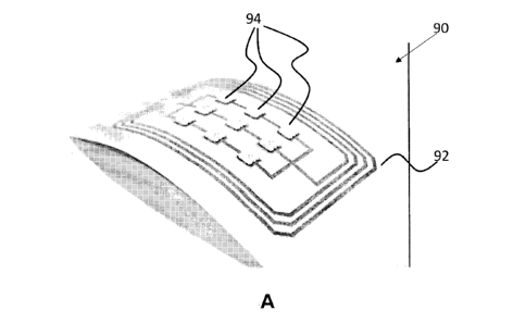
array 90 was produced. A device 90 with a receiving coil 92 operating at 150
kHz was
fabricated using the proposed method to convert RF energy into electrical
energy. Nine
LEDs 94 with different colors (red, orange, yellow) were then mounted onto the
device
90 by 3M z-axis conductive tape as shown in FIG. 9A. As a battery-free device
90,
these LEDs 94 will light up using energy converted by the receiving coil 92.
The
fabricated device 90 is flexible, lightweight, and can be attached to various
surfaces. For
example, the device 90 was attached to a glass bottle 96 and placed into a 150-
kHz 3D
electromagnetic field (EMF) generated by a custom-made device. All LEDs 92
were
illuminated and remained fully illuminated when the device 90 was moved or
bent, as
shown in FIG. 9A. In additional embodiments of this example, the LEDs may be
interchanged with other electronic components, such as sensors, displays or
actuators,
to form a variety of low-cost battery-free devices.
While the proposed method described herein are in conjunction with various
embodiments for illustrative purposes, it is not intended that the proposed
method be
CA 3006725 2018-05-30
,
limited to such embodiments. On the contrary, the proposed method described
and
illustrated herein encompass various alternatives, modifications, and
equivalents,
without departing from the embodiments, the general scope of which is defined
in the
appended claims.
Except to the extent necessary or inherent in the processes themselves, no
particular order to steps or stages of methods or processes described in this
disclosure
is intended or implied. In many cases the order of process steps may be varied
without
changing the purpose, effect, or import of the methods described.
36
CA 3006725 2018-05-30
li