Note: Descriptions are shown in the official language in which they were submitted.
CA 03006938 2018-05-30
WO 2016/092475
PCT/1B2015/059451
Description
Title of Invention:
MICRO ELECTRO-MECHANICAL STRAIN DISPLACEMENT SENSOR AND
USAGE MONITORING SYSTEM
Technical Field
The present invention relates to strain and displacement gauges. More
specifically, the
present invention relates to systems for the measurement and logging of strain
or
displacement history in a wide variety of applications, such as in mechanical
components of a fixed or a rotary wing aircraft, civil structures. machines or
vessels. It
also can work as a stand-alone or integrated sensor or recording device for
use in
variety of applications where the measured parameter can cause a displacement
such
as accelerometers and bad cells.
Background Art
In the aviation industry safety rules require that aircraft components are
constantly
monitored for fatigue as these components are subjected to a large number of
significant and prolonged mechanical stresses (or loads). Accordingly, these
components are subjected to overhauls on a regular and recurrent basis. A
number of
specific components, such as landing gears, engine pylons, etc. can
conceivably benefit
from a sensor configuration capable of recording maximum loads and therefore
providing valuable information on effects of hard landing and other
overloading
1
CA 03006938 2018-05-30
WO 2016/092475
PCT/1B2015/059451
conditions which are difficult to deduct from presently known flight recording
apparatuses.
In civil structures such as buildings, bridges, overpasses, dams, oil
reservoirs, pressure
vessels and towers knowing the history of strain experienced by the structures
can
present valuable information for assisting in predicting the maximum
stochastic loads
and the remaining working life of the structure as well as assisting in
assessing the
integrity of the structure.
Such information could also assist civil engineers conducting investigations
related to
determining the necessity of structural reinforcements in order to address the
effects of
climatic changes (i.e.: both static and dynamic loads in the form of wind,
snow, water
levels, among other loads that will be readily appreciated by the skilled
person), urban
changes (such as increasing the magnitude of transport loads on a bridge or
roadway)
and technological process changes (which can lead to increased loads due to
overhead
cranes, conveyors, etc.) on industrial buildings and other pieces of civil
infrastructure.
When structures are tested in a laboratory environment in order to monitor
strain or
displacement there are a number of limitations (including space limitations
and/or
limitations to the number of available data logging channels) that could be
overcome by
using simple and inexpensive self-contained recording gauges.
For an overall review of prior art solutions for micro-electromechanical
systems in a
variety of industrial and commercial applications, the reader is directed to
the following
academic and patent publications:
2
CA 03006938 2018-05-30
WO 2016/092475
PCT/1B2015/059451
G. Krijnen and N. Tas, "Micromechanical Actuators", MESA+ Research Institute,
Transducer Technology Laboratory, University of Twente, Enschede, The
Netherlands
A.S. Holmes, S. Lucyszyn, S. Pranonsatit and G. Hong, "Rotary RF MEMS
Switch based on the Wobble Motor Principle", Optical and Semiconductor
Devices Group, Department of Electronic & Electronic Engineering, Imperial
College London, London, UK
Z. Li and N. Tien, "Low-Cost Electroplated Vertical Comb-Drive", Berkeley
Sensor and Actuator Center, Department of Electrical and Computer
Engineering, University of California, Davis, CA
D. M. Tanner, J. A. Walraven, K. Helgesen, L. W. Irwin, F. Brown, N. F. Smith,
and N. Masters, "MEMS reliability in shock environments", Sandia National
Laboratories, Albuquerque, NM, Presented at IEEE International Reliability
Physics Symposium in San Jose, CA, April 10-13, 2000, pp. 129-138
United States Patent Publication No. 2012/0035864 to Frydenhal ¨ Determining
an Equivalent Mechanical Load
United States Patent No. 8,600,611 to Seize ¨ System and Method for
Measuring Fatigue for Mechanical Components of an Aircraft and Aircraft
Maintenance Method
Multiple Authors, "Aging Aircraft Fleets: Structural and Other Subsystem
Aspects", North Atlantic Treaty Organization, Research and Technology
Organization, Neuilly-Sur-Seine Cedex, France, presented 13-16 November
2000 in Sofia, Bulgaria
United States Patent No. 7,148,579 to Pinkerton et al. ¨ Energy Conversion
Systems Utilizing Parallel Array of Automatic Switches and Generators
S. Willis, "Next Generation Data Acquisition Technologies for Aging Aircraft",
ACRA CONTROL, Dublin, Ireland, 7th DSTO International Conference on Health
& Usage Monitoring
A. C. J. Glover, "Non-Destructive Testing Techniques for Aerospace
Applications", Inspection and Maintenance Systems Division, Olympus Australia
Pty Ltd, Victoria, Australia
United States Patent No. 7,928,343 to King et al ¨ Microcantilever Heater-
Thermometer with Integrated Temperature-Compensated Strain Sensor
United States Patent No. 7,839,028 to Pinkerton et al. ¨ Nanoelectromechanical
Systems and Methods for Making the Same
3
CA 03006938 2018-05-30
WO 2016/092475
PCT/1B2015/059451
United States Patent No. 6,744,338 to Nikitin ¨ Resonant Operation of MEMS
Switch
United States Patent No. 5,910,837 to Gimzewski ¨ Photomechanical
Transducer
United States Patent No. 5,739,425 to Binnig etal. ¨ Cantilever with
Integrated
Deflection Sensor
United States Patent Publication No. 2010/0176898 to Kihara ¨ MEMS Device
and Method for Manufacturing the Same
United States Patent Publication No. 2004/0228258 to Binnig etal. ¨ Method and
Apparatus for Reading and Array of Thermal
European Patent No. 1,226,437 to Bailer et al. ¨ Cantilever Sensors and
Transducers
T. L. Haglage, "Flight Test Evaluation of a Scratch Strain Gage", Air Force
Flight
Dynamics Laboratory (FDTR), Wright-Patterson Air Force Base, Ohio
United States Patent Publication No. 2007/0062299 to Mian etal. ¨ MEMS-
based Monitoring
United States Patent No. 5,780,727 to Gimzewski ¨ Electromechanical
Transducer
United States Patent No. 5,936,411 to Jacobsen et al. ¨ Apparatus and Method
for Measuring Strain within a Structure
United States Patent No. 6,492,820 to Adachi et al. ¨ Displacement Measuring
Device
United States Patent No. 7,412,899 to Mian etal. ¨ MEMS-based Monitoring
United States Patent No. 7,832,281 to Mian etal. ¨ MEMS-based Monitoring
United States Patent No. 6,480,792 to Prenderast ¨ Fatigue Monitoring Systems
and Methods Incorporating Neural Networks
D. M. Vidrine, "A Sequential Strain Monitor and Recorder for Use in Aircraft
Fatigue Life Prediction", Naval Postgraduate School, Monterey, California
K. L. Singh and D.V. Venkatasubramanyam,"Techniques to Generate and
Optimize the Load Spectra for an Aircraft", Structural Technologies Division,
4
CA 03006938 2018-05-30
WO 2016/092475
PCT/1B2015/059451
National Aerospace Laboratories, Bengaluru, India, 3rd International
Conference
on Integrity, Reliability and Failure, Porto/Portugal, 20-24 July 2009
L. Molent and B. Aktepe, "Review of fatigue monitoring of agile military
aircraft",
Aeronautical and Maritime Research Laboratory, Defence Science and
Technology Organisation, Victoria, Australia
S. Ariduru, "Fatigue Life Calculation by Rainflow Cycle Counting Method", The
Graduate School of Natural and Applied Sciences of Middle East Technical
University
C. Martin, "A Review of Australian and New Zealand Investigations on
Aeronautical Fatigue During the Period Between April 1995 to March 1997',
Airframes and Engines Division, Aeronautical and Maritime Research Laboratory,
Defence Science and Technology Organisation, Victoria, Australia
L. Molent, "Proposed Specifications for an Unified Strain and Flight Parameter
Based Aircraft Fatigue Usage Monitoring System", Airframes and Engines
Division, Aeronautical and Maritime Research Laboratory, Defence Science and
Technology Organisation, Victoria, Australia
D.E. Gordon, S.B. Kirschner and S.D. Manning, "Development of Fatigue and
Crack Propagation Design & Analysis Methodology in a Corrosive Environemnt
for Typoical Mechanically-Fastened Joints", General Dynamics Corporation for
Naval Development Center, Department of the Navy
United States Patent No. 7,680,630 to Schmidt ¨ Monitoring A Parameter with
Low Power Consumption for Aircraft Landing Gear-Data Logger
United States Patent Publication No. 2009/0319102 to Winterhalter et al. ¨
Flight
Recorder Having Integral Reserve Power Supply Within Form Factor of
Enclosure and Method Therefor
S. W. Arms, C. P. Townsend, D. L Churchill, S. M. Moon and N. Phan, "Energy
Harvesting Wireless Sensors for Helicopter Damage Tracking", American
Helicopter Society International Inc., proceedings of AHS International Forum
62,
HUMS III session, Phoenix, AZ, May 11th, 2006
K. Matsumoto, K. Saruwatari and Y. Suzuki, "Vibration-Powered Battery-less
Sensor Node Using MEMS Electret Generator, Department of Mechanical
Engineering, The University of Tokyo, Tokyo, Japan, TechnoDesign Co., Ltd,
Kumamoto, Japan
5
CA 03006938 2018-05-30
WO 2016/092475
PCT/1B2015/059451
DSTO International Conference on Health and Usage Monitoring, Aeronautical
and Maritime Research Laboratory, Defence Science and Technology
Organisation, Victoria, Australia, presented in Melbourne, February 19-20,
2001
J.H. Galbreath, C.P. Townsend, S.W. Mundell, M.J. Hamel, B. Esser, D. Huston,
S.W. Arms, "Civil Structure Strain Monitoring with Power-Efficient, High-Speed
Wireless Sensor Networks", MicroStrain, Inc., Williston, VT, University of
Vermont, Dept. Of Civil & Mechanical Engineering, Burlington, VT, USA,
Presented at 4th Intl Workshop on Structural Health Monitoring Stanford
University, Stanford CA, Sep 15-17, 2003
S. W. Arms, C. P. Townsend, J. H. Galbreath, S. J. DiStasi, D. Liebschutz, and
N. Phan, "Flight Testing of Wireless Sensing Networks for Rotorcraft
Structural
Health and Usage Management Systems", MicroStrain, Inc., Williston, VT, USA,
Navy/NAVAIR, Structures Division, Patuxent River, MD, 7th DSTO International
Conference on Health & Usage Monitoring
D. A. Howell and H. W. Shenton III, "System for In-Service Strain Monitoring
of
Ordinary Bridges", JOURNAL OF BRIDGE ENGINEERING ASCE,
November/December 2006
K. A. Jason and K. Surya, "A Survey of Health and Usage Monitoring System in
Contemporary Aircraft", International Journal of Engineering and Technical
Research (IJETR), ISSN: 2321-0869, Volume-1, Issue-9, November 2013
M. Neumair and W. Luber, "Structural Health Monitoring For Military Aircraft
Considering Vibration", EADS Deutschland GmbH, Munich, Germany
H. Murayama, D. Wada, and H. lgawa, "Structural Health Monitoring by Using
Fiber-Optic Distributed Strain Sensors With High Spatial Resolution", School
of
Engineering, The University of Tokyo, Tokyo, Japan, Japan Aerospace
Exploration Agency, 6-13-1 Ohsawa, Mitaka, Tokyo, 181-0015 Japan, Photonic
Sensors (2013) Vol. 3, No. 4: 355-376
S. Maley J. Plets and N. D. Phan, "US Navy Roadmap to Structural Health and
Usage Monitoring ¨ The Present and Future", Structures Division, Naval Air
Systems Command, Patuxent River, MD, American Helicopter Society
International, Inc., presented at the American Helicopter Society 63rd Annual
Forum, Virginia Beach, VA, May 1-3, 2007
United States Patent No. 5,421,204 to Svaty, Jr. ¨ Structural Monitoring
System
United States Patent No. 8,618, 928 to Weed et al. ¨ System and Methods for
Wireless Health Monitoring of a Locator Beacon which Aids the Detection and
Location of a Vehicle and/or People
6
CA 03006938 2018-05-30
WO 2016/092475
PCT/1B2015/059451
United States Patent Publication No. US 2013/0278377 to Slupsky etal. ¨
Wireless Sensor Device
S. Mahlknecht, J. Glaser and T. Herndl, "PAWIS: Towards a Power Aware
System Architecture for a SOC/SIP Wireless Sensor and Actor Node
Implementation", Institute of Computer Technology, Vienna University of
Technology, Vienna, Austria, lnfineon Technologies Austria AG, Vienna, Austria
In aerospace applications, the components used to attach the propulsion system
(Le.:
the turbo-jet engines) to the airplane as well as components such as wings,
landing
gears and critical parts of the fuselage are subjected to strict systematic
inspections.
Each overhaul requires removing the airplane from service in order to access
or remove
critical parts in order to carry out these tests.
To address these issues, Health and Usage Monitoring Systems (HUMS) have been
developed that utilize data collection and analysis techniques to help ensure
availability,
reliability and safety of vehicles, specifically commercial vehicles such as
aircraft and
trains.
The importance and benefits of structural health monitoring are well-known and
clearly
evident and include significant risk reduction, particularly in instances of
severe usage
of an aircraft, and the potential prolongation of the life of an aircraft when
the measured
usage spectrum is in fact less intense than the designed usage spectrum.
Particularly,
HUMS can significantly reduce scheduled maintenance, aborted missions and
maintenance test flights in both fixed and rotary aircraft applications (i.e.:
airplanes and
helicopters).
7
CA 03006938 2018-05-30
WO 2016/092475
PCT/1B2015/059451
Historically, fatigue prediction methodologies were an important part of an
aircraft's
safety and maintenance programs. For example, US Patent No. 8,600,611 to Seize
teaches that the frequency of the overhauls is determined in advance and an
overhaul
is carried out on expiration of each preset time period (for example every
2600 flight
cycles: takeoff - flight-landing), irrespective of the real state of fatigue
of the component.
Seize contemplates avoiding any risk that can arise when an overhaul is
undertaken too
long after a fatigue state develops and an intervention, such as a repair or a
replacement of the component, is required. Seize also provides that this
relevant time
period must be selected (either through computation or empirical analysis)
based on the
minimum period beyond which there is a risk that the component will fail, even
if this risk
remains statistically marginal.
This selected minimum period therefore corresponds to situations where the
specific
components are subjected to accidental, over-the-limit stresses; accordingly,
many
overhauls are carried out on components that could have been used without
danger for
longer since they have not been subjected to accidental stresses. Finally, in
the
absence of analysis of the real stresses to which a component has been
subjected, the
worst case scenario is always taken with respect to the possible damage that
has
occurred to the component, which can lead to overhauls that are often
conducted
prematurely.
Moreover, frequent overhauls can also introduce the additional possibility
that an error
may occur during re-assembly of the overhauled component during re-
installation.
8
CA 03006938 2018-05-30
WO 2(116/(192475
PCT/1B2015/059451
In some instances, data is collected by the inertial forces sensing unit of
the airplane to
determine whether the airplane has been subjected to exceptional stresses
(such as a
hard landing), however it can be difficult and costly to deduct an accurate
and
representative picture of the overloading of a variety of the components due
to the
sheer complexity of the overall mechanical system and the variance of the
loading
conditions, thereby resulting in a less accurate fatigue prediction.
Therefore, there is a need for a portable and self contained sensory means
capable of
recording and storing information relating to the peak stresses experienced by
a
particular component and the distribution of the stress levels historically
occurring in the
structure without adding much weight or complexity to the structure in terms
of service
and or reducing the reliability of data acquisition system or aircraft itself.
The aforementioned US Patent No. 8,600,611 to Seize provides a solution for
employing multiple sensors that each have pre-set threshold levels for
providing data
collection and analysis. Disadvantages presented by this approach relate to
the use of
multiple sensors, which can be difficult to mount at close proximity to the
point of
interest thereby introducing error in stress estimation, which can be
substantial. In
addition, the use of separate sensors (each pre--set for a specific threshold
level)
complicates the device and can lead to increased power consumption.
SU983,441 to the present inventor P. Okulov teaches a multi-contact discrete
displacement sensor which provides for automatic discrimination of threshold
levels
dividing the overall displacement into a number of levels predetermined by the
gaps
9
CA 03006938 2018-05-30
WO 2016/092475
PCT/1B2015/059451
between contacting plates. This sensor employs a stack of electrically
conductive
flexible membranes as an array of contact plates.
Another known variant of a multi-contact discrete displacement sensor that
uses an
electro-conductive flexible cantilever plates is described in association with
a system for
data acquisition from the crane loads as discussed in PhD dissertation
"Analysis of join
effects of loads from suspended cranes and snow on metal structures of roofs
of
industrial buildings", Moscow, 1985, MISI (Moscow State University of Civil
Engineering
formerly known as MISI) by the present inventor, P. Okulov.
Therefore, in one embodiment it is contemplated that the present invention can
provide
a device that can be easily attachable and detachable to the underlying
support
structure, is operable in an autonomous mode and can store information without
the
need for any external device for an extended period with the possibility of
easy retrieval
of said data through wireless means or a simple interface.
Disclosure of Invention
Technical Problem
There is an acute problem of unknown history of strain/stress in a variety of
structures
under variable loading conditions prohibiting proper evaluation of structures'
integrity
and prediction of its fatigue life.
The objective of present invention is to provide a portable, autonomous and
low power
consumption cost effective solution for an autonomous strain/displacement data
CA 03006938 2018-05-30
WO 2(116/(192475
PCT/1B2015/059451
acquisition, processing on-board and data retrieval in compressed format
allowing direct
estimate of the history of the loading of a structure and predict its
integrity and fatigue
life.
Solution to Problem
Technical Solution
The proffered embodiment includes a MEMS (Micro Electro-Mechanical System)
displacement sensor containing at least two arrays of micro or nano-size
flexible
cantilevers spaced apart in a such way so that displacement of one of the
array against
another causes sequential electrical or physical contact between adjacent
cantilevers
(utilizing Vernier effect, for instance, to avoid very small gaps between the
majority of
the adjacent cantilevers). The system and monitor has micro-processor for
processing
the data acquired, non-volatile memory for storing the processed information
and an
interface. The displacement is caused by strain of the tested structure can be
obtained
by a variety of means, preferably arranged in such a way to assure full
thermal
compensation of the device.
The present invention provides systems for the measurement and logging of
strain
history in a wide variety of applications and can work as a stand-alone or
integrated
sensor or recording device for use in variety of applications where the
measured
parameter can cause a displacement such as accelerometers and load cells.
11
CA 03006938 2018-05-30
WO 2016/092475
PCT/1B2015/059451
In at least one embodiment, the present invention provides a MEMS displacement
sensor having a plurality of deformable members and at least one driving
member
positioned in spaced relationship related to the deformable members and
providing
displacement wherein the displacement causes the deformable members to create
a
sequential contact between them wherein a predetermined spacing between the
deformable members defines the MEMS displacement sensor sensitivity to the
displacement and the state of the contacts assigned to a specific displacement
define
the output of the sensor.
In another embodiment the present invention provides a MEMS gauge such that
the
sensor has a deformable base with at least two spaced apart points of
attachment to a
test structure wherein the deformable base is connected to a substrate having
at least
two deformable members spaced apart with a predetermined gap and to a driver
member in spaced relationship to the deformable member wherein the
displacement
caused by the test structure strain and deformation of the deformable base
causes at
least one of the deformable members to contact another deformable member thus
changing the state of their contact relationship and providing an output
related to the
displacement.
In another embodiment the present invention provides a MEMS gauge for
measuring
mechanical strain or displacement in a structure having a base having a first
end, a
second end, the first end movable relative to the second end, the first end
and the
second end fixed to the structure: at least one array, each at least one array
having at
12
CA 03006938 2018-05-30
WO 2016/092475
PCT/1B2015/059451
least one cantilever, each at least one deformable member (such as, a
cantilever, for
example) having a movable, distal end and a fixed, proximal end, the fixed
proximal end
fixed to one of the first end of the base and the second end of the base, the
at least one
deformable member in electrical communication with an electrical circuit, and
a contact
fixed to the other of the first end of the base and the second end of the
base, the
contact in communication with the electric circuit such that when the first
end of the
base moves relative to the second end of the base the contact engages the
distal end of
the at least one deformable member thereby completing electrical connection
between
the engagement member and the at least one cantilever.
In another embodiment the present invention provides an autonomous predictive
system for measuring mechanical strain or displacement in a structure having a
MEMS
gauge adapted to provide an electronic signal in response to mechanical strain
or
displacement applied to the MEMS gauge, a processor in electrical
communication with
the MEMS gauge, the processor receiving the electronic signal and generating
data
output based on the electronic signal received from the MEMS gauge, an
electronic
database in electronic communication with the processor, the electronic
database
storing the data output received from the processor; and an electrical power
source for
providing electrical energy to at least one of: the processor, the MEMS gauge
and the
electronic database.
In another embodiment the present invention provides a method of manufacturing
a
MEMS displacement gauge or a strain gauge for measuring compressive and
tensile
13
CA 03006938 2018-05-30
WO 2016/092475
PCT/1B2015/059451
strain in a structure, the gauge having a base having a first end, a second
end, the first
end movable relative to the second end, the first end and the second end fixed
to the
structure, at least one array, each at least one array having at least one
deformable
member, each at least one deformable member having a movable, distal end and a
fixed, proximal end, the fixed proximal end fixed to one of the first end of
the base and
the second end of the base, the at least one deformable member in electrical
communication with an electrical circuit, and an engagement member fixed to
the other
of the first end of the base and the second end of the base, the engagement
member in
communication with the electric circuit such that when the first end of the
base moves
relative to the second end of the base the engagement member engages the
distal end
of the at least one deformable member thereby completing electrical connection
between the engagement member and the at least one deformable member.
In another embodiment the present invention provides a method of measuring
compressive and tensile strain in a structure with a MEMS gauge, the method
having
the steps of receiving an electrical output from a MEMS gauge, processing the
electrical
output to result in strain data and storing the strain data in an electronic
database. In at
least one embodiment, it is contemplated that the electrical output is output
in discrete
levels.
In another embodiment the present invention provides a MEMS displacement
sensor for
measuring mechanical strain or displacement in a structure comprising a base
having a
first longitudinally extending side, a second longitudinally extending side, a
first end
14
CA 03006938 2018-05-30
WO 2016/092475
PCT/1B2015/059451
mounted to the support structure being tested and a second end mounted to the
support
structure, the second end longitudinally translatable relative to the first
end, a first
inwardly projecting slot located in the first longitudinally extending side, a
second
inwardly projecting slot located in the second longitudinally extending side,
the first
inwardly projecting slot located across and adjacent from the second inwardly
projecting
slot, the first inwardly projecting slot and the second inwardly projecting
slot located
adjacent to one of the first end and the second end, an internal lateral slot
laterally
extending across the body from a first position inwardly adjacent the first
longitudinally
extending side to a second position inwardly adjacent the second
longitudinally
extending side, the internal lateral slot located adjacent to the other of the
first end and
the second end, a first internal longitudinally extending slot extending
between the first
inwardly projecting slot and the internal lateral slot, the first internal
longitudinally
extending slot oriented parallel to and adjacent from the first longitudinally
extending
side, the first internal longitudinally extending slot having a first inwardly
projecting
component and a second inwardly projecting component each communicating with a
longitudinally extending component; a second internal longitudinally extending
slot
extending between the second inwardly projecting slot and the internal lateral
slot, the
second internal longitudinally extending slot oriented parallel to the first
internal
longitudinally extending slot and oriented parallel to and adjacent from the
second
longitudinally extending side, the second internal longitudinally extending
slot having a
first inwardly projecting component and a second inwardly projecting component
each
communicating with a longitudinally extending component, an upwardly
projecting
central pin mounted to an upper surface of the base, a substrate fixed to an
upper
CA 03006938 2018-05-30
WO 2016/092475
PCT/1B2015/059451
surface of the base, the substrate having a central hole adapted to loosely
receive the
upwardly projecting central pin, said substrate having a central flexure
component fixed
to the substrate, the central flexure component having a central hole aligned
with the
central hole of the substrate and adapted to snugly receive the upwardly
projecting
central pin, the central flexure component having a first outer surface
adjacent the
central hole and a second outer surface adjacent the central hole, an array
having a first
plurality of deformable electro conductive micro members, each of said first
plurality of
deformable electro conductive nano or micro members transversely extending and
oriented generally perpendicular to a longitudinal axis of said body and
arranged in a
longitudinally spaced out manner; each of the first plurality of deformable
electro
conductive micro members having a fixed first end fixed to the substrate and a
movable
second end, the movable second end translatable in a generally longitudinal
direction; a
second plurality of deformable electro conductive micro members, each of the
second
plurality of deformable electro conductive micro members transversely
extending and
oriented generally perpendicular to a longitudinal axis of the body and
arranged in a
longitudinally spaced out manner; each of the second plurality of deformable
electro
conductive micro members having a fixed first end and a movable second end,
the
movable second end translatable in a generally longitudinal direction such
that when the
body is placed under tension the pin moves relative to the substrate in a
direction away
from the internal lateral slot and engages the central flexure component such
that a first
outer surface of the central flexure component engages the movable second end
of an
adjacent deformable electro conductive micro plate of one of the first
plurality of
deformable electro conductive micro members and the second plurality of
deformable
16
CA 03006938 2018-05-30
WO 2016/092475
PCT/1B2015/059451
electro conductive micro members such that when the body is placed under
compression the pin moves relative to the substrate in a direction towards the
internal
lateral slot and engages the central flexure component such that a second
outer surface
of the central flexure component engages the movable second end of an adjacent
deformable electro conductive micro plate of the other of the first plurality
of deformable
electro conductive micro members and the second plurality of deformable
electro
conductive micro members.
Advantageous Effects of invention
Advantageous Effects
The invention provides a cost effective, autonomous and extremely low power
consumption strain history monitoring system capable of recording, processing
and
storing compressed data on the entire history of meaningful stress/strain
event over
many years of operation. Its small size and simplicity of installation makes
it possible to
use the invention in variety of applications and industries helping to achieve
better
assessment of structural integrity, predict or estimate fatigue life of a
structure and
harmonize maintenance, repair and overhaul process thus reducing its costs and
allowing for improved safety.
Brief Description of Drawings
Description of Drawings
The invention is better described with reference to the drawings in which:
Figure 1 illustrates a prior art displacement sensor having metal cantilevers;
17
CA 03006938 2018-05-30
WO 2016/092475
PCT/1B2015/059451
Figure 2 illustrates a prior art displacement sensor with metal membranes and
deformable spacers positioned therebetween;
Figure 3 illustrates the basic configuration of a displacement sensor having
cantilevers
in accordance with the present invention prior to deformation of the
cantilevers;
Figure 4 illustrates the displacement sensor shown in Figure 3 after
displacement
creates sequential contacts between adjacent cantilevers;
Figure 5 illustrates an "interlaced" configuration of cantilevers allowing for
symmetrical
deformation in two directions of displacement;
Figure 6 illustrates the sensor shown in Figure 5 after deformation is applied
and
illustrates state of sequential contacts between cantilevers;
Figure 7 illustrates the basic electronic circuitry providing for change of
overall
resistance of a sensor in accordance with the present invention due to
sequential
closure of the contacts between cantilevers;
Figure 8 illustrates a circuit employing the sensor shown in Figure 7
providing voltage
output Vo;
Figure 9 illustrates the diagram of the output signal Vo related to the
displacement (a
variant with zero voltage output before the first cantilever contacts adjacent
to the drive
member makes contact);
18
CA 03006938 2018-05-30
WO 2(116/(192475
PCT/1B2015/059451
Figure 10 illustrates another embodiment of a sensor in accordance with the
present
invention having with a continual signal (no zero voltage output before the
first
cantilever adjacent to the drive member makes contact);
Figure 11 illustrates a circuit employing the sensor shown in Figure 10
providing
voltage output Vo;
Figure 12 illustrates the diagram of the output signal Vo related to the
displacement;
Figure 13 illustrates the circuit of a peak displacement recording sensor in
accordance
with the present invention having memory means consisting of non-resettable or
resettable fuses;
Figure 14 illustrates a circuit employing the sensor shown in Figure 13 where
the
output is resistance of the sensor (resistance proportional to positive peak
measured
between points A and B and resistance proportional to negative displacement
peak
measured between points C and B);
Figure 15 further illustrates a diagram of the resistance related to the peak
displacement):
Figure 16 illustrates a practical design of the MEMS sensor in accordance with
the
present invention consisting of two arrays of cantilevers and a shuttle
providing
displacement to the cantilevers causing sequential contact between them;
19
CA 03006938 2018-05-30
WO 2016/092475
PCT/1B2015/059451
Figure 17 further illustrates a simplified variant of a MEMS sensor in
accordance with
the present invention where it is positioned on a substrate and has an
integrated
resistor matrix;
Figure 18 illustrates an elevation view A of the MEMS sensor shown in Figure
17
demonstrating the position of the resistors under the cantilevers;
Figure 19 illustrates the same principle of a MEMS sensor in accordance with
the
present invention and having resistors provided in the same plane or layer as
the
cantilevers;
Figure 20 further illustrates elevation view of the sensor substrate shown in
Figure 19;
Figure 21 describes a variant of a sensor for recording peak displacement in
accordance with the present invention;
Figure 22 further illustrates elevation view A as shown in Figure 21;
Figure 23 illustrates one embodiment of the manufacturing steps (from 1 to 14)
of a
method in accordance with the present invention employing bonding of two wafer
layers
in order to provide compact configuration of the MEMS device and its attendant
circuitry;
Figure 24 illustrates a cantilever array in accordance with the present
invention and
providing mechanical memory of the cantilevers displacement before deformation
has
occurred;
CA 03006938 2018-05-30
WO 2(116/(192475
PCT/1B2015/059451
Figure 25 illustrates the same array shown in Figure 24 when several
cantilevers
maintain contact after the displacement has been applied;
Figure 26 further illustrates the effect of the cantilever length and its
affect on the
residual deflection of the cantilever;
Figure 27 illustrates a close up view of the cantilevers notches and shows a
central
hole in the base of a cantilever that facilitates memorization by the
deflection applied
wherein the shorter the cantilever free length is the more accurate "memory"
the applied
deflection;
Figure 28 illustrates the deformability and residual deformation of two
cantilevers in
accordance with the present invention having similar cross sections but having
different
lengths;
Figure 29 represents a MEMS sensor in accordance with the present invention
and
having cantilevers of different lengths thereby allowing for maintaining a
better contact
between cantilevers after removal of the displacement and thus providing for a
non-
power dependent peak displacement sensor;
Figure 30 illustrates one embodiment of a circuit implementing solution for
the MEMS
sensor shown in Figure 29, with the output being a resistance proportional to
the peak
displacement;
Figure 31 further illustrates a diagram of change in resistance after removal
of the
displacement wherein the resistance between points A and B is proportional to
the
21
CA 03006938 2018-05-30
WO 2016/092475
PCT/1B2015/059451
positive peak displacement and the resistance between points C and B is
proportional
to the negative peak displacement;
Figure 32 illustrates the general configuration of a MEMS sensor in accordance
with the
present invention encapsulated into hermetic housing (note that the inner
volume of the
sensor can be vacuum, inert gas of fluid);
Figure 33 further illustrates the elevation view A of the MEMS sensor shown in
Figure
32 where a flexible hermetic coupling for the drive member is provided in a
form of
circular shape slots surrounding the driving pin;
Figure 34 is a graphic representation of one embodiment of the peak strain
sensor in
accordance with the present invention having a battery (under blue cover) and
three
gold plated contact points for measuring resistance proportional to the peak
strain
incurred during life of the sensor;
Figure 35 illustrates the inner arrangements of a sensor in accordance with
the present
invention consisting of a base made of a material with thermal expansion
coefficient
close to the thermal expansion coefficient of the tested structure with
flexures allowing
for the relative movement of one part of the base relative to another and
where the
MEMS sensor positioned in the middle of the base for full temperature
compensation;
Figure 36 illustrates the elevation view A as shown i Figure 35 where L
denotes an
effective length of the sensor base defining the conversion of strain into
displacement;
22
CA 03006938 2018-05-30
WO 2(116/(192475
PCT/1B2015/059451
Figure 37 is yet another embodiment of a MEMS strain recording and data
processing
gauge in accordance with the present invention showing a printed circuit board
with the
MEMS displacement sensor's state detection circuitry, micro-processor or micro-
controller, memory, interface means, battery and a flexible sealant providing
for a
hermetic attachment of the sensor to the structure being tested;
Figure 38 illustrates an isometric view of a MEMS strain sensor base in
accordance
with the present invention and having nano-cantilever arrays;
Figure 39 illustrates one embodiment of the attachment of the strain sensor
base's
stand-off to the structure by glue;
Figure 40 illustrates another embodiment of the attachment of the stand-off by
a
fastener (can utilize an intermediate component glued to the surface or it can
be directly
fastened to the surface);
Figure 41 illustrates another embodiment of the attachment to a magnetic
structure
using rare earth permanent magnet incorporated into the base and in addition
shows a
coating containing high friction particles (diamond grains, for instance);
Figure 42 illustrates an overview of the strain sensor in accordance with the
present
invention and having mechanical amplification means;
Figure 43 further illustrates the rear view of the same strain sensor of
Figure 42 having
elements of the substrate having flexures provided by slots in the sensor
substrate;
23
CA 03006938 2018-05-30
WO 2016/092475
PCT/1B2015/059451
Figure 44 illustrates a cross section of the device shown in Figure 42 and
illustrating a
dome-like flexible cover necessary for mechanical protection of the MEMS
sensor and
providing hermetic seal to the MEMS sensor;
Figure 45 illustrates a diagram of the deflection applied to the cantilevers
due to
compression and tension of the structure being tested and defines the notion
of variable
size gaps between the cantilevers in order to compensate for non-linear
behavior of the
mechanical amplifier;
Figure 46 illustrates in more detail the variable gap solution in accordance
with the
present invention;
Figs. 47a) and b) illustrate the effect of thermal expansion of the sensor
substrate and
also illustrates the importance of symmetry of the positioning of the drive
member
providing the displacement;
Figure 48 illustrates in mode detail the effect of the thermal deformation of
the substrate
and the cantilevers defining an optimum ratio between the thermal deformation
properties of the materials the substrate and cantilevers are made from;
Figure 49 illustrates a variant of a shear strain sensor in accordance with
the present
invention;
Figure 50 further illustrates an embodiment of an arrangement of three linear
displacement sensors to form a rosette for assessment of all components of the
strain in
the structure being tested;
24
CA 03006938 2018-05-30
WO 2016/092475
PCT/1B2015/059451
Figure 51 illustrates a multi-layer view of the cantilever structure in
accordance with the
present invention where keeping relatively wide gaps between adjacent
cantilevers in
their plane assists achieving an overall higher resolution of the sensor;
Figure 52 is the elevation view A of Figure 51;
Figure 53 illustrates yet another arrangement of a single stack of cantilevers
in
accordance with the present invention wherein the drive member has a different
offset
from each cantilever;
Figure 54 is an elevation view A of Figure 53;
Figure 55 illustrates another configuration of stacked cantilevers in
accordance with the
present invention aligned with each other but having the drive member of
variable
shape thus providing for a sequential contact with each cantilever at
different
displacements;
Figure 56 is an elevation view A of Figure 55;
Figure 57 illustrates an arrangement of the cantilevers in a circular pattern
in
accordance with the present invention wherein the drive member experiences
angular
motion thereby causing displacement;
Figure 58 further details the deformation of the cantilevers after
experiencing said
displacement;
CA 03006938 2018-05-30
WO 2016/092475
PCT/1B2015/059451
Figure 59 illustrates another configuration of MEMS displacement sensor in
accordance
with the present invention is described wherein the relative motion
(displacement) of two
sets of cantilevers causes sequential contacts between them;
Figure 60 further illustrates the state of the contacts after the
displacement;
Figure 61 illustrates the initial state of a stack of a plurality of parallel
bridges-contacts
in accordance with the present invention;
Figure 52 illustrates the state of the contacts after the angular displacement
or torque is
applied to the ends of the stack shown in Figure 61;
Figure 63 demonstrates yet another embodiment where an array of different
length
cantilevers is compressed by a drive member and buckling of the cantilevers
causes
sequential contacts between them;
Figure 64 shows the array illustrated in Figure 63 after the buckling occurs;
Figure 65 illustrates a MEMS sensor in accordance with the present invention
that is
part of a stretchable and compressible substrate wherein the displacement is
collected
from strain but instead of causing a sequential contact of adjacent flexible
members the
sensor creates a contact condition "in parallel" where each driving member has
a
predetermined gap with a flexible member;
Figure 66 illustrates the state of the contacts illustrated in Figure 65 and
achieved after
applying compressive strain;
26
CA 03006938 2018-05-30
WO 2(116/(192475
PCT/1B2015/059451
Figure 67 illustrates the state of the contacts illustrated in Figure 65 and
achieved after
applying tensile strain;
Figure 68 illustrates a plurality of flexible bridges in accordance with the
present
invention and positioned in spaced apart configuration with 90 degrees angle
between
each adjacent flexible bridge;
Figure 69 illustrates the embodiment of the sensor where the same bridges are
wires;
Figure 70 illustrates the embodiment of the sensor where the flexible members
are
membranes;
Figure 71 illustrates the embodiment of the sensor where the flexible members
are
cantilevers clocked at a 90 degrees angle;
Figure 72 illustrates a simple configuration of the tips of cantilevers in
accordance with
the present invention;
Figure 73 illustrates cantilevers having dimples positioned symmetrically
about the
distal end of the cantilever in accordance with the present invention and
assisting more
defined contact between cantilevers and also reducing stickiness of the nano
cantilevers due to attraction forces;
Figure 74 illustrates the asymmetrical position of the dimples about the
distal end of the
cantilever in accordance with the present invention;
27
CA 03006938 2018-05-30
WO 2016/092475
PCT/1B2015/059451
Figure 75 illustrates yet another embodiment of the asymmetrical positioning
of the
dimples shown in Figure 74;
Figure 76 illustrates one embodiment of the present invention where the
cantilever has
a variable shaped cross-section;
Figure 77 illustrates a cantilever in accordance with the present invention
and having
electro conductive coatings on each side to provide for more flexible
arrangement of
electronic circuitry;
Figure 78 illustrates a cantilever with Piezo elements formed on each side of
it in
accordance with the present invention which can be utilized to generate power
necessary for the function of electronic circuitry or to force
vibration/deflection excitation
of the cantilever;
Figure 79 illustrates one embodiment of a strain sensor base in accordance
with the
present invention with Piezo-electric elements attached to parts of the
flexures to
generate additional power by harvesting it from the deformations caused by the
strain
itself;
Figure 80 illustrates one embodiment of a shuttle in accordance with the
present
invention where the Piezo-electric elements are part of the shuttle delivering
the
displacement (drive unit);
Figure 81 illustrates a cantilever in accordance with the present invention
having
variable height which can assist in achieving higher aspect ratio during MEMS
28
CA 03006938 2018-05-30
WO 2(116/(192475
PCT/1B2015/059451
manufacturing process and providing smaller gaps between the cantilevers thus
assuring better resolution of the sensor and reducing manufacturing costs;
Figure 82 illustrates one embodiment of a configuration of a MEMS displacement
sensor in accordance with the present invention where the capacitors in
circuit between
flexible members;
Figure 83 illustrates the response of the sensor shown in Figure 82 as change
in
capacitance depending on displacement;
Figure 84 illustrates a MEMS sensor in accordance with the present invention
having
resistors oriented between adjacent flexible members;
Figure 85 illustrates the response of the sensor shown in Figure 84 as change
in
overall sensor resistance;
Figure 86 illustrates an embodiment of a MEMS sensor in accordance with the
present
invention where resistors are included as an integral part of the cantilevers;
Figure 87 illustrates a response of the sensor shown in Figure 86 given that
the values
of resistors are identical;
Figure 88 illustrates an embodiment of a MEMS sensor in accordance with the
present
invention where the deformable members can have capacitors integral with them;
Figure 89 illustrates a response of the sensor shown in Figure 88;
29
CA 03006938 2018-05-30
WO 2016/092475
PCT/1B2015/059451
Figure 90 illustrates MEMS sensor with direct output from each cantilever
which can be
connected to I/0s of a circuitry, individual signal conditioning devices,
Field
Programmable Gates Array (FPGA), DIA converter, etc., Priority Encoder,
Encoder or
Complex Programmable Logic Device (CPLD) or a combination thereof;
Figure 91 illustrates a diagram of the logical states of the output from the
device shown
in Figure 90;
Figure 92 illustrates at least one embodiment of a solution comprising a self
contained
strain data acquisition and processing system for Health and Usage Monitoring
in
Aircrafts and other structures with a MEMS sensor in accordance with the
present
invention that has an analog signal output;
Figure 93 illustrates another embodiment of a solution in accordance with the
present
invention comprising a self-contained strain data acquisition and processing
system for
Health and Usage Monitoring in Aircrafts and other structures with a MEMS
sensor in
accordance with the present invention that has an digital signal output;
Figure 94 illustrates another embodiment of a solution in accordance with the
present
invention comprising a self-contained strain data acquisition and processing
system for
Health and Usage Monitoring in Aircrafts and other structures with a MEMS
sensor in
accordance with the present invention that has an digital signal output
connected to a
FGPA;
Figure 95 illustrates a number of possible placements of strain HUMS sensors
on an
aircraft;
CA 03006938 2018-05-30
WO 2(116/(192475
PCT/1B2015/059451
Figure 96 illustrates one embodiment of a strain spectrum diagram from an
element of
an aerospace structure;
Figure 97 illustrates the same signal being output of a MEMS sensor in
accordance
with the present invention and also identifies part of the signal shown in
greater
resolution in the following figures;
Figure 98 shows one of the embodiments of a MEMS sensor contacts' state
detection
circuitry employing a low power analog differentiator in accordance with the
present
invention;
Figure 99a) illustrates part of the strain measurement signal shown in Figure
97 in
greater detail;
Figure 99b) illustrates the output of the circuitry shown in Figure 98 as a
result of
differentiation of the signal produced by a MEMS sensor in accordance with the
present
invention;
Figure 100 illustrates a diagram of the partially processed signal received
from a MEMS
sensor in accordance with the present invention and compressed from real time
events
into sorted events with time stamps;
Figure 101a) illustrates the signal received from MEMS state of contacts
detection
system in accordance with the present invention;
Figure 101b) illustrates the signal shown in Figure 101a) and shaped into
short
duration wakeup pulses;
31
CA 03006938 2018-05-30
WO 2016/092475
PCT/1B2015/059451
Figure 101c) illustrates the sequence of AlD conversion process of the signal
illustrated
Figure 101b) directly following wakeup pulses;
Figure 101d) illustrates temperature reading events which can be positioned
strategically (time or event wise) to assure proper correction to the signal
received from
the MEMS sensor due to the effect of temperature;
Figure 101e) illustrates a diagram of signal conditioning based on a
temperature
reading;
Figure 101f) illustrates the frequency of time stamps initiation of which can
be linked to
a timer, pre-determined strain level events, counter of events or combination
thereof;
Figure 102 illustrates a Rainf low algorithm for data processing in accordance
with at
least one embodiment of the present invention allowing for storing only
information
relevant to estimation of peak stresses and prediction of fatigue limits (Le
the remaining
life) for the components of the aircraft being analyzed;
Figure 103 represents a table containing completely processed data per
Rainflow
algorithm; and
Figure 104 illustrates a simplified form of at least one embodiment of data
acquisition
and data processing algorithms for one embodiment of a Health and Usage
Monitoring
MEMS strain sensor in accordance with the present invention.
Best Mode for Carrying out the invention
32
CA 03006938 2018-05-30
WO 2016/092475
PCT/1B2015/059451
Best Mode
Best mode of the invention is generally illustrated by Figures 59 and 60. Two
arrays of
flexible micro or nano-scale cantilevers are in sequential contact between
adjacent
cantilevers spaced in a fashion incorporating Vernier approach. This
configuration
allows for larger gaps between the cantilevers which simplifies MEMS
fabrication while
preserving an overall high sensitivity of the sensor to a displacement. Any
suitable
means for conversion of the strain can be used to provide displacement to the
sensor,
including, but not limited to those described in Figures 35-41 or Figures 43
and 44. A
variant of the algorithm of operation of the best mode of the invention is
illustrated by
Figure 104.
Mode for the Invention
Mode for Invention
In at least one embodiment the present invention relates to a system for
monitoring and
logging displacements related to mechanical stress conditions.
As will be a readily appreciated by the skilled person, all components
discussed herein
can be manufactured of any suitable material and by any suitable manufacturing
method including those customary to nano and MEMS technological processes as
will
be readily understood by the skilled person.
These manufacturing methods and steps include but not limited to wet or dry
etching,
deep reactive ion etching, micromachining, SCREAM process, photolithography,
masking, metal deposition, SI doping, application and removal of sacrificial
layers and
33
CA 03006938 2018-05-30
WO 2016/092475
PCT/1B2015/059451
photo resists, oxidation and chemical processing, wire bonding, chemical wapor
deposition, bonding, encapsulation, thermal treatment, polycrystalline
silicone layers
deposition and removal, chemical and mechanical polishing, application of anti-
sticking
materials, treatment and techniques, sandwiching of multiple layers and
devices, etc..
In at least one embodiment of the present invention, the present invention can
provide
portable sensing means and a device for continuous monitoring, logging and
processing
of stress conditions (via displacement caused by strain) in a physical
structure, while
achieving low power consumption and adequate memory storage allowing for
monitoring over an extended period.
Another embodiment of the present invention can provide an extremely low power
consumption displacement sensor capable of easy implementation into a variety
of
applications.
Yet another embodiment of the present invention can provide a processing
algorithm
allowing for onboard analysis of the data provided by the sensing means in
order to
reduce the amount of memory needed while providing a complete picture with
respect
to the history of usage and events necessary for fatigue life prediction and
factual load
spectrum analysis.
This latter aspect can permit careful prediction of the remaining life of a
particular
monitored component and can also provide an estimation of the damage that the
component has experienced due to overloading during the use of the sensor.
Based on
this collected data and the associated knowledge that can be inferred
therefrom, it can
be possible to determine the appropriateness of the overhaul/reinforcement of
a
34
CA 03006938 2018-05-30
WO 2016/092475
PCT/1B2015/059451
component and therefore justify the necessity to replace a component only if
real,
observed damage has occurred.
In this way, the present invention can allow instrumenting an aircraft or
other structure
without interference into existing data recording instrumentation due to the
autonomous
manner that data is acquired. Alternatively, the present invention can be
employed to
enhance and assist an existing data recording system.
Moreover, constant monitoring of critical points on a structure to track and
determine a
history of stress and correlating it to the conditions causing it can allow
aircraft
manufacturers to better predict design parameters and improve the reliability
of the
systems while keeping the cost of overhauls and repairs or replacements down
to a
justified minimum.
Due to the discrete nature of the sensor output (which, as will be discussed
below, is
related to the gaps between fixed number of electrodes) it is possible to
further simplify
the circuitry and automatically implement division of the displacement range
into
predetermined threshold levels thus simplifying the computation of the desired
output as
well as watch for the state of contacts to change (i.e. from On to Off or vice
versa) in
order to initiate data acquisition only when there is a change in strain thus
dramatically
reducing power consumption of the device. It is contemplated that by varying
the gaps'
sizes any desirable sensitivity, linearity or non-linearity of the sensor can
be achieved,
as will be appreciated by the skilled person.
According to one particular embodiment of the present invention, the system
comprises
processing means for analyzing the data and storing it in non-volatile memory
making it
CA 03006938 2018-05-30
WO 2016/092475
PCT/1B2015/059451
possible to provide an output directly used for estimation of the fatigue of
the
component due to the mechanical stresses.
According to another embodiment of the present invention, each sensor
comprises
maximum/minimum (peak) stress recording means.
Yet in another embodiment of the present invention, the system comprises RF
interface
(BluetoothTM 4 or WI-Fl, for instance) for transmitting the data wirelessly
and on request
to remote means, such as for example a PC, hand-held receiver, Android device
or an
aircraft data logger.
According to at least one embodiment of the present invention, the sensors are
mechanical deformation sensors employing serially positioned flexible
electrical contact
members positioned with gaps between them and allowing for a sequential
contact of
each other by displacement of at least part of said electrical contact plate.
According to at least one embodiment of the present invention, the sensors are
of the
MEMS type comprising microelectronic and nano or micromechanical members. They
are usually manufactured using same techniques as for manufacturing of
integrated
circuits for the electronic members and using micromachining (etching, for
instance) for
the mechanical members.
The miniature size of the MEMS type sensor described herein permits easy
integration
into an aircraft or other structure and also allows for combination of several
sensors into
one package (for enhanced security using parallel data acquisition or to
create a rosette
or array of sensors for complete assessment of the strain distribution).
According to at
36
CA 03006938 2018-05-30
WO 2016/092475
PCT/1B2015/059451
least one embodiment, at least two sensors are arranged to detect the same
stress
condition at a certain point assuring that in the event of failure of one
sensor, the other
sensor can still record the stress spectrum.
The present invention can be constructed of any suitable materials. To match
the
deformation of the structure caused by temperature, the base of the sensor can
be
made of the same material as the structure being tested including metal
components
(Aluminum, steel, Inconel, Titanium, etc.), composite materials and a variety
of other
materials that will be readily apparent to the skilled person. In at least one
embodiment
the base of the sensor is made of the material with the same temperature
coefficient as
the material being tested. In addition, in some embodiments the internal
thermal sensor
can provide for correction of the sensor sensitivity at predetermined
intervals.
It is also contemplated that the invention can also provide a method for
estimating
fatigue of an aircraft component subjected to mechanical stresses using a
variety of
algorithms for data interpretation, including but not limited to a Rainfall
algorithm.
According to at least one embodiment of the present invention, a suitable
algorithm for
use in connection with the preset invention is disclosed in US Publication No.
20120035864 to Frydenhal, which teaches methods for determining an equivalent
mechanical load of a component under a dynamic mechanical loading. A first
measurement value of the mechanical load of the component is measured and
compared to a first reference value and at least one count value representing
the
number of load half-cycles of the component is updated based upon the result
of
comparing, wherein the load half-cycles correspond to a predetermined range of
37
CA 03006938 2018-05-30
WO 2016/092475
PCT/1B2015/059451
mechanical loads and occur within a time period prior to the measurement of
the first
measurement value.
According to at least one embodiment of the present invention, the data can be
organized in the memory as a table with approximately 20-50 rows indicating
mean
values related to stress fluctuation from peak to valley (or vice versa); 20-
50 columns
indicating the range of stress (from peak to valley or vice versa), two values
of absolute
maximums of tensile and compressive stress recorded and each cell of the table
containing the count of events, preferably with 32bit (or better) resolution
allowing
recording of 43 billion counts or more in each cell. The total amount of
memory for such
tables is in the range of 1.6-11 Kbytes, which allows wireless transmission of
all data
within fraction of a second. In some embodiments the table can provide
complete
information on stress spectrum and allow further calculations of the fatigue
life and
overall loading spectrum.
It is contemplated that the use of methods presented herein can allow
receiving the final
estimate of the fatigue level during routine data acquisition by any suitable
type of a
portable device operated by a user standing beside (or inside) the aircraft
within
proximity of the RF transmitter range (typically 10-50 m). It is contemplated
that
conventional wired interfaces, such as but not limited to, RS--482, One--Wire
TM or similar
interfaces can also be used as will be understood by the skilled person. Due
to data
organization as disclosed by the present invention and the small size of each
individual
sensor, a simultaneous acquisition of data from many sensors can be done
within a
very short period of time. Each sensor can have a unique identification number
and
password protection for data retrieval and changes to the sensor data
38
CA 03006938 2018-05-30
WO 2016/092475
PCT/1B2015/059451
logging/processing mission, which in some embodiments can both be accomplished
using wireless communication.
Turning to Figure 1, an illustration of a prior art electro contact
displacement sensor is
provided wherein a series of parallel cantilevers 1 are spaced apart by a
distance 62
with the help of dielectric spacers 2. In this way, when a displacement is
applied by
means of drive member 4 to an adjacent cantilever 1 a sequential contact
between
cantilevers 1 can be achieved.
Turning to Figure 2, an illustration of another prior art discrete
displacement sensor
wherein a displacement plunger 1 is received in a two part housing 2,3. An
external
gauge 4 is provided that measures the rotation of the first part of the
threaded housing 2
to the second part of the threaded housing 3 and compressive dielectric
washers 7 can
provide for adjustment of the device's sensitivity by varying gap size between
flexible
electro-conductive membranes 5.
Turning to Figure 3, at least one embodiment of the general operating
principle of the
present invention is illustrated showing an array 2 having deformable members
that are
cantilevers 4, each cantilever 4 having a movable distal end 6 and a fixed,
proximal end
8. In this embodiment, a point load is applied to the distal end 6 of an
outermost
cantilever 4 that is one of an array 2 consisting of a series of cantilevers 4
spaced apart
by a distance 6 and by means of separating members 3.
It is contemplated that the present invention employs deformable members that
can
take a wide variety of forms including, but not limited to, a plate,
cantilever, switch or
any other suitable shape that will be readily appreciated by the skilled
person.
39
CA 03006938 2018-05-30
WO 2(116/(192475
PCT/1B2015/059451
Turning to Figure 4, it can be seen that as the point load is applied to the
outermost
cantilever 4, a distal end 6 of the outermost cantilever 4 is displaced by a
displacement
A, thereby causing the distal end 6 of the outermost cantilever 4 to make
contact with
the distal end 6 of an adjacent cantilever 4. As will be appreciated by the
skilled person,
as the displacement A increases, the distal end 6 of the adjacent cantilever 4
will
eventually contact the distal end 6 of the next adjacent cantilever 4 (and so
on as the
increase of displacement A continues), as seen in Figure 4.
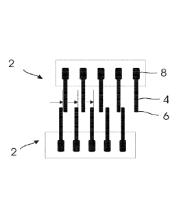
As seen in Figures 5 and 6, an analogous principle to that of Figure 3 and 4
is
illustrated, however in this embodiment two arrays 2 of cantilevers 4 (each
having a
movable distal end 6 and a fixed, proximal end 8) are presented with a contact
10
positioned therein between. In this embodiment, each array 2 of cantilevers 4
further
consists of a plurality of alternately opposing, interleaved cantilevers.
As will be appreciated by the skilled person, this arrangement permits more
cantilevers
to be placed within a given amount of surface area (due to the closely spaced,
interleaved arrangement) thereby permitting finer resolution and better
linearity with
respect to the measured displacement A, as discussed in further detail below.
As will be understood by the skilled person, provided that the contact is
movable relative
to the arrays (which are in turn fixed relative to one another) or vice versa,
this
arrangement allows the measurement of a displacement A in both directions in
cases
where the contact moves to the left relative to the arrays 2 (as seen in
Figure 6) and in
cases where the contact moves to the right relative to the arrays 2 (not
shown).
CA 03006938 2018-05-30
WO 2016/092475
PCT/1B2015/059451
As seen in Figure 6 (and in an analogous manner to the arrangement described
in
Figure 4), as displacement A increases the distal end of the outermost
cantilever makes
contact with the distal end of an adjacent cantilever (which in this
arrangement is
located across from the outermost cantilever). As the displacement A further
increases,
the distal end of the adjacent cantilever will eventually contact the distal
end of the next
adjacent cantilever (located across from the adjacent cantilever and on the
same side of
outermost cantilever) and so on as the increase of displacement A continues,
as seen in
Figure 6.
Turning to Figures 7 and 8, at least one embodiment of the present invention
is
illustrated wherein a contact 10 is disposed between a first array 2 of
cantilevers 4 and
a second array 2 of cantilevers 4. Each cantilever 4 has a movable, distal end
6 and a
fixed, proximal end 8 and is spaced apart from an adjacent cantilever 4 by a
distance O.
Further, A resistor 12 having an electrical resistance 0 is placed between
each pair of
adjacent cantilevers 4.
Contact 10 is electrically connected to an electric circuit (at point B), and
each cantilever
4 of each array 2 are electrically connected to a circuit (at points A and C).
In this way a circuit is provided, as seen in Figure 8, wherein a supply
voltage Võ is
measured at point A, an output voltage Vo is measured at point B and point C
is
grounded. Therefore, the voltage measured between point B (Vo) and point C
(V=0) is
an output voltage V0. as will readily be appreciated by the skilled person.
As can be seen in Figure 9, displacement A of the contact 10 relative to the
arrays 2 of
cantilevers can be plotted against the output voltage V, measured between
points B and
41
CA 03006938 2018-05-30
WO 2016/092475
PCT/1B2015/059451
C. In this particular embodiment, negative displacement can be plotted as the
contact
moves to the left relative to the arrays 2 and positive displacement can be
plotted as
the contact 10 moves to the right relative to the arrays 2, although other
arrangements
are certainly contemplated as will be understood by the skilled person.
5 In the present embodiment, at the initial position also shown in Figure
7, there is zero
output voltage (Le.: V, = 0) when the contact is in the initial position
(displacement A
0), as the contact does not make contact with a cantilever in either array
thereby
opening the circuit between points B and C.
As contact 10 moves to the left relative to the arrays 2 by a distance
corresponding to
1.0 distance 5, contact 10 makes electrical contact with the distal end 6
of the left outermost
cantilever 4 thereby completing the circuit. In this position the output
voltage is
measurable. As the contact 10 continues to move to the left relative to the
arrays 2 by
an additional distance O. the distal end 6 of the left outermost cantilever 4
makes
contact with the distal end 6 of an adjacent cantilever 4. As this occurs, a
single resistor
1.5 12 is removed (shorted) from the circuit and the total measured
resistance across points
B and C is reduced by the resistance 0 of resistor 12. Therefore, in
accordance with
Ohm's law, the output voltage Vo measured across points B to C is reduced by a
stepwise amount VA, as seen in Figure 9.
Turning to Figures 10 and 11, another embodiment of the present invention is
illustrated wherein contact 10 is disposed between a first array 2 of
cantilevers 4 and a
second array 2 of cantilevers 4. Each cantilever 4 has a movable, distal end 4
and a
fixed, proximal end 8 and is spaced apart from an adjacent cantilever 4 by a
distance O.
42
CA 03006938 2018-05-30
WO 2016/092475
PCT/1B2015/059451
Further, A resistor 12 having an electrical resistance D. is placed between
each pair of
adjacent cantilevers 4.
Contact 10 is electrically connected loan electric circuit (at point B), and
each cantilever
4 of each array 2 are electrically connected to a circuit (at points A and C).
In this
embodiment, an additional resistor 14 is placed in electrical communication
between
contact 10 and each of the arrays 2 such that the circuit is complete when
contact 10 is
in the initial position between each of the arrays 2.
In this way a circuit is provided, as seen in Figure 11, wherein a voltage V,
is measured
at point A, an output voltage V, is measured at point B and point C is
grounded.
Therefore, the voltage measured between point B (V0) and point C (V=0) is an
output
voltage V0. as will readily be appreciated by the skilled person.
As can be seen in Figure 12, displacement A of the contact 10 relative to the
arrays 2 of
cantilevers can be plotted against the output voltage V, measured between
points B and
C. In this particular embodiment, negative displacement can be plotted as the
contact
10 moves to the left relative to the arrays 2 and positive displacement can be
plotted as
the contact 10 moves to the right relative to the arrays 2, although other
arrangements
are certainly contemplated as will be understood by the skilled person.
In the present embodiment, at the initial position also shown in Figure 10,
there is an
initial output voltage (i.e.: V, = Vi) when the contact is in the initial
position
(displacement z = 0), as in this embodiment contact 10 (at point B) is in
electrical
communication with both points A and C through additional resistor 14.
43
CA 03006938 2018-05-30
WO 2(116/(192475
PCT/1B2015/059451
As contact 10 moves to the left relative to the arrays 2 by a distance
corresponding to
distance 5, contact 10 makes electrical contact with the distal end 6 of the
left outermost
cantilever 4 thereby completing the circuit. In this position the output
voltage is
measurable. As the contact 10 continues to move to the left relative to the
arrays 2 by
an additional distance O. the distal end 6 of the left outermost cantilever 4
makes
contact with the distal end 6 of an adjacent cantilever 4. As this occurs, a
single resistor
12 is removed (shorted) from the circuit and the total measured resistance
across points
B and C is reduced by the resistance 0 of resistor 12. Therefore, in
accordance with
Ohm's law, the output voltage Võ measured across points B to C is reduced by a
1.0 stepwise amount V,A, as seen in Figure 12.
Turning to Figures 13 and 14, another embodiment of the present invention is
illustrated wherein contact 10 is disposed between a first array 2 of
cantilevers 4 and a
second array 2 of cantilevers 4. Each cantilever 4 has a movable, distal end 4
and a
fixed, proximal end 8 and is spaced apart from an adjacent cantilever 4 by a
distance O.
A resistor 12 having an electrical resistance 0 is placed between each pair of
adjacent
cantilevers 4. Further, in each array 2, a fuse 16 is placed in electrical
contact between
the proximal end 8 of each cantilever 4 and ground.
Contact 10 is electrically connected to an electric circuit (at point Vs), and
each
cantilever 4 of each array 2 are electrically connected to a circuit (at
points A and C).
Further, the entire circuit is connected to point B and ground as seen in
Figure 13.
In this way a circuit is provided, as seen in Figure 14, wherein points Vc, A,
B and C are
connected to the circuit. Further, the entire circuit is also grounded.
Therefore, the
44
CA 03006938 2018-05-30
WO 2(116/(192475
PCT/1B2015/059451
output resistance R, measured between point Vc and ground, as will readily be
appreciated by the skilled person.
As can be seen in Figure 15, maximum (peak) displacement A of the contact 10
relative
to the arrays 2 of cantilevers can be plotted against the output resistance R,
measured
between points Vc and ground. In this particular embodiment, negative peak
displacement can be plotted as the contact 10 moves to the left relative to
the arrays 2
while fuses 16 are sequentially burned and positive peak displacement can be
plotted
as the contact 10 moves to the right relative to the arrays 2 while fuses 16
are
sequentially burned, although other arrangements are certainly contemplated as
will be
understood by the skilled person.
In the present embodiment, at the initial position also shown in Figures 13
and 15,
there is no output resistance (i.e.: Rõ = 0) when the contact is in the
initial position
(displacement A --- 0), as in this embodiment contact 10 (at point B) is not
in electrical
communication with either points A and C and the electrical circuit is not
completed. The
circuit per Figure 13 employs two diodes 17 which assist measuring the
resistance
between points A-B and points C-B without interference on the readings from
the
adjacent array of resistor-fuse matrix.
As contact 10 moves to the left relative to the arrays 2 by a distance
corresponding to
distance 5, contact 10 makes electrical contact with the distal end 6 of the
left outermost
cantilever 4 thereby completing the circuit. However, and as discussed above,
as the
electrical connection is completed between left outermost cantilever 4 and
contact 10
the first fuse 16 connected to the ground is receiving voltage Vc. Thus, as
proximal end
CA 03006938 2018-05-30
WO 2(116/(192475
PCT/1B2015/059451
8 of cantilever 4 is in electrical connection with ground through .fuse 16 the
.fuse is blown
(burned). After reaching this contact state the output resistance proportional
to the peak
displacement is measurable. As the contact 10 continues to move to the left
relative to
the arrays 2 by an additional distance 5, the distal end 6 of the left
outermost cantilever
4 makes contact with the distal end 6 of an adjacent cantilever 4. As this
occurs, a
single resistor 12 previously shorted by fuse 16 is added to the circuit and
the total
measured resistance across points B and C is increased by the resistance U of
resistor
12. Therefore, in accordance with Ohm's law, the output resistance Ro measured
across
points B to C is increased by a stepwise amount RA, as seen in Figure 15.
As contact 10 moves to the right relative to the arrays 2 by a distance
corresponding to
distance 5, contact 10 makes electrical contact with the distal end 6 of the
right
outermost cantilever 4 thereby completing the circuit. As discussed above, as
the
electrical connection is completed between right outermost cantilever 4 and
contact 10
the first fuse (on the right from the contact 10) 16 connected to the ground
is receiving
voltage Vc. Thus, as proximal end 8 of cantilever 4 is in electrical
connection with
ground through fuse 16 the fuse is blown (burned). After reaching this contact
state the
output resistance proportional to the peak displacement is measurable. As the
contact
10 continues to move to the left relative to the arrays 2 by an additional
distance 5, the
distal end 6 of the left outermost cantilever 4 makes contact with the distal
end 6 of an
adjacent cantilever 4. As this occurs, a single resistor 12 previously shorted
by fuse 16
is added to the circuit and the total measured resistance across points B and
C is
increased by the resistance O. of resistor 12. Therefore, in accordance with
Ohm's law,
46
CA 03006938 2018-05-30
WO 2016/092475
PCT/1B2015/059451
the output resistance 1:10 measured across points B to C is increased by a
stepwise
amount RA, as seen in Figure 15.
Turning to Figure 16, a plan view of one embodiment of the array substrate
arrangement for use in connection with a strain gauge in accordance with the
present
invention is illustrated. In this embodiment, the contact 10 is a central
flexure (or shuttle)
component having a central, displacement driver hole 14. Central flexure
component is
fixed to an underlying substrate by way of anchored pads 180, as will be
discussed in
further detail below. An array 2 of opposing, interleaved cantilevers 4 is
oriented on
each side of contact 10. Each cantilever 4 has a movable, distal end 6 and a
fixed,
proximal end 8. The fixed, proximal end 8 is fixed to the underlying array
substrate by
anchored pads. A stopper 22 is positioned at each end of the array substrate.
Stoppers
22 are provided that abut the outer end of each array 2.
Turning to Figures 17 and 18, a simplified diagram of one embodiment of an
array
substrate arrangement for use in connection with a strain gauge in accordance
with the
present invention is illustrated. A contact 10 that is a central flexure
component having a
central, displacement driver hole 14 fixed to an underlying substrate 20. An
array 2 of
opposing, interleaved cantilevers 4 is oriented on each side of contact 10.
Each
cantilever 4 has a movable, distal end 6 and a fixed, proximal end 8. Adjacent
cantilevers 4 are connected electrical communication with one another by way
of a
network of resistors 12 that are arranged in a series relationship with one
another.
Further, an additional resistor 15 is provided to connect the contact 10 to
the adjacent
cantilevers 4 in electric communication.
47
CA 03006938 2018-05-30
WO 2(116/(192475
PCT/1B2015/059451
With reference to Figure 18, a side view of the array substrate arrangement of
Figure
17 is depicted. As can be seen, a conductive layer 30 is provided between the
cantilever 4 and the underlying substrate 20 in order to anchor the fixed,
proximal end 8
of the cantilever 4 to the underlying substrate 20. Conductive layer 30 can be
constructed of any suitable material having the electrical and thermal
properties
required by the particular application. In this particular instance the layer
30 is used to
create an electric circuit with integrated resistors 12.
Turning to Figures 19 and 20, a simplified diagram of another embodiment of an
array
substrate arrangement for use in connection with a strain gauge in accordance
with the
present invention is illustrated. A contact 10 that is a central flexure
(shuttle) 19
component having a central, displacement driver hole 14 fixed to an underlying
substrate 20. An array 2 of opposing, interleaved cantilevers 4 is oriented on
each side
of contact 10. Each cantilever 4 has a movable, distal end 6 and a fixed,
proximal end 8.
In this embodiment, cantilevers 4 are connected in electrical communication by
way of a
network of resistors 12 that are arranged in a branched relationship with one
another.
Contact pads 23 are provided to electrically connect cantilevers 4 and
resistors 12 to an
overall electrical circuit. Further, additional resistors 15 are provided to
connect the
contact 10 to the adjacent cantilevers 4 in electric communication.
With reference to Figure 20, a side view of the array substrate arrangement of
Figure
19 is depicted. As can be seen, a conductive layer 30 is provided between the
cantilever 4 and the underlying substrate 20 in order to anchor the fixed,
proximal end 8
of the cantilever 4 to the underlying substrate 20.
48
CA 03006938 2018-05-30
WO 2016/092475
PCT/1B2015/059451
Turning to Figures 21 and 22, a simplified diagram of another embodiment of an
array
substrate arrangement for use in connection with a strain gauge in accordance
with the
present invention is illustrated. A contact 10 that is a central flexure
(shuttle) 19
component having a central, displacement driver hole 14 is fixed to an
underlying
substrate 20. An array 2 of opposing, interleaved cantilevers 4 is oriented on
each side
of contact 10. Each cantilever 4 has a movable, distal end 6 and a fixed,
proximal end 8.
In this embodiment, cantilevers 4 are connected in electrical communication by
way of a
network of resistors 12 that are arranged in a series relationship with one
another. In
this embodiment, a series of fuses 16 is provided to connect the proximal end
8 of each
cantilever 4 to ground. Contact pads 23 are provided to electrically connect
cantilevers
4 and resistors 12 to an overall electrical circuit. Further, diodes 18 are
provided to
connect the contact pad 17 to the adjacent cantilevers 4 in electrical
communication.
Contact pads 23 may be used to wire the sensor to the external circuitry.
With reference to Figure 20, a side view of the array substrate arrangement of
Figure
19 is depicted. As can be seen, a conductive layer 30 is provided between the
cantilever 4 and the underlying substrate 20 in order to anchor the fixed,
proximal end 8
of the cantilever 4 to the underlying substrate 20.
Turning to Figure 23, the manufacturing steps of MBAS sensor per one of the
variants
are depicted, namely:
Step -I illustrates a Silicon wafer prior to undergoing any processing steps;
Step 2 illustrates masking the silicon wafer;
49
CA 03006938 2018-05-30
WO 2(116/(192475
PCT/1B2015/059451
Step 3 illustrates forming a layer of silicon oxide as electric isolator;
Step 4 illustrates the removal of the masking as per step 2;
Step 5 illustrates forming the conductive layer and masking it with a pre-
determined pattern;
Step 6 illustrates forming an electric circuit on the conductive layer;
Step 7 illustrates removal of masking per step 5;
Step 8 illustrates the bonding of the silicon wafer to a substrate (for
example, a
silicon wafer);
Step 9 illustrates masking of the top silicon wafer to create a pattern of
1.0 cantilevers;
Step 10 illustrates removal of masking per step 9;
Step 11 illustrates forming cantilevers on the top silicon wafer;
Step 12 illustrates the removal of the masking per step 9;
Step 13 illustrates the removal of the sacrificial layer (silicon oxide, for
instance)
formed in steps 3 and 4; and
Step 14 shows metallization of cantilevers by conductive layer deposition or
Silicon doping and forming the sensor circuitry.
CA 03006938 2018-05-30
WO 2(116/(192475
PCT/1B2015/059451
Turning to Figure 24, one embodiment of an aspect of the present invention is
illustrated wherein an array 2 of cantilevers 4 is provided that consists of a
series of
spaced apart, opposing, interleaved cantilevers 4. Each cantilever 4 has a
movable,
distal end 6 and a fixed, proximal end 8. A hinge 5 is positioned between the
proximal
end 8 and the distal end 6. In this embodiment, hinge 5 of cantilever 4 is
located closer
to the proximal end 8, however other embodiments are also contemplated.
With reference to Figure 25, it is contemplated that hinges 5 provide for
plastic
deformation of the material that cantilevers 4 are made from. In a preferred
embodiment, the cantilevers 4 are made from metals with fairly well defined
plastic
deformation region in their strain-stress curve (see, for example Figure 28
below).
These metals include, but not limited to such materials as gold and aluminum.
To
further facilitate plastic deformation responsible for mechanical memory of
the cantilever
4 deflection after the source of deformation is released, the hinge 5 can have
a notch
(not shown) or a recess providing for stress concentration and/or reduction of
the cross
section where the elastic deformations occur.
Initially, the cantilevers are spaced apart by gaps 25, however when a
displacement
force is applied to the distal end 6 of an outer cantilever 4 the distal end 6
makes
contact 27 with the distal end 6 of an adjacent cantilever 4, as illustrated
in Figure 25.
Turning to Figures 26 and 27, in at least one embodiment it is contemplated
that for a
given deflection 6 the shorter the length of the cantilever 4 the larger the
final (i.e.:
memorized) deflection 6' can be. In other embodiments, it is contemplated that
the
deformable element can be a bridge, membrane or any other suitable stricture
rather
51
CA 03006938 2018-05-30
WO 2(116/(192475
PCT/1B2015/059451
than a cantilever in order achieve the same effect. It is also contemplated
that the
deformable material can be formed of any suitable material provided that the
selected
material has the desired properties of remembering its shape once deformed.
This effect is further illustrated in Figure 28, from which it is apparent for
the skilled
person that there is a combination of relative lengths of cantilevers 4
wherein they will
maintain mechanical contact (and electric) after the displacement is removed
thus
providing for a simple means for memorizing the peak deformation or strain
resulting in
such deformation.
At least one embodiment of a device incorporating these principles on a MEMS
scale is
illustrated in Figure 29. In this embodiment, wherein two arrays of opposing
interleaved
cantilevers 4 are arranged in a spaced apart arrangement on either side of a
contact 10
that is a central flexure (shuttle) 19 component having a central,
displacement driver
hole 14 that is fixed to an underlying substrate 20. In this embodiment it is
contemplated
that each cantilever 4 is in electrical connection with the adjacent
cantilevers and further
include a hinge 5 positioned between distal end 6 to fixed end 8.
More specifically, in this embodiment a resistor 12 is placed in electrical
connection
between adjacent cantilevers. Further, in this embodiment each cantilever 4
within a
given array 2 has different lengths (measured from distal ends 6 to fixed ends
8) that
increase sequentially as one moves toward the outer edges of the substrate 20
(that is,
away from contact 10).
52
CA 03006938 2018-05-30
WO 2016/092475
PCT/1B2015/059451
Turning to Figure 30, one embodiment of an electrical block diagram suitable
for use in
connection with the device illustrated in Figure 29 is illustrated.
Therefore, and as can be seen in Figure 31 Output Resistance R can be plotted
against Displacement A for the device illustrated in Figure 29 such that for
each
increase in displacement 5 a corresponding increase in the Output Resistance R
can be
measured across the circuit (which in fact corresponds to the differential
Resistance
measured between points A and B). As will be understood by the skilled person,
this
corresponds to the device being placed in a condition of tension.
On the other hand, for each decrease in displacement 5 that occurs a
corresponding
increase in the Output Resistance R can also be measured across the circuit
(which in
fact corresponds to the differential Resistance measured between points C and
B). As
will be understood by the skilled person, this corresponds to the device being
placed in
a condition of compression.
Figure 32 illustrates a self-contained displacement sensor incorporating an
array of
MBAS cantilevers 4 for detecting deformation of the center of the shuttle 10.
The
sensor substrate 20 with device layer comprising the cantilevers 4, shuttle 10
and
electronic circuitry has a deformable part 64 formed by etching circular slots
from
opposite sides of the substrate and providing for hermetic seal of the inner
volume of
the sensor while allowing for deformation of the shuttle 10 via pin (not
shown) in contact
with pocket 200 in the drive member (see also Figure 33). The housing is
bonded to the
substrate using conventional techniques, for instance epoxy 60. To achieve
better
compensation for thermal deformation, the substrate has recesses 201
positioned close
53
CA 03006938 2018-05-30
WO 2016/092475
PCT/1B2015/059451
to the vertical symmetry line (perpendicular to direction of displacement) for
attachment
of the sensor to the device producing the displacement to be measured. The
elevation
per Figure 32 is shown in Figure 33. Thermal compensation technique will be
described in more detail further down the description.
With reference to Figure 34, scale illustrated wherein a representative peak
strain
sensor in accordance with the present invention is displayed alongside a
traditional ruler
(with millimeter resolution) indicating the scale at which certain embodiments
of the
present invention can operate. The sensor has plastic housing 120 with
hermetically
sealed gold plated contact pads 121 (which represent test points A, B and C
per Figure
14) and a battery's (not shown) cover 122.
Turning to Figures 35 and 36, a plan and elevation view of one embodiment of a
MEMS sensor is illustrated. In this embodiment, a substrate 20 supporting an
electric
circuit 1 and MEMS device layer with arrays 2 of deformable members (not
shown)
having a central displacement hole 14, is mounted to an underlying mounting
body or
base 40. Mounting body 40 has a first end 42 and a second end 44 that are
fixed to an
underlying support structure 46.
The mounting body 40 has positions 123 for placement of standoffs 124 which
are
shown in more detail further down in Figure 37. These positions 123 belong to
one part
of the body 40, thus any deformation of the support structure 46 does not
cause any
stress on the elements on internal circuitry which are attached to it and
therefore
provides for free deformation of the mounting body 40.
54
CA 03006938 2018-05-30
WO 2016/092475
PCT/1B2015/059451
It is contemplated that in some embodiments of the present invention first end
42 is
movable relative to second end 44 such that mounting body 40 can contract or
expand
in concert with the expansion or contraction of the underlying support
structure 46. This
can be achieved in a number of ways. For example, a number of slots can be
provided
in mounting body 40 that permit first end 42 to move relative to second end
44, however
other arrangements are also contemplated including hinges or pivoting joints
that can
be incorporated in mounting body such that first end 42 can move relative to
second
end 44, thereby transferring the expansion or contraction of the underlying
support
structure 46 to the deformable members of the MEMS sensor, thereby permitting
measurement of strain and displacement in the underlying support structure 46.
As seen in Figures 35 and 36, in this embodiment mounting body 40 has a pair
of
opposed, inwardly projecting slots 50, a pair of opposed, internal
longitudinal slots 52
that longitudinally extend across body 40. Each internal longitudinal slot 52
has a first
laterally extending slot 54, longitudinally extending slot 56 and a second
laterally
extending slot 58. Body 40 also has an internal, laterally extending internal
slot 60.
The substrate 20 is connected to the body 40 preferably at its centerline
using bounding
compound 125 during the assembly of the sensor. Again, mounting substrate this
way
provides for its free expansion or contraction due to temperature fluctuations
without
imposing any stress on the mounting body 40.
As will be discussed in further detail below, this arrangement allows for the
body 40, to
be able to deform (and subsequently measure via displacement of the MEMS
sensory
means) both compression and tension.
CA 03006938 2018-05-30
WO 2(116/(192475
PCT/1B2015/059451
Figure 37 illustrates the elevation of at least one embodiment of a self-
contained tvlEMS
Health & Usage Monitoring System( HUMS). In this embodiment, base 40 has two
posts
42 and 44 spaced apart and attached to the surface 46 of test structure (for
instance an
aluminum alloy part of an aircraft) by means of glue. The strain in the test
structure is
converted into displacement A over the active length Ls of the base, i.e.,
121.c*Ls
wherein c is the strain.
Standoffs 124 hold the printed circuit board 126 with all electronic circuitry
needed for
operation of the HUMS, namely, but not limited to: battery 127, CPU, MCU, FPGA
or
CPLD 128, F-Ram or other type of memory 129, interface and/or wireless
transceiver
(not shown) and connector 130. All devices are mounted inside housing 131
which is
hermetically sealed. During mounting process, the housing 131 is glued to the
surface
46 as well as sealing deformable compound (silicone sealant, for instance) 132
applied
previously (during gauge manufacturing process) or during installation of the
gauge is
provided to ensure that interior volume of the sensor is not affected by
moisture, dust or
debris.
Further, detail A is shown to clarify on possible installation techniques
described in
more detail in the following Figures 39-41.
Figure 38 illustrates the construction of the base 40 and positioning of the
MEMS
sensor 133 relative to it. Flexible hinges are formed in the base by providing
slots in its
structure (by laser cut or water jet cut technique, for example) as discussed
above in
relation to construction of base 40 and possible ways of providing its
deformability
described previously in Figure 34, therefore providing for ability of one part
of the base
56
CA 03006938 2018-05-30
WO 2(116/(192475
PCT/1B2015/059451
to move against another part without much stress imposed on the attachment
layer
(glue, in this instance) between the posts and the surface. A central pin 22
is provided
that can move relative to the sensor in order to transmits the relative
displacement A of
the support structure to the MEMS sensor.
A housing 131 and elastic seal 132 are glued to the structure, preferably in
one step
with gluing the posts 42 and 44. Connector 130 provides for a wired interface
(such as,
for example, RS-485). As mentioned, the printed circuit board 126 is connected
to the
base 40 via standoffs 124 in a such way that the attachment does not
compromise the
freedom of two parts of the base to move one relative to another, i.e. all of
them are
connected to one part of the base (see attachment points indicated in Figure
38). The
circuitry in its generic configuration contains power supply (battery, power
harvesting
means, super capacitor, etc.), processing means (microcontroller, for
instance), memory
means, sensor signal conditioning means and interface means (wired, wireless,
optical
fibre, ultrasound, light emitting and/or receiving, etc.). The wireless module
can be part
of the housing 131 and have its antenna incorporated into the printed circuit
board 125
(as an example) as well as it can be a stand alone unit with its own power
supply or
connected to an onboard power. The stand alone wireless transceiver can be
connected to the gauge via cable using connector 130 and the two module can
share
communication protocol as well as power supply or power harvesting means.
The nodes structure can also be employed to collect data from a number of
strain
gauges and transmit data via a dedicated transceiver or wired interface
(parallel, or
serial, One-Wire, for instance).
57
CA 03006938 2018-05-30
WO 2(116/(192475
PCT/1B2015/059451
A variety of attachment options are presented in the following illustrations:
In Figure 39
the sensor is attached to the underlying support structure 46 by gluing
directly to the
surface of the tested structure using suitable bonding compound 136. In Figure
40 the
sensor is attached to the underlying support structure 46 by a fastener 138
connected to
a pad 137 attached to the tested structure or, alternatively, directly to the
support
structure 46. In Figure 41 the sensor is attached to the underlying support
structure by
frictional force produced, for example, by a magnet 139. In embodiments where
frictional attachment is employed a special coating 140 can be applied to the
interface
between the sensor base and tested structure surface to increase the friction
therebetween, such as an abrasive coating, for instance (diamond, aluminum
oxide,
etc.). In addition, the base 40 or any integral part of the gauge can be used
to facilitate
magnetic flux (preferably create a closed loop) and reduce the size of the
magnet's 139
while achieving sufficient attraction force necessary for providing adequate
friction. It is
contemplated that these variants are examples only, and accordingly one
skilled in the
art can employ a variety of permanent and removable methods of attachment
including
snap means, positioning means, and affixing means, as will be readily
understood by
the skilled person.
It is contemplated that a wide variety of mechanical amplification means can
be
employed in connection with present invention including sloped beams 141
(single or
arranged as parallelogram mechanisms) with hinges or flexural hinges 142, as
shown in
for example in Figure 42. In some embodiments strain is transformed into
relative
displacement of pads 143 that can be amplified via sloped simple or
parallelogram
beams and the resulting displacement is acting to create contact state in two
arrays 2 of
CA 03006938 2018-05-30
WO 2016/092475
PCT/1B2015/059451
cantilevers 4. As also discussed above, the substrate has pre-cut slots 52,
54, 56, 58
and 60 to allow relative movement of the two parts 143 of substrate 40 (in
this particular
case the substrate 20 previously mentioned is acting as body 40) while
maintaining its
physical integrity.
Turning to Figure 43, the back view of the sensor is illustrated in more
detail.
Turning to Figure 44, details of the elevation A-A per Figure 42 are
illustrated wherein
the tested structure surface 46 and substrate 40 are connected to one another
using
bond 145 (adhesive glue) and an elastic layer 146 can provide a hermetic seal
of the
sensor in its part affected by slots. The elastic layer 146 can also be made
in a form of
protective film which has openings allowing for bond 145 to be present active
only at
areas of pads 143 attached to the base (substrate) 40. In this case the
substrate 40 acts
as the deformable base of the sensor and device layer 147 has mechanical
amplification means (beams 141 with pads 143 and shuttle 148), cantilevers 4
and other
components necessary for operation of the sensor. The cover 150 is deformable
to
provide freedom of movement for the parts of substrate and also can be adapted
in
order to provide a hermetic seal. The inner volume 151 of the sensor can be
filled with
fluid (inert gas, dielectric fluid, for instance) or contain vacuum. The cover
150 has a
bond 152 connecting it to the device layer 147 or substrate 40 or both.
As most mechanical amplification mechanisms are non-linear, compensation for
that
effect can be done assuring variable size gaps between cantilevers as
described in
Figures 45 and 46. In general, the case of sloped beam gives the following
relation
between the displacement of the sensor driver A and the strain E of the tested
structure:
59
CA 03006938 2018-05-30
WO 2016/092475
PCT/1B2015/059451
A = a - ao =(((U2)2 a02) - (L/2 - e*U2)2)" - ao,
where "a" is the height of the sloped beam after deformation of the tested
structure and
"a0" is the height of the sloped beam at initial state.
The principle of thermal compensation of the MEMS sensor is illustrated in
Figure 47 a)
(sensor geometry before thermal expansion) and Figure 47 b) (sensor geometry
after
thermal expansion). The deformation in vertical direction (axis Y) does not
affect
sensor's sensitivity, however the deformation in horizontal direction (axis X)
changes the
distance between cantilevers 4 and the thickness of the cantilevers tips, thus
introducing an error.
1.0 Taking a close look at the state of two adjacent cantilevers 4 as shown
in Figure 48 we
can define that the distance of first cantilever X1 and the second cantilever
X2 after
thermal expansion (here, thermal expansion is used only for illustration, it
is understood
that thermal contraction will also take place under sensor usage conditions)
will
become:
X1' = X1 + Ks*AT* X1= X1*(1 +Ks* AT);
X2' = X2 + Ks*AT* X2= X2*(1 +Ks* AT),
Where:
Ks is coefficient of thermal expansion of the substrate the cantilevers 4 are
anchored to;
CA 03006938 2018-05-30
WO 2016/092475
PCT/1B2015/059451
AT = T2 -T1 is temperature difference between the final and initial state of
the sensor,
9C.
Accordingly, the thermal deformation of the cantilevers in direction of axis X
itself will
be:
ti' = t1 + K*AT* tl= ti*(1 +K*AT);
= t2 + K*AT* t2= t2*(1+K*AT),
where "t" is the initial thickness of the cantilever in direction X;
K is coefficient of thermal expansion of the material of cantilevers.
Therefore, the final size of the gap 50' will be:
O.' = X2'4272-X1'41'12
501 =X2*(1+ Ks* AT)- t2*(1 -1-K* AT)/2- X1*(1+Ks* AT)- ti*(1+K* AT)
or, if 1:142=t
50' =X2*(1+Ks* AT) - X-1*(1+Ks* AT) - t*(1+K* AT)
Thus, the condition of unchanged gap (full thermal stability) will require the
following
equation to be observed:
508 - 50
Where 50 = X2-X1-t
61
CA 03006938 2018-05-30
WO 2016/092475
PCT/1B2015/059451
X2*(1+Ks* AT) - Xi*(1+Ks* AT) - t*(1+K* AT) . X2 - X1 - t;
X2* Ks* AT - Xi *Ks* AT . t*K* AT;
X2* Ks - Xi *Ks . t*K;
K/Ks. (X2 - Xi)/t.
S If b . (X2 - Xi) represents the spacing between cantilevers and t is the
thickness of the
cantilever, i.e. b = t + 60, the ratio K/Ks is close to 1. For example, if t =
20pm and gap
60 . 2 pm, the ratio
K/Ks . (20 + 2)/20 . 1.1.
In many embodiments the substrate and cantilevers are made of silicon crystal
(SIC) or
polycrystalline silicon (polysilicon). If the substrate is made of SIC where
coefficient of
thermal expansion Ks.2.6 ppm/QC and the device layer is composed of
polycrystalline
silicon where coefficient of thermal expansion K.2.8 ppm/QC, the desired ratio
K/Ks
2.8/2.6 . 1.08 - 1.1 is approximately achieved and gives the nearly perfect
thermally
compensated MEMS sensor for the example of sensor geometry used here above.
1.5 Another combination of materials can be Alumina for the substrate (Ks .
5.4 ppm/QC)
and Ruthenium for cantilevers (K. 6.4 ppm/QC), therefore K/Ks . 6.4/5.4 . 1.18
and so
on.
In addition to the embodiments disclosed herein, alternative approaches that
will be
readily appreciated by the skilled person are also contemplated for use in
connection
62
CA 03006938 2018-05-30
WO 2016/092475
PCT/1B2015/059451
with the present invention including thermal compensation techniques by
design,
thermal compensation by acquiring temperature readings at continuously or at
pre-
determined time intervals and electronic compensation for the signal read from
the
sensor output are provided for in the present invention as will be described
in more
detail later.
It is contemplated that there are numerous variants of use of the present MEMS
sensor.
For instance, a sensor configured to measure shear deformation is shown in
Figure 49
where the shear strain is transformed into displacement activating contact
state
between cantilevers 4 and drive member 10.
Another embodiment of the MEMS strain sensor is a rosette as shown in Figure
50.
The rosette allows for simultaneous measurement of all planar vector
components of
the strain (stress) at given point of measurement not unlike in a conventional
strain
gauge rosette. In tis particular arrangement the sensor has a base 40 with
flexural
pivoting points allowing for its deformation and attachments 160 and 161
wherein the
attachment 161 in the center of the base 40 is not always necessary as the
strain
vectors can be assessed through measurement of the relative displacement of
only
three points (160).
A variety of arrangements of flexible contact members vs. drive member is
presented in
Figures 51 to 56. Several layers of cantilevers' arrays can be positioned with
an offset
relative to each other thus increasing overall sensitivity of the device while
providing a
manufacturability wise possible gap 60 between adjacent cantilevers 4.
Alternatively, an
array of single cantilevers positioned in several layers with the offset can
be used as
63
CA 03006938 2018-05-30
WO 2016/092475
PCT/1B2015/059451
shown in Figures 53 to 54. Yet another arrangement can include multi-layer
cantilevers
positioned without offset between them but having drive member 10 with step-
like
profile to achieve sequential contact at different displacements of the drive
member 10
as shown in Figures 55 to 56.
It will be appreciated that a combination of the above techniques and
arrangements can
be used by one skilled in art and also employing a variety of techniques
available for
manufacturing of MEMS devices.
The MEMS sensor can be arranged to receive an angular movement of the drive
member as shown in Figure 57 to 58.
Yet another approach is to provide MEMS sensor where spacing between
cantilevers
can vary on one side of the array compared to another side thus providing for
sequential
contacts during movement of one array against another (Figures 59 to 60)
utilizing so-
called Vernier effect and thus providing for higher resolution of the sensor
while keeping
the majority of the gaps between cantilevers large enough to use lower aspect
ratio
MEMS etching techniques. The same approach can also be used in providing a
sensor
capable of encoding the displacement into a sequence of binary output signal
not unlike
rotary encoders work.
Sequential contact between deformable members made, for instance in a form of
stacked bridges being bent as shown in Figure 61 to 62 can also be achieved.
Still, the sequential contact can be achieved by collapsing or buckling of
cantilevers
having different length as shown in Figures 63 to 64.
64
CA 03006938 2018-05-30
WO 2016/092475
PCT/1B2015/059451
Sequential contact state between drive members and deformable contacts (or
vice
versa) can be achieved given an example shown in Figures 65 to 67. In this
particular
case the MEMS sensor contains an array of individual drive members and
deformable
members arranged in a such way that the size of the gaps between them in each
member of an array is different. Thus the contact state is achieved at each
individual
member of an array at different strain level of the substrate. Given the
length Lo
between the anchoring point of a drive member and the center of the deformable
member is the same (it may vary) during compression of the substrate attached
to a test
structure (Figure 66) and during extension of the substrate (Figure 67) the
contact
state corresponding to a particular level of strain can be detected via
acquisition of the
contact state of each individual member (drive member and deformable member.
In this
particular instance, either the drive member or deformable member or both can
have
electro--conductive surface on each side facing each other and independent
from
another member of the array.
It will be appreciated by one skilled in the art that significant scaling down
of the MEMS
sensors described is achievable. Going to nano--scale systems the complete
sensor
(including its variants for detecting/recording volume strain caused
displacement (3D) or
multi-axial acceleration forces, pressure, loads, etc.) the volume as small as
1mm3 can
contain up to 4 arrays on deformable members providing resolution of 1000
displacement states and higher. Even with today's technology this task is
achievable
without much modification to the manufacturing process. Going further, such
systems
as microphones and sound amplifiers driven by signal digitized directly by
sensor into
discrete but undetectable for ear levels can lead to systems eliminating
amplifier at all,
CA 03006938 2018-05-30
WO 2(116/(192475
PCT/1B2015/059451
thus providing for conversion of a displacement into much amplified signal
directly,
using digital technology.
The term "state of the contacts" in present invention should be represented in
a broad
fashion, i.e. it can be manifested as an electrical contact providing lower
resistance
(Ohmic) circuit between electro-conductive layers, using electron-tunneling
effect,
change in vibration state of a particular deformable member of an array, its
thermal
conductivity or temperature state, etc. Thus any combination of the
technologies
applicable for detection of the state of the contact can be applied per
present invention.
"Driving member" shall also be broadly interpreted as a rigid or flexible
member that
may comprise a plurality of cantilevers or other means as illustrated in
Figures 59-60,
for instance.
As sensor sensitivity is of major importance, a variety of calibration
techniques can be
envisioned. For instance a removable attachment of the MEMS strain sensor to a
calibration beam (not unlike calibration of the batches of strain gauges is
done) by
removable adhesive, frozen water or another substance, fasteners, friction,
etc. Thermal
sensitivity calibration can be also done and a specific correction parameter
entered into
MEMS sensor data acquisition system to ensure temperature correction.
Turning to acceleration sensitivity of the MEMS sensor the following example
illustrates
that an array of cantilevers 600pm long with cross-section of 20 by 20 pm and
gap
between cantilevers of 2 pm can withstand acceleration in the plane of the
array of up to
5000G without causing closure of any gap between cantilevers.
66
CA 03006938 2018-05-30
WO 2016/092475
PCT/1B2015/059451
In this particular instance, given the cantilever is formed from
polycrystalline silicon with
density of 2.33 g/cm2 or 2.33 x10⁻⁶ pg/pm3 the mass of its free length is
m = 20*20*600*2.33 x104 . 0.56 pg = 0.56*10=6 kg.
The distributed load on cantilever beam from acceleration will be:
S W = m*a*(G.9.82kg/m2)/L, where a is acceleration, L is the free length of
the cantilever
beam.
Therefore the load will be:
W = a(G)*0.56*10-9[kg]*9.82[kg/m2]/600*104 = a(G)*9.15*10'6 [N/m]
Maximum deflection of the free end of the cantilever beam is:
Ac = W*L4/8/E/I,
where E is modulus of elasticity (Young's modulus) of polycrystalline silicon
and I is
moment of inertia of the cantilever beam cross-section (note, that the
practical thickness
of the polycrystalline silicon layer is typically much less than 20 pm, we use
this
example as explanatory only).
1.5 E . 155 GPa or 0.155 Nipm2
I . 20*203/12 = 13333 pm4 = 1.33*10-20 m2 (for the rectangular cross-section)
Ac = a(G)*( 9.15*104 [N])*0.00064[m1/8/155*109[P01.33*10 Im41
67
CA 03006938 2018-05-30
WO 2016/092475
PCT/1B2015/059451
a(G)*7.19*1 011[m] = a(G)*7.19*10-5[pm].
Thus, at acceleration a(G) . 5000 the total deflection of a single cantilever
will be
Ac= 5000*7.19*10-6. 0.35 pm, which is less than a gap of 2 pm.
Turning now to stress condition of the cantilever beam at acceleration of
5000G (which
S is higher than current specification from EUROCAE - European Organisation
for Civil
Aviation Equipment - requires for an airplane flight recorder to withstand the
acceleration of 3400G), the maximum bending stress at anchored part of the
cantilever
beam is:
a.W*1.2/2/1*h/2,
where h . 20 pm . 20*10=6m is the height of the cantilever cross-section.
Thus:
,
O . 5000*9.15*10-6 *0.0006[m]2/2/1.33*1020
" imzi*20*10"6[m1/2 = 6.19*106 [Pa] .
. 6.19 MPa,
which is much less than the fracture strength of the polysilicon
conservatively estimated
1.5 at 1.5 GPa.
For reduction of shock effect of the strain on sensor base 40 the best
methodology is to
reduce its size so that stress on attachments of the sensor to a test
structure can be
68
CA 03006938 2018-05-30
WO 2(116/(192475
PCT/1B2015/059451
reduced. To that extend it is desirable to further scale down the MEMS sensor
and
provide better sensitivity to a displacement.
As an example the length of cantilever beams can be reduced to 100 pm, its
height h to
4.75 pm and its width to 2 pm. Thus, with current technology the size of the
gap
between cantilevers with aspect ratio of deep etching 10 (conventional
technique) can
comprise 0.475 pm and with aspect ratio of 100 it can go down to 0.0475 pm.
Given the
sensor resolution of 1% it will require two arrays of cantilevers with 100
cantilevers on
each side of the shuttle (drive member). With shuttle width 500 pm, the
overall size of
the MEMS sensor will be: Width 200*(2+0.00475)+500 = 901 pm and the height
(including anchoring pads of 20 pm long) will be 2*(100+20) = 240 pm. With
reasonable
size of the substrate allowing for electric circuits, resistor's matrix,
fuses, temperature
sensor and other devices, like integrated CPLG or FPGA the overall size of the
MEMS
sensor can be as little as 1x0.5 mm.
The total displacement cumulated when all gaps are closed will be 100*0.475 =
47.5 pm
(aspect ratio 10). Given modulus of elasticity of aluminum alloy of the test
structure be
in a range of 71.7 GPa (Al Alloy 7075-T6) and maximum expected level of strain
of 500
MPa, the sensor base length required will be only Ls = 47.51500(70*10+3) =
6650 pm =
6.65 mm.
Thus, with further scaling down by integration of electronic components in
forms of dies
or components integrated directly on the MEMS sensor substrate (or on a
substrate
sandwiched and wired with it, for instance) the complete strain sensor with
data
acquisition, processing and data storing means can comprise a package
approximately
69
CA 03006938 2018-05-30
WO 2016/092475
PCT/1B2015/059451
5mm wide, 9 mm long and 2 mm high, which is comparable with the size of an
ordinary
stand alone resistive strain gauge.
As it was mentioned before, by varying size of the deformable members of the
arrays
different response to the force required to achieve the displacement can be
achieved:
linear, non-linear, etc. Due to possibility of varying the sizes of gaps
between adjacent
deformable members this response can be further augmented.
Due to a variety of possibilities to producing a wake up signal when the state
of the
contacts changes (by acquiring state of the contact, comparing current value
of
displacement with previous one - either digitally or in analog format, etc.),
it is
contemplated that the present invention provides for an extremely low power
consumption device that is mechanically stable and can be temperature
compensated
for a broad range of temperatures. The inner volume occupied by the MEMS
sensor can
contain vacuum, dielectric fluid, gas or a combination of any substances
facilitating
precision of recognition of contact state between parts of the sensor affected
by
displacement (preservation of electric contacts from oxidation, for instance),
providing
vibration damping effect, eliminating or reducing stickiness problem between
adjacent
micro and nano--scale parts, improving the overall durability and performance
of the
sensor, etc.
The variants of the possible arrangement of the deformable members into arrays
are
numerous and one skilled in art can come up with a number of practical
solutions.
Without limitations, embodiments included herein can include bridge beams as
shown in
Figure 68, nano-wires or strings as shown in Figure 69, membranes as shown in
CA 03006938 2018-05-30
WO 2(116/092475
PCT/1B2015/059451
Figure 70, interlaced cantilever beams as shown in Figure 71, among other
arrangements that will be readily appreciated by the skilled person.
In order to avoid the stickiness problem that results from attraction forces
customary for
nano-devices it is contemplated that the contacting ends of the deformable
members
(cantilevers, for example) can have dimples. Plain rounded ends of cantilevers
4 are
shown in Figure 72, symmetrical dimples which can also facilitate linearity of
the sensor
output (by providing a special shape to the dimple to compensate for
cantilever tip
displacement along its length during bending) are shown in Figure 73, dimples
interlaced with plain tips are shown in Figure 74, as well as asymmetrical
dimples are
1.0 shown in Figure 75. It is important to mention that such elements, when
employed as
beams or membranes, can also have dimples or special provisions for reduction
of
stickiness and improvement of the resolution and recognition of the contact
state
between deformable members of the MEMS sensor.
Turning now to different embodiments of the deformable member itself, Figure
76
illustrates a cantilever 4 with an opening providing for parallelogram-type
movement of
the tip of the cantilever, thereby reducing its resistance to deflection while
maintaining
the original orientation of the tip of the cantilever. In this way, the tip is
moved in a
parallel fashion contrary to inclination due to bending.
A variety of means to provide electro-conductive surfaces on different sides
of the
deformable member can be illustrated by an example given in Figure 77. Here,
each
side of the cantilever 4 can have isolated electro-conductive coatings 170 and
171,
each terminated separately at the clamped end of the cantilever 4 by a circuit
172.
71
CA 03006938 2018-05-30
WO 2016/092475
PCT/1B2015/059451
Alternatively a Piezo-active material 175 can be applied to any part of
deformable
members for a number of reasons, such as, but not limited to: in order to
harvest the
energy from deformations received; by inducing vibrations of the deformable
member
for detection of the state of the contact (as seen in Figure 78), among any
other
arrangements that will be readily understood by the skilled person.
It is further contemplated that is some embodiments power harvesting devices
can be
incorporated into the base of the strain sensor as shown in Figure 79 by
applying
Piezo-Electric elements 175 on parts of the flexures of the base affected by
deformations resulted from strain. It is also apparent, that such devices can
be also
applied to flexures of the contact as shown in Figure 80.
Turning now to a discussion of suitable manufacturing techniques and in order
to
achieve smaller size gaps (which, as will be readily appreciated by the
skilled person,
defines the resultant MBAS sensor resolution) the height of the cantilever
beam can be
made differently, i.e. reduced at the portions of the cantilevers defining the
gaps
wherein, with given aspect ratio of etching the smaller gaps can be achieved
as shown
in Figure 81. In order to avoid twisting the cantilever due to asymmetrical
application of
the load, the step-wise height reduction can be symmetrical, i.e. the contact
point can
be positioned close to the middle of the beam height. Alternatively, the cross
section of
the beam itself can depart from rectangular shape in order to align its center
of rotation
with the line connecting contact points and therefore reduce twisting effect.
As mentioned previously, the contact states can be recognized via electric
(Ohmic
resistance) or, alternatively, by other means. In embodiments employing
electric contact
72
CA 03006938 2018-05-30
WO 2016/092475
PCT/1B2015/059451
recognition, the sensor can have a variety of circuits associated with
deformable
members such as capacitors connected in parallel between the deformable
members
(as seen in Figure 82), resistors connected in parallel between deformable
members
(as seen in Figure 84), resistors 180 connected in series or being part of the
deformable member (doped silicon, for instance or metal film or another type
resistor
formed on the surface of cantilever 4, etc.) as shown in Figure 86, as well as
capacitors
181 connected in series with deformable members or being part of it as shown
in
Figure 88. Accordingly, Figures 83, 85, 87 and 89 represent various outputs of
these
different configurations either in a format of change of capacitance (Figures
83 and 89)
or resistance (Figures 85 and 87).
Another embodiment of a MEMS sensor output is direct digital output as
schematically
shown in Figure 90. This generic representation deals with possibility of
providing a
direct digital output from the MEMS sensor. In a simplest configuration the
cantilevers 4
can be connected directly to I/Os of a microcontroller or a CPU. To provide
more
compact and robust device, the MEMS outputs (cantilever contacts) can be
connected
to an encoder of Complex Programmable Logic Device (CPLD) which is shown in
more
detail in the above Figure 90. Further, Figure 91 describes signal diagram of
such
arrangement where Channels 1 to 3 represent 3-bit binary output of the MEMS
sensor
vs. displacement. Particularly, when the driving electrode 10 connected to V,
via a pull
up resistor 100 (the practical value of which can be in a range of 10 KOhms to
10
NAOhms) closes the first gap at distance 6 the output of the CPLD will be
programmed
to show range of displacement "1" (001 in binary code). At displacement equal
to 26 the
binary output becomes 010 which indicates displacement range "2" and so on.
The
73
CA 03006938 2018-05-30
WO 2(116/(192475
PCT/1B2015/059451
output of the MEMS sensor can be in a form of parallel or serial data or a
combination
thereof, including a combination with any analog signal which might be of
essence
(temperature, humidity, pressure; state of contacts, etc.). It is important to
understand
than not only drive member can supply V, voltage to drive such circuit but
also any
deformable member can be either grounded or under controllable voltage or
multiplexed
in order to provide a digital output. In addition, the drive member can be in
form of any
cantilever itself in which case the electro-rnechanical encoding of the output
signal
becomes possible, i.e. the range of displacement can be divided into several
groups
wherein each group of cantilevers will act to produce its output suitable for
representing
either binary or other format by design. These arrangements are not described
in detail
in the present application, but are claimed as useful.
The program and algorithm of operation embedded into CPLD, FPGA or CPUNICU can
detect and discard false states of the MEMS sensor, such as presence of two
contacts
states on opposite arrays 2 simultaneously (can be caused by sticky contacts;
for
instance), presence of open contacts within the range of displacement when all
contacts
are supposed to be closed, etc. This further enhances the MEMS sensor
capabilities,
increases its durability and reliability of data.
An instance of a standard stand alone MEMS displacement sensor therefore can
include MEMS device with 50 contacts on each array of deformable members (50
ranges for compression and 50 ranges for tension or negative/positive
displacement),
and integrated CPLD with 8 bits parallel output providing for accurate
detection of each
range of the displacement and consuming as little as 100 nA of current. A
digital
74
CA 03006938 2018-05-30
WO 2016/092475
PCT/1B2015/059451
comparator can be used to provide state of contacts' information for providing
data
processing and interrupts only when the state of the contacts changes, which
further
reduces power consumption related to operation of CPU/MCU and memory.
In some embodiments, it is contemplated that the deformation of the
cantilevers or any
other type of deformable members itself can be used to produce electric signal
given
the deformable member has a Piezo-Electric element associated with it, i.e.
has Piezo-
electric and/or Piezo-resistive effect used in generation of a digital or
analogue output
signal and self powering the circuitry or any suitable combination thereof.
Electron
charge carried by a cantilever can also be utilized to provide indication of
the state of
contact which should be apparent for one skilled in art. Also, common
techniques used
in tunnel microscopy to detect contact or proximity state between deformable
members
of MEMS array can be utilized to the advantage of present invention. Lastly,
as
elaborated on before vacuum or gas or fluid filling of the MEMS sensor can be
of use to
provide effects necessary for MEMS sensor stability (electrical, for instance
by
protecting contacts from oxidation, corrosion, erosion), damping effect to
reduce
possible vibration of the cantilevers at certain frequencies (fluid can be
used), provide
anti sticking effect which may assist in scaling down the MEMS sensor size and
bring it
to nano-scale, electrical conductivity which can be achieve in vacuum or by
ionized fluid
(gas or liquid), etc.
At least one embodiment arrangement for a Health & Usage Monitoring System
(HUMS) is presented in Figure 92. A wireless transmitter of any suitable type
can be
either part of the sensor housing or, alternatively, be an independent module
CA 03006938 2018-05-30
WO 2(116/(192475
PCT/1B2015/059451
communication to the HUMS system by means of interface. The latter combination
is
desirable for instances where wireless communication is not desirable, i.e.
stealth
aircrafts or aircrafts with sensitive electronic equipment for instance and
where
presence of a sensor with wireless means can be positively identified.
Figure 93 presents yet another embodiment of the present invention wherein the
MEMS sensor output is in digital format and the sensor communicates directly
with I/0s
of the micro-controller unit, CPLD or a combination thereof.
The wake up signal can be generated by additional circuitry called the
"Contacts' State
Detector" which will be further described in Figure 98 or alternatively it can
utilize a
microcontroller signal comparator to compare the last and current signals
received from
the MEMS sensor and thereby create a wakeup state. As will be readily
understood by
the skilled person, a wake-up state is desirable for controlling sleep modes
of the device
which in turn can prolong the battery life by reducing power consumption
during periods
of non-use. In this particular embodiment, the battery can be a Li battery
with an initial
voltage exceeding 3V so that at low temperatures (-559C, for instance) the
voltage drop
experienced due to low temperature performance inefficiencies will be in the
range of
2.9-3V. One example of a suitable lithium battery can be Primary Lithium-
Thionyl-
Chloride battery or a 3.6V high capacity, single cell lithium battery
available from a
plurality of sources as well as other power arrangements that will be readily
appreciated
by the skilled person.
In other embodiments, a low power Field Programmable Gates Array device (FPGA)
can be used to compose the HUMS architecture, as illustrated in Figure 94. In
this
76
CA 03006938 2018-05-30
WO 2016/092475
PCT/1B2015/059451
embodiment, it will be appreciated this arrangements allows for a simple, and
therefore
reliable device architecture.
A number of possible positions for peak strain sensors and HUMS sensors when
oriented on a commercial aircraft are shown in Figure 95. Preferably, in at
least one
embodiment the peak strain sensors can be mounted on parts and components
where
overloading can occur, such as, for example, on the landing gear, engine
pylons or
during a hard landing, among other arrangements that will be readily
appreciated by the
skilled person.
On the contrary, it is contemplated that the strategic positioning of the HUMS
sensors
can be where fatigue damage accumulation can occur and where the prediction of
a
particular component's life can be essential for both aircraft safety and the
potential
reduction of maintenance costs.
It is contemplated that the positioning of the sensors can preferably be
symmetrical and
positioned on both sides of an aircraft. In addition, the parallel use of
sensors at one
given point can increase sensor's reliability and provide better assurance for
consistent
and reliable data.
It is contemplated that the devices described in the present invention can be
used in a
variety of modes, such as but not limited to:
a) stand alone data logging systems;
b) stand alone data logging and processing systems;
77
CA 03006938 2018-05-30
WO 2(116/(192475
PCT/1B2015/059451
C) sensors connected to aircraft data acquisition systems;
d) stand alone peak stress sensors;
e) MEMS displacement sensors responding to changes in, for example, direct
displacement or strain, displacement caused by acceleration or shock,
displacement caused by temperature, displacement caused by inertial forces
(rotation for instance) and displacement caused by vibration or acoustic
waves.
Turning now to data processing apparatus and algorithms of operation, Figure
96
shows a typical diagram of strain history in aircraft element. Turning to
Figure 97, the
same signal is illustrated as "seen" from the MEMS sensor analog format output
per the
present invention wherein step-like signal follows the actual shape of the
strain change
diagram.
One potential embodiment for producing a wakeup signal by differentiating the
steps in
voltage output of the MEMS sensor is shown in Figure 98. Part of the raw
signal
received from the MEMS sensor is shown in Figure 99a) and the corresponding
spikes
formed by the circuitry shown in Figure 98 is shown in Figure 99b). These
spikes can
be further conditioned into wakeup pulses, as shown in further detail at
Figure 101b).
As will be understood by the skilled person, when considering a wakeup signal
the
exact time dependent analysis of the overall strain history is irrelevant for
the
estimation of the fatigue life time, and accordingly the raw signal can be
compressed
into "sorted events" as presented in Figure 100.
78
CA 03006938 2018-05-30
WO 2016/092475
PCT/1B2015/059451
It is further contemplated that time stamps can be associated with specific
events, such
as but not limited to temperature changes, reaching peak or pre-determined
values,
accumulation of specific number of strain cycles, among other specific events
that will
be readily understood by the skilled person and as illustrated in Figure 100
and shown
in comparison with the raw signal which is time dependent. This compression or
"sorting" can assist in the simplification of the data processing algorithm
without
departure from the precision of the data and results of the analysis.
An example of one embodiment of a data processing scheme is illustrated in
Figure
101 where it is shown that analog-to-digital conversion can take place
immediately after
receiving the wakeup pulse which can result in a reduction of power
consumption and
further can eliminate the need for constant sampling of the signal, as seen in
Figure
101c).
It is also contemplated that the temperature sensor data acquisition can be
linked to
events or predetermined periods of time, which can preferably allow for
optimum
adjustment of the MEMS sensor output signal for its accuracy. Although as it
has been
previously discussed that the present MEMS sensor can provide excellent
temperature
stability by design, in some embodiments it is desirable to periodically
condition the raw
signal and provide for even better temperature compensation for increased
accuracy. It
is contemplated that this could greatly improve sensor's accuracy in such
severe
conditions as space missions where temperature can vary in a much greater
range.
One embodiment of a preferred algorithm for data processing for use in
connection with
the present invention is the so-called "Rainflow" algorithm shown in Figure
102. Without
79
CA 03006938 2018-05-30
WO 2016/092475
PCT/1B2015/059451
going into details of its principle which are well known and will be readily
appreciated by
the skilled person, the final data stored on board of the HUMS can be
represented in a
format of a table shown in Figure 103.
This resultant stored data can include mean values of ranges of the strain
(between
peaks and valleys) defined by horizontal rows and ranges of the strain
(between peaks
and valleys) defined in vertical columns. Each bin of the table can contain a
count of
particular events. In addition, the table contains absolute peaks of tensile
and
compressive strain (or stress) and other parameters which can be of use.
Due to the processing of information on board of the HUMS in accordance with
the
present invention and signal discrimination automatically performed by the
tVIEMS
sensor, the overall system can be greatly simplified and, based on the power
consumption of presently existing electronic components, the working life of
autonomous operation of the sensor can be extended for an extended period (and
in
some instances for up to 10 years) without battery replacement. Alternatively,
available
power harvesting devices and connection of the HUMS to the on-board power
system
can provide for a variety of flexible solutions which are well suited to
applications in the
aerospace and other related industries.
A simplified algorithm of processing of data on board of the HUMS equipped
with
MEMS sensor per present invention is described in Figure 104, which well be
readily
understood by the skilled person and represents only one out of many possible
arrangements that are contemplated for use in connection with the present
invention
and is provided herein for illustration purposes only and it is considered
that various
CA 03006938 2018-05-30
WO 2016/092475
PCT/1B2015/059451
modifications and variations can be made to the present invention without
departing
from the scope of the presently claimed subject matter.
It is obvious that the foregoing embodiments of the invention are examples and
can be
varied in many ways. Such present or future variations are not to be regarded
as a
departure from the spirit and scope of the invention, and all such
modifications as would
be obvious to one skilled in the art are intended to be included within the
scope of the
following claims.
81