Note: Descriptions are shown in the official language in which they were submitted.
CA 03007485 2018-06-04
WO 2017/218387 PCT/US2017/036970
ELECTRONIC OVEN WITH REFLECTIVE ENERGY STEERING
CROSS REFERENCE TO RELATED APPLICATIONS
[0001]This application claims priority to U.S. Application No. 15/619,390,
filed June 9,
2017, which claims the benefit of U.S Provisional Application No. 62/434,179,
filed
December 14, 2016, and U.S. Provisional Application No. 62/349,367, filed June
13,
2016, all of which are incorporated by reference herein in their entirety for
all purposes.
BACKGROUND OF THE INVENTION
[0002] Electronic ovens heat items within a chamber by exposing them to strong
electromagnetic fields. In the case of typical microwave ovens, the
electromagnetic
fields are a result of microwave radiation from a magnetron, and most often
take the
form of waves with a frequency of either 2.45 GHz or 915 MHz. The wavelength
of
these forms of radiation are 12 cm and 32.8 cm respectively. While heating,
the
electromagnetic waves in the chamber of a magnetron-powered microwave oven may
drift or hop in frequency for short periods of time, generally within a range
of +/- 5%.
For purposes of this disclosure, the mean temporal wavelength of an
electromagnetic
wave is referred to as the "dominant wavelength" of the associated
electromagnetic
wave, and dimensions of an electronic oven that are given with respect to a
frequency
or wavelength of an electromagnetic wave refer to the frequency or wavelength
of the
dominant wavelength of that electromagnetic wave.
[0003] The waves within the microwave oven that are not absorbed by the heated
item
reflect within the chamber and cause standing waves. Standing waves are caused
by
the constructive and destructive interference of waves that are coherent but
traveling in
different directions. The combined effect of the reflected waves is the
creation of local
1
CA 03007485 2018-06-04
WO 2017/218387 PCT/US2017/036970
regions of high and low microwave field intensity, or antinodes and nodes. The
waves
may interfere destructively at the nodes to create spots where little or no
energy is
available for heating. The waves interfere constructively at the antinodes to
create
spots where peak energy is available. The wavelength of the radiation is
appreciable
compared to the length scales over which heat diffuses within an item during
the time
that it is being heated. As a result, electronic ovens tend to heat food
unevenly
compared to traditional methods.
[0004] Electronic ovens are also prone to heat food unevenly because of the
mechanism by which they introduce heat to a specific volume of the item being
heated.
The electromagnetic waves in a microwave oven cause polarized molecules, such
as
water, to rotate back and forth, thereby delivering energy to the item in the
form of
kinetic energy. As such, water is heated quite effectively in a microwave, but
items that
do not include polarized molecules will not be as efficiently heated. This
compounds
the problem of uneven heating because different portions of a single item may
be
heated to high temperatures while other portions are not. For example, the
interior of a
jelly doughnut with its high sucrose and water content will get extremely hot
while the
exterior dough does not.
[0005]Traditional methods for dealing with uneven cooking in electronic ovens
include
moving the item that is being heated on a rotating tray and homogenizing the
distribution of electromagnetic energy with a rotating stirrer. These
approaches prevent
an antinode of the electromagnetic waves from being applied to a specific spot
on the
item which would thereby prevent uneven heating. However, both approaches are
essentially random in their treatment of the relative location of an antinode
and the item
2
CA 03007485 2018-06-04
WO 2017/218387 PCT/US2017/036970
itself. They also do not address the issue of specific items being heated
unevenly in the
microwave. In these approaches, the heat applied to the chamber is not
adjusted
based on the location, or specific internal characteristics, of the item being
heated.
BRIEF DESCRIPTION OF THE DRAWINGS
[0006] Figure 1 illustrates the spatial relationship of a local maximum of the
distribution
of energy in a chamber as that energy is reflected off a variable reflectance
element,
along with the standing wave envelope of the energy in the vicinity of that
element, at
two different phase settings of the element.
[0007] Figure 2 illustrates the spatial relationship of a local maximum of the
distribution
of energy in a chamber as that energy is reflected off a variable reflectance
element,
along with the standing wave envelope of the energy in the vicinity of that
element, at
two different orientations of the element relative to the polarization of the
incoming
wave.
[0008] Figure 3 illustrates a variable reflectance element in a disassembled
state and
attached to a drive motor.
[0009] Figure 4 illustrates a wall of an electronic oven introducing different
phase shifts
in a reflected electromagnetic wave based on the state of two variable
reflectance
elements.
[0010]Figure 5 illustrates an RF-responsive array of LEDs in a chamber of an
electronic
oven in two states receiving energy from a microwave energy source under the
influence of a set of variable reflectance elements in two different
configurations.
3
CA 03007485 2018-06-04
WO 2017/218387 PCT/US2017/036970
[001 1] Figures 6a and 6b illustrates four configurations for the relative
locations of an
energy source and variable reflectance elements in an electronic oven.
[0012]Figure 7 illustrates a printed circuit board with a set of drive motors
for altering
the orientation of a set of variable reflectance elements. The figure includes
a top down
view of the front side of the printed circuit board and an isometric view of
the back side
of the printed circuit board.
[0013]Figure 8 illustrates the detail of mounting a variable reflectance
element to the
printed circuit board and how the variable reflectance element in relation to
a surface of
a chamber of an electronic oven.
[0014]Figure 9 illustrates the ceiling of an electronic oven with a set of
variable
reflectance elements and a traditional mode stirrer located on that surface of
the
chamber of the electronic oven.
[0015]Figure 10 illustrates the same view as Fig. 9 with the additional of an
RF-
transparent plastic cover to conceal and protect the variable reflectance
elements.
[0016]Figure 11 illustrates a flow chart for a set of methods for heating an
item in a
chamber and a diagram for how two variable reflectance elements alter the
location of a
local maximum based on their states.
[0017]Figure 12 illustrates a flow chart for a set of methods for executing
one of the
steps in Fig. 11.
[0018]Figure 13 illustrates a flow chart for a set of methods and block
diagrams for
executing one of the steps in Fig. 11.
[0019]Figure 14 illustrates a variable reflectance element from a side view
and a plan
view.
4
CA 03007485 2018-06-04
WO 2017/218387 PCT/US2017/036970
[0020] Figure 15 illustrates a variable reflectance element with two
conductive structures
from a side view and a plan view.
[0021] Figure 16 illustrates two variable reflectance elements from a side
view and a
plan view.
[0022] Figure 17 illustrates a set of variable reflectance elements connected
via a
network of variable impedance devices from a plan view.
[0023] Figure 18 illustrates a variable reflectance element with a slot
configuration from
a side view and a plan view.
[0024] Figure 19 illustrates a variable reflectance element with a slot
configuration
formed by a perforation in a wall of a chamber from a side view and a plan
view.
[0025] Figure 20 illustrates an array of variable reflectance elements with
varying
relative orientations.
[0026] Figure 21 illustrates a side view and a plan view of a variable
reflectance element
with a reflective element that physically moves from a first position to a
second position.
[0027] Figure 22 illustrates a set of variable reflectance elements with
varying heights.
[0028] Figure 23 illustrates two sets of eggs that were heated using the same
amount of
time and energy, but with one set heated using variable reflectance elements
applied to
more evenly distribute heat in the chamber.
SUMMARY
[0029] An electronic oven with a set of variable reflectance elements for
controlling a
distribution of heat in the electronic oven and associated methods are
disclosed herein.
The electronic oven includes a chamber, an energy source coupled to an
injection port
CA 03007485 2018-06-04
WO 2017/218387 PCT/US2017/036970
in the chamber, and a set of variable reflectance elements located in the
chamber. In
some of the disclosed approaches the variable reflectance elements are
nonradiative.
A control system of the electronic oven can be configured to alter the states
of the
variable reflectance elements to thereby alter and control the distribution of
energy
within the chamber.
[0030] In one approach, an electronic oven with a set of reflective elements
for
controlling a distribution of heat in the electronic oven includes a chamber,
a microwave
energy source coupled to an injection port in the chamber, a set of dielectric
spindles
that extend through a set of perforations in the chamber, and a set of motors
connected
to the set of dielectric spindles. The set of reflective elements are held
above a surface
of the chamber by the set of dielectric spindles. The set of motors rotate the
set of
reflective elements via the set of dielectric spindles. The set of motors, the
set of
reflective elements, and the set of dielectric spindles are each sets of at
least three
units.
[0031] In another approach, electronic oven comprises a heating chamber, a set
of
reflective elements in the heating chamber, a microwave energy source
configured to
apply a polarized electromagnetic wave to the heating chamber, a set of
dielectric
spindles that extend through an outer wall of the heating chamber, and a set
of motors
that individually rotate the set of reflective elements via the set of
dielectric spindles
between a first position with a first orientation and a second position with a
second
orientation. A dominant polarization of the polarized electromagnetic wave is
perpendicular to the first orientation. The dominant polarization of the
polarized
electromagnetic wave is parallel to the second orientation.
6
CA 03007485 2018-06-04
WO 2017/218387 PCT/US2017/036970
[0032] In another approach, a method for heating an item in a chamber of an
electronic
oven comprises applying a first polarized electromagnetic wave to the chamber
from an
energy source to a set of reflective elements in the chamber. The set of
reflective
elements are held above a surface of the chamber by a set of dielectric
spindles. The
method also comprises independently rotating each of the reflective elements
in the set
of reflective elements using a set of motors and the set of dielectric
spindles.
Independently rotating each of the reflective elements includes rotating a
first reflective
element in the set of reflective elements from a first position to a second
position. The
method also includes reflecting, when the first reflective element is in the
first position,
the first polarized electromagnetic wave from the set of reflective elements
to the item.
The reflecting places a local maximum of energy at a first location on the
item. The
method also comprises applying, after rotating the first reflective element in
the set of
reflective elements to the second position, a second polarized electromagnetic
wave to
the chamber from the energy source; and reflecting, when the first reflective
element is
in the second position, the second polarized electromagnetic wave from the set
of
reflective elements to the item. The reflecting places the local maximum of
energy at a
second location on the item. The first location and the second location are
different.
The first reflective element has a first orientation in the first position and
a second
orientation in the second position. A dominant polarization of the first
polarized
electromagnetic wave is perpendicular to the first orientation. A dominant
polarization
of the second polarized electromagnetic wave is parallel to the second
orientation. The
dominant polarization of the first polarized electromagnetic wave is equal to
the
dominant polarization of the second polarized electromagnetic wave.
7
CA 03007485 2018-06-04
WO 2017/218387 PCT/US2017/036970
DETAILED DESCRIPTION
[0033]Reference now will be made in detail to embodiments of the disclosed
invention,
one or more examples of which are illustrated in the accompanying drawings.
Each
example is provided by way of explanation of the present technology, not as a
limitation
of the present technology. In fact, it will be apparent to those skilled in
the art that
modifications and variations can be made in the present technology without
departing
from the scope thereof. For instance, features illustrated or described as
part of one
embodiment may be used with another embodiment to yield a still further
embodiment.
Thus, it is intended that the present subject matter covers all such
modifications and
variations within the scope of the appended claims and their equivalents.
[0034]Methods and systems disclosed herein allow for the steering of
electromagnetic
energy in an electronic oven. These methods and systems can be used to alter
the
distribution of electromagnetic energy, created by the pattern of nodes and
antinodes, in
the chamber while an item is being heated in the chamber. In some approaches,
the
distribution is altered to more evenly heat the item throughout the heating
process. The
disclosed systems can include a reflective array of variable reflectance
elements inside
the chamber that allow for control of the intensity and distribution of energy
within the
chamber.
[0035]A control system can be configured to alter the states of the variable
reflectance
elements and thereby alter the distribution. The array of variable reflectance
elements
can include an associated array of variable impedance elements that are
controlled by
the control system. The impedance of the variable impedance elements can be
set to
8
CA 03007485 2018-06-04
WO 2017/218387 PCT/US2017/036970
different impedance values. Altering the impedance value can alter a
reflectance of the
variable reflectance elements. In particular, the reflectance can be altered
to adjust a
phase shift introduced to reflected electromagnetic energy of a particular
wavelength.
The array of variable reflectance elements can also comprise a set of
electrically
reflective elements that can be moved from one position to another position.
The
position of the elements in the set of electrically reflective elements can be
altered to
change the distribution of energy in the chamber. In particular, the position
of the
reflective elements can be altered to adjust the orientation of the reflective
element with
respect to the dominant polarization of an electromagnetic wave in the
chamber.
[0036]As will be described below, altering the reflectance of the variable
reflectance
elements can alter the distribution and intensity of energy in the chamber. To
this end,
the control system can be configured to control each variable impedance
element in an
array separately or along with a particular subset of elements in the array.
In certain
approaches, the control system can control at least two of the variable
impedance
elements independently. In like manner, in approaches in which the chamber
includes
a set of at least two reflective elements that can be moved between different
positions,
the control system can control the position of the at least two reflective
elements
independently.
[0037] Fig. 1 provides an example of how altering the reflectance of a
variable
reflectance element can alter the distribution and intensity of energy in a
chamber.
Fig.1 includes a variable reflectance element 100 embedded in a wall of the
chamber
101. Variable reflectance element 100 is bombarded with incident
electromagnetic
waves 102 and 103 from an energy source. The doses of electromagnetic energy
are
9
CA 03007485 2018-06-04
WO 2017/218387 PCT/US2017/036970
applied at different times. The energy reflects off element 100 to item 104.
Item 104 is
the item being heated by the electromagnetic energy in the electronic oven.
The wave
forms 114 and 115 represent the standing wave envelope in the vicinity of
variable
reflectance element 100 at different phase settings of variable reflectance
element 100.
The images on the left of Fig. 1 illustrate the spatial relationship of the
locations of a
local maximum of the distribution of energy in the chamber to the state of
variable
reflectance element 100. When wave of electromagnetic energy 102 is applied,
the
variable reflectance element 100 is in a first state and the local maximum is
at location
105 on item 104. When wave of electromagnetic energy 103 is applied, the
variable
reflectance element 100 is in a second state and the local maximum is at
location 106
on item 104. As a result, the location of the local maximum will move from one
location
on the item 104 to another without the energy source needing to alter the
characteristics
of the energy it produces. Indeed, the waves of electromagnetic energy 102 and
103
can simply be the energy applied by a single unchanging stream of energy
across two
different time segments.
[0038]Variable reflectance element 100 can include a variable impedance
element 107.
In this approach, the state of the variable reflectance element can be changed
by
altering an impedance of the variable impedance element from a first impedance
value
to a second impedance value. As illustrated, the variable impedance element
107
couples a body of variable reflectance element 100 to the cavity wall.
However, the
variable impedance element could alternatively couple the body of variable
reflectance
element 100 to a different variable reflectance element. For illustrative
purposes,
variable reflectance element 100 is an ideal conductor that exhibits near
perfect
CA 03007485 2018-06-04
WO 2017/218387 PCT/US2017/036970
reflectance. Therefore, the incoming wave 108 of waveform 114 sums to zero
with the
outgoing wave 109 at the surface of variable reflectance element 100.
[0039]With reference to Fig. 1, it can be illustrated how the change in
impedance of the
variable impedance element can shift the distribution of energy within the
chamber. The
combination of incoming wave 108 and outgoing wave 109 creates a standing wave
with an antinode at location 110, creating a local maximum of energy at that
point.
However, if the impedance of variable impedance element 107 is changed to a
second
value, the phase of the standing wave can be altered. As illustrated, the
incoming wave
111 and outgoing wave 112 still sum to zero at the surface of variable
reflectance
element 100, but the location of the antinode has been shifted to location
113.
Therefore, by tuning the impedance of the variable impedance element, the
distribution
of local maxima in the chamber can be modified.
[0040] Fig. 2 provides another example of how altering the reflectance of a
variable
reflectance element can alter the distribution and intensity of energy in a
chamber. Fig.
2 includes a variable reflectance element 200 on a wall of the chamber 101.
Like
elements from Fig. 1 are correspondingly labeled in Fig. 2 and are in
accordance with
the disclosure above. As with Fig. 1, the images on the left of Fig. 2
illustrate the spatial
relationship of the locations of a local maximum of the distribution of energy
in the
chamber to a state of variable reflectance element 200. When wave of
electromagnetic
energy 102 is applied, the variable reflectance element 200 is in a first
state and the
local maximum is at location 105 on item 104. When wave of electromagnetic
energy
103 is applied, the variable reflectance element 200 is in a second state and
the local
maximum is at location 106 on item 104. As a result, the location of the local
maximum
11
CA 03007485 2018-06-04
WO 2017/218387 PCT/US2017/036970
will move from one location on the item 104 to another without the energy
source
needing to alter the characteristics of the energy it produces. Indeed, the
waves of
electromagnetic energy 102 and 103 can simply be the energy applied by a
single
unchanging stream of energy across two different time segments.
[0041]The characteristics of variable reflectance element 200 differ from that
of Fig. 1.
As illustrated, the change in state upon receipt of electromagnetic wave 102,
as
compared to electromagnetic wave 103, is characterized by the physical
movement of
the variable reflectance element 200. The phase of the reflectance depends on
the
relative orientation of the incident wave polarization, and the axis of the
variable
reflectance element. The electromagnetic waves applied to the chamber can be a
polarized or partially polarized electromagnetic wave. Therefore, by altering
the
orientation of the variable reflectance elements, the distribution of energy
in the
chamber can be altered. Distribution 214 is caused when variable reflectance
element
200 is in a first position with a first orientation. Distribution 215 is
caused when variable
reflectance element 200 is in a second position with a second orientation. In
this
example, the polarization of the incident electromagnetic waves 102 and 103 is
the
same. Distribution 214 is caused when the orientation of variable reflectance
element
200 is parallel to the wave polarization. Distribution 215 is caused when the
orientation
of variable reflectance element 200 is perpendicular to the wave polarization.
[0042]Variable reflectance element 200 can include an electrically reflective
element
such as a conductive bar or sheet of metal. The reflectance element can be
attached to
a dielectric spindle 201. The dielectric spindle 201 can extend through a
perforation
202 in a wall of the chamber 101. A motor 203 can be configured to apply a
force to
12
CA 03007485 2018-06-04
WO 2017/218387 PCT/US2017/036970
dielectric spindle 201. For example, the motor could be configured to rotate
the
dielectric spindle 201 and thereby rotate the electrically reflective element.
In
alternative approaches, the variable reflectance elements can be physically
repositioned
in various ways as mentioned elsewhere such as by any form of rotating or
translating.
Also, the variable reflectance elements can be physically repositioned using
any form of
linear or rotary actuators.
[0043]With reference to Fig. 2, it can be illustrated how the change in
orientation of the
variable reflectance element can shift the distribution of energy within the
chamber. The
combination of incoming wave 108 and outgoing wave 109 creates a standing wave
with an antinode at location 110, creating a local maximum of energy at that
point. This
is because the orientation of the variable reflectance element is
perpendicular to the
polarization of incoming wave 108 and so the wave essentially ignores the
reflective
element and is instead reflected by the wall of the chamber 101. As
illustrated, the
electromagnetic waves 108 and 109 sum to zero at the surface of the chamber.
However, if the orientation of variable reflectance element 200 is changed to
a second
value, the phase of the standing wave can be altered. As illustrated, the
incoming wave
111 and outgoing wave 112 instead sum to zero at the surface of the reflective
element
200, and the location of the antinode has been shifted to location 113. This
is because
the orientation of the variable reflectance element is parallel to the
polarization of
incoming wave 111 and so the wave reflects perfectly off the reflective
element.
Therefore, by altering the orientation of the variable reflectance elements,
the
distribution of local maxima in the chamber can be modified.
13
CA 03007485 2018-06-04
WO 2017/218387 PCT/US2017/036970
[0044]The operations illustrated by Figs. 1 and 2 can be conceptualized as
virtually
resizing the chamber for a particular incident polarization. A careful review
of Figs. 1
and 2, and comparisons of locations 110 and 113 in each of the figures,
illustrates how
changing the impedance of variable impedance device 107, or the position of
variable
reflectance element 200, can have the same effect as physically moving the
location of
a wall of the chamber. Electromagnetic waves will reflect off the walls of the
chamber of
an electromagnetic oven regardless of the presence of variable reflectance
elements.
The pattern of reflection, in the absence of variable reflectance elements,
will cause
what can be referred to as an inherent distribution within the chamber. If the
chamber
were to be resized, the inherent distribution would be altered. The wave of
electromagnetic energy is characterized by its wavelength and polarization.
The wave
will generally have a node at the wall of the chamber due to the anti-phase
reflection
from a conductive surface. Therefore, the local maxima would move along with
the
movement of the chamber wall. However, changing the phase of the reflected
waves
as in Fig. 1 achieves the same movement of the local maxima without any moving
parts.
As seen in Fig. 1, altering the phase between that used to reflect
electromagnetic wave
102 and 103 achieves the same result as physically moving the chamber wall a
distance equal to a quarter of the wavelength of the applied energy. In other
words, the
chamber has been virtually resized by a quarter wavelength. In addition,
changing the
orientation of a reflective element likewise serves to virtually resize the
chamber. As
seen in Fig. 2, altering the orientation of the reflective elements used to
reflect
electromagnetic wave 102 and 103 achieves the same result as physically moving
the
14
CA 03007485 2018-06-04
WO 2017/218387 PCT/US2017/036970
chamber wall. In this case, the change will be equal to a distance that the
reflective
element is set off from the wall, which could potentially be set to a quarter
wavelength.
[0045]A specific implementation of the variable reflectance elements is
provided in Fig.
3, which shows the element in a disassembled state 300 and an assembled state
310.
The variable reflectance element includes a dielectric spindle 301 with a set
of
connection prongs 302 and a drive shaft connection cylinder 303. The
dielectric spindle
can be formed of plastic. The dielectric spindle can be injection molded. The
variable
reflectance element includes a reflective element 304. In this example, the
reflective
element is a paddle of punched aluminum sheet metal, but other conductive
materials
can be used such as steel or copper. Reflective element 304 includes a first
surface
306 and a second surface 307. When assembled and placed in an electronic oven,
first
surface 306 and second surface 307 will extend away from the dielectric
spindle and lie
substantially parallel to a surface of the chamber. Both the first and second
surface
have an aspect ratio greater than 1:2. In this example, the paddle has a
length of 6 cm
and a width of 1 cm. The material for the reflective element can be easy to
punch
through while still maintaining sufficient structural rigidity and long-term
durability. In the
illustrated case, the paddle is 0.6 mm thick and is therefore easy to punch.
The paddle
also has rounded corners with a radius of 0.5 cm. Both surfaces will interact
with
electromagnetic waves in the chamber in widely different manners depending
upon the
angle at which dielectric spindle is positioned.
[0046] In Fig. 3, reflective element 304 includes three spindle connectors
308. The
spindle connectors can be formed at the same time as the overall shape of the
element
is formed. Spindle connectors 308 accept connection prongs 302 from dielectric
spindle
CA 03007485 2018-06-04
WO 2017/218387 PCT/US2017/036970
301. In situations where the connection prongs are plastic, and the reflective
element is
metal, the element can be easily assembled by melting the plastic through a
brief
application of heat to form a permanent bond between the spindle and the
reflective
element. As shown in assembled state 310, the plastic has been melted down to
the
plane of the paddle such that the first and second surfaces of the paddle form
one
effectively contiguous plane with an aspect ratio of 1:6.
[0047] The variable reflectance element shown in assembled state 310 is shown
with a
drive motor 312. Drive motor 312 can be a gauge motor used to position an
indicator
needle in a standard automobile dash board display. Approaches that utilize
gauge
motors exhibit certain benefits in that the motors are widely available, are
PCB-
mountable, and are designed to be positioned at specific angles that are known
to the
controller of the gauge motor. This characteristic is beneficial in that it
inherently
provides a controller with information regarding the position of the
reflective element for
a given control condition. As certain control systems described herein depend
on
keeping track of the specific orientation of each variable reflectance
element, the ease
with which this information is obtained from a gauge motor is beneficial.
Drive motor
311 can include a motor drive shaft that is mated to drive shaft connection
cylinder 303
as shown by reference line 311. The radius of drive shaft connection cylinder
303 can
be selected to allow the motor drive shaft to slip into the connection
cylinder and form a
friction connection.
[0048] Fig. 4 illustrates how a simple array of two variable reflectance
elements can
steer the local maxima of a distribution of energy with a greater degree of
freedom as
compared to the one-dimensional case provided by a single variable reflectance
16
CA 03007485 2018-06-04
WO 2017/218387 PCT/US2017/036970
element. Fig. 4 illustrates a wall of an electronic oven in a first state 400.
The wall
includes two phase shifting elements 401 and 402. In first state 400, the
phase shifting
elements are in a neutral state which creates an inherent, or baseline,
distribution of
energy in the chamber of the electronic oven in response to the incident wave
of
electromagnetic energy 403.
[0049] Fig. 4 also illustrates the wall of the electronic oven in a second
state 404 in
which the chamber has been virtually resized by a change in the state of phase
shifting
element 402. As illustrated, the state of phase shifting element 402 has been
changed
such that the chamber has been virtually resized as if the reflection of phase
shifting
element 402 was occurring at the location marked with phantom lines 405. At
the same
time, the state of phase shifting element 401 has been held constant. Such a
situation
is facilitated by the fact that the control system for phase shifting elements
401 and 402
is able to modify the state of the phase shifting elements independently. For
example,
the motors used to rotate a variable reflectance element associated with phase
shifting
elements 401 and 402 can rotate element 402 while keeping element 401 still.
In
response to the incident wave of electromagnetic energy identical to 403, the
wall in
second state 404 will create a curved reflection pattern 406 that places a
local maxima
407 a distance 408 from the wall. Note that local maximum 407 is not
illustrated with
reference to state 400, but the local maximum for first state 400 would likely
be closer to
phase shifting element 402. Also, local maximum 407 is not the only local
maxima
created by the reflection of wave of electromagnetic energy 403 off of the
wall of the
chamber.
17
CA 03007485 2018-06-04
WO 2017/218387 PCT/US2017/036970
[0050]Fig. 4 also illustrates the wall of the electronic oven in a third state
409 in which
the chamber has again been virtually resized by a change in the state of phase
shifting
element 401 and by another change in the state of phase shifting element 402.
In the
transition from state 404 to 409 the phase shifting elements 401 and 402 have
been
changed to an equal degree. As an example, if the phase shifting elements were
each
associated with a variable impedance device, the impedance value of both those
variable impedance devices would be changed by an equal degree in the
transition from
state 404 to 409. As a result of this modification, local maximum 407 would
stay
roughly the same lateral distance from both of the phase shifting elements,
but would be
moved out and away from the wall to a new distance 413 that is greater than
distance
408. As illustrated by these three states, the use of multiple phase shifting
elements in
an array presents increasing degrees of freedom in terms of the ability to
change the
location of a local maximum of the distribution of energy in the chamber.
[0051]As the number of variable reflectance elements increases, the degrees of
freedom available to the control system of the electronic oven continue to
increase.
When the number of elements exceeds three, and further when the number of
elements
exceeds five, the controller is able to produce complex distributions of the
energy in the
chamber to heat an item in the chamber more evenly, or to heat a heterogenous
item in
the chamber with a distribution of heat tailored to treat different portions
of the item
differently. Fig. 5 includes two photographs, 500 and 510, of the inside of an
electronic
oven with 19 reflective elements. In the photographs, the oven has been
augmented
with an array of RF-responsive LEDs that emit light when they are bombarded
with
electromagnetic energy. The brightness of the LEDs therefore provides a proxy
for
18
CA 03007485 2018-06-04
WO 2017/218387 PCT/US2017/036970
evaluating the distribution of electromagnetic energy in the chamber. As seen,
the
distribution of energy is quite different in the two photographs, and the
difference in the
distribution of hot spots 520 between the two patterns is complex. In a basic
implementation in which the microwave energy source is unchanging, and the 19
reflective elements can each only be assigned to one of two positions, the
number of
potential distributions of energy would still exceed half a million unique
distributions.
[0052]Arrays of varying distributions and numerous elements can be applied to
maximize the flexibility of the control system. For example, elements in the
array could
be placed at the center of every square inch on a wall of the electronic oven.
Numerous
other examples of distributions and relative locations of the elements to the
energy
source can be applied. The array could be a straight array or a hexagonal
array. The
array does not need to be regular. The array could be two dimensional. The
array
could be both two dimensional and irregular. The array can also be interrupted
to
accommodate other features of the electronic oven. For example, the array
could be a
uniform 5x5 array, but specific units in the array could be omitted to form
space for a
waveguide impression in the chamber surface, a mode stirrer connected to the
same
chamber surface as the elements of the array, a camera, or any other element.
[0053]The array of variable reflectance elements can be spaced with a period
"P" which
is set to create diffractive effects useful to alter the distribution of
electromagnetic
energy in the chamber. The reflection from a diffractive grating can be
described by the
grating equation: P(sinem ¨ sinei) = mX. In this equation, Om is the angle of
the
reflected beam, ei is the incident angle of the impending beam, P is the
grating period,
m is the diffraction order and lambda is the wavelength. For example, the
wavelength
19
CA 03007485 2018-06-04
WO 2017/218387 PCT/US2017/036970
of the wave of energy applied to the chamber with the shortest wavelength.
Benefits
accrue to approaches in which P is A/2 or greater. Notably, different portions
of the
array can be activated or deactivated, as will be described below, in order to
alter the
grating period if the wavelength of the energy provided to the chamber is
altered.
[0054]The increased ability to reflect and redistribute the inherent
distribution of local
maxima of electromagnetic energy in an electronic oven provides numerous
benefits in
terms of the ability of a controller to evenly apply heat to an item through
the heating
process. In addition, the same aspects allow for a controller to purposefully
apply heat
in an uneven manner to a heterogeneous item that requires different portions
of the item
to be heated to a different degree. In accordance with approaches disclosed
herein,
these benefits can be achieved without any moving parts. Indeed, certain
approaches
described herein allow for the variable spatial application of heat to an item
in an
electronic oven without any moving parts along the entire energy supply path
from a
mains supply voltage all the way to the item being heated. Furthermore, in
certain
approaches disclosed herein, the chamber can have a minimal set of injection
ports as
energy only needs to be applied to the chamber at one point. In certain
approaches,
the variable reflectance elements are purely reflective and do not receive any
energy
except through free space via the chamber. In other words, the elements only
reflect
energy, they do not introduce additional energy into the chamber.
[0055]The following disclosure is broken into three parts. The first portion
describes
different options for the general structure and relative locations of the
chamber, energy
source, and variable reflectance elements. The second portion provides a
description
of the functionality of the array of variable reflectance elements. The third
portion
CA 03007485 2018-06-04
WO 2017/218387 PCT/US2017/036970
provides a description of various options for the structure of the variable
reflectance
elements.
[0056] ELECTRONIC OVEN STRUCTURE AND ARRAY LOCATION
[0057] Different potential configurations for the electronic oven and array
are described
below. Figs. 6a and 6b illustrate multiple configurations for the relative
locations of the
energy source and variable reflectance elements of the electronic oven, but
numerous
other configurations are possible. Like features in each of the figures are
labeled with
the same reference number as there are many features of the electronic oven
that are
common to the illustrated configurations. An implementation for mounting the
array to
the electronic oven, in the case of reflective elements that can be placed in
different
physical positions, is illustrated in Figs. 7-10.
[0058] Each electronic oven includes an energy source 601 for supplying energy
to the
chamber 602. The energy source could be a magnetron and supporting power
conversion circuitry that converts energy from an AC mains voltage to
microwave
energy. The energy source could also be a solid-state RF power generator. The
chamber walls could be formed of conductive or very high dielectric constant
material
for purposes of keeping the electromagnetic energy in the chamber. The
distribution of
the energy from the energy source in the chamber could create a distribution
of
electromagnetic energy 605 of local maxima and minima within the chamber.
These
local maxima and minima could correspond to antinodes and nodes formed by
standing
waves of electromagnetic energy in the chamber.
21
CA 03007485 2018-06-04
WO 2017/218387 PCT/US2017/036970
[0059] The microwave energy could include a wave of electromagnetic energy
provided
to the chamber. The wave could be a polarized electromagnetic wave having a
wavelength and a polarization. The microwave energy could have a frequency of
915
MHz or 2.45 GHz. However, the frequency of the microwave energy could be
variable.
The frequency variance could enhance the beam steering capabilities of the
electronic
oven because the same phase shift would produce a different spatial change to
the
distribution of energy based on the frequency of the energy applied to the
chamber.
Since frequency is proportional to wavelength, the same phase shift in radians
would
produce a different spatial shift in meters.
[0060] Energy is provided along an energy path from energy source 601 to item
606.
Each electronic oven includes an injection port 603 located on a first surface
of chamber
602. Energy source 601 applies energy to chamber 602 via the injection port
603. In
other words, injection port 603 is located on the energy path from energy
source 601 to
item 606. The energy path could also include a waveguide 604 that connects the
output
of energy source 601 to the injection port 603. The waveguide could be a
traditional
waveguide for electronic ovens or a coaxial cable. The injection port could be
connected to an antenna housed within the chamber. The antenna could be a
monopole, dipole, patch or dual patch antenna. The injection port could be on
the
ceiling, floor, or sidewalls of the electronic oven. The energy path also
includes the
transmission of energy through the chamber to a set of variable reflectance
elements
608 located in chamber 602. The energy path also includes the reflectance of
that
energy off of the set of variable reflectance elements to item 606. However,
the relative
22
CA 03007485 2018-06-04
WO 2017/218387 PCT/US2017/036970
location of the array, energy source, and item are variable based on the
particular
configuration selected.
[0061] In certain approaches, the energy path involves no moving parts. Energy
source
601 and set 608 could have fixed physical configurations relative to the
electronic oven
such that they did not change either their shape or location relative to the
electronic
oven at any time. Set 608 could be an array of variable reflectance elements
coupled to
an array of solid state devices with variable impedances as described below.
Although
the energy path does not need any movable pieces, the electronic oven overall
could
still include movable pieces to help redistribute heat. For example, the
electronic oven
could include a tray 607 to hold item 606. The tray could be configured to
move in a
circular or up/down and lateral fashion such that both the applied energy and
the item
altered their spatial position through time. Alternatively, tray 607 could
have a fixed
physical configuration relative to the electronic oven. The tray would not be
used to
adjust the location of local maxima in the energy in this approach, but would
instead
simply be used to make the item easier to remove from the oven or to make the
chamber easier to clean in the case of spillage from or melting of the item.
[0062] In other approaches, each of the elements of set 608 will involve
moving parts.
Each element in the set could be a variable reflectance element that can be
set in
various positions to alter the orientation of the element with respect to the
polarization of
an incident electromagnetic wave. For example, each variable reflectance
element
could be configured to rotate between a set of fixed positions such as one in
which the
orientation was parallel to the polarization of the incident wave and one in
which the
23
CA 03007485 2018-06-04
WO 2017/218387 PCT/US2017/036970
orientation was perpendicular to the polarization of the incident wave.
Specific
examples of this approach are described in more detail below.
[0063] In each of the illustrated approaches in Figs. 6a and 6b, energy is
only applied to
the chamber via a single injection port. As such, the chamber 602 does not
receive any
microwave energy besides the microwave energy from injection port 603. As
illustrated,
the chamber 602 includes set of variable reflectance elements 608, but the
elements
are non-radiative. That is, the elements are not independent antennas that
radiate
additional energy into the chamber and serve as cumulative energy sources.
Instead,
the elements of set 608 merely reflect energy from energy source 601. As a
benefit of
this approach, the chamber does not need to have additional injection ports in
order for
the elements of the array to act as radiative elements and broadcast their own
power
from an external source into the chamber. In other approaches mentioned below
the
chamber will include more than one injection port. However, even in these
approaches,
each individual variable reflectance element does not need to be associated
with an
injection port that is used to inject microwave energy into the chamber.
[0064] The electronic oven could include numerous features that provide
convenience
for the operator. For example, the electronic oven could include a shielded
door or slot
for inserting item 606 into chamber 602. The electronic oven could also
include a
control system, control panel, and other components, located within or on the
surface of
the electronic oven but outside chamber 602.
[0065]A first potential configuration for the electronic oven is illustrated
by electronic
oven 600 in Fig. 6. Electronic oven 600 includes item 606 in chamber 602. The
oven
also includes an injection port 603 in a first wall of the chamber. In this
approach, the
24
CA 03007485 2018-06-04
WO 2017/218387 PCT/US2017/036970
injection port is on a roof of the chamber. Electronic oven 600 also includes
a set of
variable reflectance elements 608 on a wall of chamber 602. In the case of
electronic
oven 600, set 608 is placed on a single side wall of the chamber. However, the
set
could extend across the corner of the chamber and span multiple side walls.
The
chamber 602 could also include separate sets spaced apart on a single or
multiple side
walls. Certain benefits accrue to approaches in which the sets are placed on a
wall of
the chamber where the inherent distribution has a maximum or at least a local
maximum. In these configurations, the efficacy of the steering mechanism is
maximized
because a larger proportion of the energy in the chamber is controlled by the
state of
the devices in the array. A related configuration is illustrated by electronic
oven 610 in
which injection port 603 is located on a side wall of chamber 602, opposite of
the side
wall on which the set 608 is located. This approach may exhibit certain
benefits in that
the energy from the injection port 603 is primarily directed at both item 606
and set 608.
[0066]Another potential configuration for the electronic oven is illustrated
by electronic
oven 620 in Fig. 6b. In electronic oven 620, energy is again applied from the
top of
electronic oven 620 on a ceiling of chamber 602 down at item 606. However, in
this
configuration set 608 is located behind a false floor 621 of the chamber.
False floor 621
could have the appearance of the other walls of the chamber and could provide
structural support, but would be transparent to the electromagnetic energy
introduced to
the chamber. If tray 607 is included in this configuration, it could likewise
be formed of
material transparent to the electromagnetic energy from energy source 601.
[0067] In specific approaches, the false floor will be spaced apart from the
actual bottom
surface of the chamber to assure that item 606 is within a near field of the
wave
CA 03007485 2018-06-04
WO 2017/218387 PCT/US2017/036970
reflected from set 608 and/or the bottom surface of the chamber. For example,
the
false floor could be positioned to be less than 0.159 of the wavelength of the
shortest
electromagnetic waves applied to the chamber from the bottom surface of the
chamber.
In other approaches, the set 608 can be variable reflectance elements spaced
apart
from the bottom surface of the chamber and the false floor could instead by
positioned
to be less than 0.159 of the wavelength of the shortest electromagnetic waves
applied
to the chamber from the variable reflectance elements. In either case, the
stated
distance is a vertical distance measured perpendicular to the false floor.
These
approaches can exhibit certain beneficial aspects in that the near field of
the wave can
be more easily controlled by set 608. This is because the disturbances
introduced by a
reflective element have a greater impact on the distribution of energy in the
near field as
compared to further from the elements. An additional benefit of utilizing a
false floor
such as false floor 621 is that item 606 is lifted off the actual bottom of
the chamber
where the electromagnetic distribution in the chamber tends towards zero.
[0068]Another potential configuration for the electronic oven is illustrated
by electronic
oven 630 in Fig. 6b. In electronic oven 630, energy is again applied from the
top of the
oven via the injection port 603 on a ceiling of chamber 602. However, in this
approach,
the energy introduced to chamber 602 is immediately confronted by set of
variable
reflectance elements 608 which is spaced vertically in the direction of item
606 from the
ceiling of the chamber. As such, set 608 can be placed behind a false ceiling
631 of the
chamber which could also serve as the substrate for set 608. An alternative
potential
configuration is to have the array embedded on the ceiling of chamber 602.
However,
the illustrated approach behaves differently in that the energy passes through
the array
26
CA 03007485 2018-06-04
WO 2017/218387 PCT/US2017/036970
before it reaches the chamber in the first instance. As a result, the array
can serve to
focus the energy in the form of Fresnel or zone plate focusing. This approach,
with an
aligned and proximate injection port and set of variable reflectance elements
that are in
the immediate vicinity of the injection port, could be built into the floor or
any sidewall of
the chamber instead of the ceiling. In other words, the injection port could
be located on
the bottom of the chamber, and the set of elements could be positioned as in
electronic
oven 620. In addition, this approach could be utilized with multiple injection
ports on
multiple sides of the chamber with accompanying arrays of variable reflectance
elements on those multiple sides for Fresnel focusing.
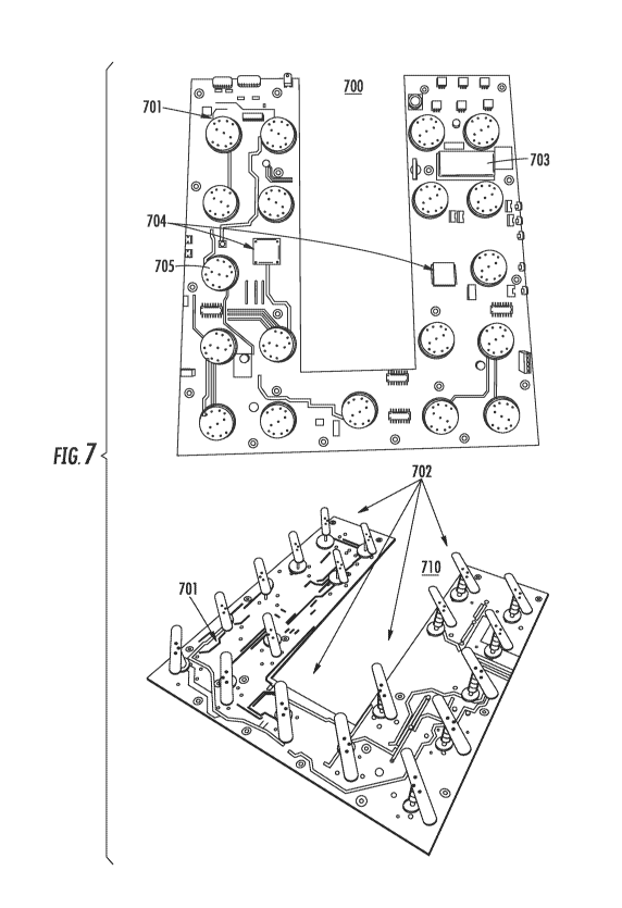
[0069] Fig. 7 provides a plan view 700 of the front side of a printed circuit
board 701
along with an isometric view 710 of the back side of the printed circuit board
701.
Printed circuit board 701 is configured to be mounted to an electronic oven
such that the
array of variable reflectance elements 702 can serve as the set of variable
reflectance
elements 608 in Figs. 6a-6b. The printed circuit board in the illustrated case
is in a u-
shape. However, the printed circuit board can take on any other shape
depending upon
the pattern of variable reflectance elements used. The front side of the
printed circuit
board 701 includes power regulation circuits 703 and control logic circuits
704. The
control logic circuits 704 can be ARM processors or equivalents. The front
side of the
printed circuit board also includes multiple drive motors 705 which can
exhibit the same
features as drive motor 311 from Fig. 3. The drive motors can each
individually rotate a
corresponding variable reflectance element in array 702 based on instructions
provided
from control logic circuits 704 and stored on those logic circuits.
27
CA 03007485 2018-06-04
WO 2017/218387 PCT/US2017/036970
[0070] Fig. 8 provides two detailed views of an individual variable
reflectance element
801 in array 702. In view 800, the reflective element is shown on PCB 701 with
motor
drive shaft 802 mated to drive shaft connection cylinder 303 of dielectric
spindle 201.
Drive shaft 802 can be part of a drive motor and may be made of metal. The PCB
is
then mounted in such a way that the drive shaft 802 does not extend into the
chamber
of the electronic oven, and only the thicker portion 803 of the dielectric
spindle extends
into the chamber.
[0071]View 810 provides an example of how the dielectric spindle could be
positioned
with respect to the chamber of the electronic oven. The spindle could extend
through a
perforation 811 in a surface of the chamber 812. The perforation could be
punched in
the surface of the chamber or formed by laser cutting. The perforation could
be made
small enough that a tight seal was formed with dielectric spindle 803 to avoid
any
energy leaking out of the chamber. The fact that the dielectric spindle is
thicker above
the point at which it extends into the chamber further assists in assuring
that energy
does not leak from the chamber. The length of the thick portion of the
dielectric spindle
would then set the distance at which the reflective element of the variable
reflectance
element was held off from the surface of the chamber.
[0072] Fig. 9 provides a view of the set of reflective elements 702 once PCB
701 is
mounted to the electronic oven. The view is from the bottom of the chamber of
the
electronic oven looking up at the ceiling of the chamber. The thick portion of
each
dielectric spindle and the reflective elements are seen extending through
perforations in
surface 900. PCB 701 is set off from the chamber such that the thick portion
of each
dielectric spindle nearly rests on surface 900. Antenna 901 is a dual patch
antenna and
28
CA 03007485 2018-06-04
WO 2017/218387 PCT/US2017/036970
is coupled to an injection port in the chamber. Fig. 10 is the same view of
the chamber
with a false ceiling 1000. The false ceiling could be made of plastic such as
polypropylene or some other material that is transparent to microwave energy.
The
antenna and set of reflective elements are not visible because they are
positioned
behind false ceiling 1000 such that they are shielded from splatter or other
interference.
[0073] The reflective elements can be held above a surface of the chamber at a
specific
distance that depends on the wavelength of the electromagnetic energy and is
selected
to maximize the interference introduced by the reflective elements. As shown,
the
surface of the reflective elements defines a plane that is offset from the
surface of the
chamber. The vertical spacing as measured perpendicular to the surface of the
chamber and the false ceiling is less than 0.6 of the wavelength of the
shortest
electromagnetic wave introduced to the chamber. In the approach illustrated by
Fig. 9
the plane defined by the surface of the reflective elements is approximately
25 mm from
the surface of the chamber which equates to a distance of roughly a quarter
wavelength
for the electromagnetic energy for which the electronic oven of Fig. 9 is
designed to
receive. The spacing is selected to maximize the interference caused by the
variable
reflectance elements with the electromagnetic energy introduced to the chamber
and
therefore the variability of the patterns of electromagnetic distribution in
the chamber
available to a control system for the electronic oven. The specific distance
at which the
reflective elements are held off from the wall of the chamber can be variable
if the
electronic oven is designed to introduce electromagnetic waves of different
frequencies
into the chamber. The drive shafts can be mechanically extendible to allow for
this
effect.
29
CA 03007485 2018-06-04
WO 2017/218387 PCT/US2017/036970
[0074]As illustrated, the antenna is likewise spaced off from the surface of
the chamber.
In the approach illustrated by Fig. 9, the antenna is approximately 13 mm from
the
surface of the chamber. However, this spacing is set by the geometry of the
antenna
and is generally independent of the optimal spacing for the reflective
elements. As such,
the fact that the spacing of the array can be irregular provides significant
benefits from a
design perspective as the array can be interrupted to provide room for the
antenna if it
happens that the antenna and reflective element perform best in two regions of
vertical
spacing that would otherwise conflict.
[0075]As mentioned previously, the set of reflective elements can be placed on
any
surface or surfaces of the electronic oven. However certain benefits accrue to
approaches in which the reflective elements are located on the same side of
the
chamber as the injection port and opposite the item to be heated as in
electronic oven
430. The benefit relates to the fact that most items placed in an electronic
oven for
heating only absorb a relatively small amount of energy on a first pass of the
electromagnetic wave. For example, a cup of tea placed in an electronic oven
in which
energy is delivered from a ceiling injection port only absorbs 10-15% of the
electromagnetic energy on a first pass, and roughly 80% of the energy is
reflected back
up to the ceiling. Therefore, placing the set of reflective elements on the
ceiling is
beneficial in that it interferes with the outgoing wave as soon as it is
delivered to the
chamber, and it is directly in line with a large amount of the energy as it
reflects off the
item. The effect continues for each subsequent reflection and is compounded by
the
fact that the bulk of the energy is delivered perpendicular to the plane set
by the
reflective elements.
CA 03007485 2018-06-04
WO 2017/218387 PCT/US2017/036970
[0076] In the above approaches, a single injection port was utilized to
introduce energy
into the chamber. However, multiple injection ports and energy sources could
be
utilized to introduce energy into the chamber. These alternative approaches
would still
be in keeping with the approaches of Figs. 6a and 6b so long as the elements
in the set
were non-radiative and did not introduce additional energy to the chamber. In
particular, the chamber could include two injection ports above item 606, or
injection
ports both above and below item 606 such that heat could be directed to the
item from
multiple directions. Each injection port could be connected to the same
microwave
energy source, such as a single magnetron, or could have its own associated
microwave power supply. As before, the chamber would still not receive any
microwave
energy besides the microwave energy from the injection port and the second
injection
port.
[0077] The illustrated spacing of elements in set 608 is not exhaustive. As
mentioned,
the elements can be spaced in numerous ways. In particular, the set can be
spaced to
create a diffraction grating with a variable angle of reflection by
deactivating certain
elements of the array. Further, the set can be spaced so that different sub-
sets or
patterns can be deactivated for purposes of steering electromagnetic energy
with
different wavelengths. With reference to the spacing discussion above, the
elements
can also be spaced so that they are spaced apart by at least one half of the
wavelength
of the shortest wavelength of energy supplied to the chamber from the energy
source.
Again, the set can be configured in an array, but the array can have
interrupts for
features of the electronic oven such as a waveguide impression in the chamber
surface,
a camera, or a mode stirrer. For example, in situations in which the
electronic oven
31
CA 03007485 2018-06-04
WO 2017/218387 PCT/US2017/036970
included two injection ports, the array could be adjusted to provide space for
two offset
antennas on a ceiling of the microwave oven.
[0078]The set of variable reflectance elements can continue to provide a
significant
number of useful distributions of energy in the chamber despite being
irregularly
spaced. Fig. 9 is an example of this flexibility in that the illustrated set
of reflective
elements includes 19 elements in a 5x5 array with elements removed to make
space for
an antenna 901 and a camera 902. Increasing the density does tend to increase
the
flexibility of the control system, but the returns diminish and eventually
drop to near zero
when the spacing becomes less than one half the wavelength of the smallest
electromagnetic wave introduced to the chamber. In the illustrated case of
Fig. 9, the
array pitch is 63 mm which was selected in light of a microwave energy source
introducing an electromagnetic wave at a frequency of 2.45 GHz to the chamber,
which
corresponds with a half wavelength of 59 mm.
[0079]ARRAY FUNCTIONALITY
[0080]A set of methods for heating an item in a chamber can be described with
reference to flow chart 1100, diagram 1110, and diagram 1120 in Fig. 11. Flow
chart
1100 includes a step 1101 of applying a first electromagnetic wave to the
chamber from
an energy source to a set of variable reflectance elements. The methods of
flow chart
1100 can be applied to the configurations described above. The set of variable
reflectance elements can include a set of variable impedance devices or a set
of
movable reflective elements. The variable impedance devices could be solid
state
32
CA 03007485 2018-06-04
WO 2017/218387 PCT/US2017/036970
devices. Step 1102 involves reflecting the first electromagnetic wave from the
set of
variable reflectance elements to the item. Steps 1101 and 1102 are illustrated
as
sequential steps but they could both be occurring in a looping and/or
simultaneous
manner. In this sense, the electromagnetic wave could be an amount of energy
produced by the energy source in an arbitrary period of time.
[0081] Diagram 1110 illustrates the first electromagnetic wave 1103 being
delivered to a
first variable reflectance element 1104 and a second variable reflectance
element 1105.
The first electromagnetic wave could be incident on the elements directly from
the
injection port in the chamber or could be a reflection from elsewhere in the
chamber.
The concentric circles radiating out from elements 1104 and 1105 represent the
reflected electromagnetic energy that is produced in step 1102. Specifically,
each circle
represents a local maximum magnitude of reflected energy. In diagram 1110, the
two
elements produce patterns with identical phases such that the inner most
circle of the
set has the same radius. As a result, the two reflected signals combine to
produce an
energy distribution pattern with an antinode at location 1107. The energy
distribution
will include many such local maximums. In particular, the energy distribution
pattern
may place a local maximum of energy at a first location on the item being
heated in the
chamber.
[0082] In step 1115, a reflectance of one of the variable reflectance elements
is altered.
As used herein, the term "reflectance" is used with reference to the
reflection coefficient
as it is defined in the field of telecommunications. The coefficient is
calculated using the
impedance of the load and source at the point of reflection. It is a complex
number with
both a magnitude and phase. The reflectance of the variable reflectance
element can
33
CA 03007485 2018-06-04
WO 2017/218387 PCT/US2017/036970
be modified in numerous ways as will be described below. In particular, one
way is to
alter the impedance of an optional solid-state device associated with the
variable
reflectance element. In other words, step 1102 may be conducted when a first
solid
state device in the array of solid state devices has a first impedance value,
and step
1115 can include altering the impedance of the first solid state device to a
second
impedance value. In another example, the orientation of the variable
reflectance
element can be altered by physically repositioning the variable reflectance
element. In
certain approaches, a 900 rotation of the variable reflectance element will
change the
phase of the wave reflected from the variable reflectance element. In other
words, step
1102 may be conducted when an electrically reflective element is oriented in a
first
position and step 1115 can include rotating the reflective element from the
first position
to a second position.
[0083] Flow chart 1100 then continues to step 1121 in which a second
electromagnetic
wave is applied to the chamber from the energy source. The second and first
electromagnetic waves can be two different portions of the same continuous
supply of
energy at two different times. In other words, the energy source does not need
to vary
in terms of the power and direction of application. Therefore, with reference
to diagram
1120, the second electromagnetic wave 1113 can have the same general
characteristic
as the first electromagnetic wave 1103 from diagram 1110.
[0084] Step 1122 involves reflecting the second electromagnetic wave from the
set of
variable reflectance elements to the item. To illustrate this step, diagram
1120 again
includes variable reflectance elements 1104 and 1105. As mentioned previously,
second electromagnetic wave 1113 can have the same general characteristic as
first
34
CA 03007485 2018-06-04
WO 2017/218387 PCT/US2017/036970
electromagnetic wave 1103. However, since the reflectance of one of elements
1104
and 1105 has changed, the location of the local maximum has moved from
location
1107 to location 1114. As illustrated, the change in the reflectance of
variable
reflectance element 1105 resulted in a phase shift in the reflectance. This is
illustrated
by the fact that the first local maximum of the energy reflected by element
1105 is
physically closer to the center of the element. Using this approach, step 1122
can
cause the location of the local maxima of the distributed energy pattern in
the chamber
to alter their locations. In particular, the location of a local maximum on
the item being
heated can be altered from a first location to a second location where the
first and
second locations are different.
[0085] In diagram 1120, where the reflectors are ideal point reflectors and do
not involve
moving parts, the location of local maxima could at most be modified by up to
one
wavelength. However, if the reflectance of multiple variable reflectance
elements in the
array can be modified, then the local maxima can be moved with a much greater
degree
of flexibility. In a basic example, flow chart 1100 could include step 1130 in
which the
reflectance of a second variable reflectance element is modified. The step is
shown in
phantom because it could be conducted before, after, or simultaneously with
step 1115.
Depending upon the control system that is configured to interface with the
variable
reflectance elements, the variable reflectance elements in the array could
each be
modified independently, they could be modified in groups, or they could be
modified in
an interrelated manner. For example, element 1104 could have its reflectance
altered
at the same time as element 1105 but with a phase change in the opposite
direction to
double the effect of the modification.
CA 03007485 2018-06-04
WO 2017/218387 PCT/US2017/036970
[0086] The reflectance of each variable reflectance element can be changed in
different
ways depending upon the application. For example, the reflectance could be
adjusted
such that the phase of the reflectance was tuned continuously between 0 and
180 by
steps, such as steps of one degree, or could be hard switched to specific
values such
as 0 , 900, and 180 . In addition, both the phase and magnitude of the
reflectance could
be altered. Each variable reflectance element could be associated with a
variable
impedance device to provide the associated variation in reflectance. In
particular, each
variable reflectance element could be associated with a solid-state device
such as a
PIN diode or FET to provide the associated variation in reflectance. Using the
example
of a FET, the voltage on the control gate could be swept continuously between
two
voltages to alter the impedance of the load that sets the reflectance
coefficient. Again
with reference to the FET example, the voltage could be switched between a
lower and
upper reference voltage to turn the FET all the way on or off to alternatively
connect the
main body of the variable reflectance element to another circuit node or keep
it floating.
Using the example of an electrically reflective element that can be moved to
various
positions, the phase and magnitude of the reflectance can be altered by
altering the
orientation of the element with respect to the polarization of the incident
wave. The
element could be configured to switch between physical positions separated by
variable
step sizes that correspond to desired changes in the phase of the reflectance.
Alternatively, the electrically reflective element could be moved to various
fixed
positions according to a regular pattern such as by rotating in a circle by 10
, 45 , or 90
intervals. The controller could be configured to rotate the element and keep
track of its
current position value by summing the number of fixed rotation steps taken.
36
CA 03007485 2018-06-04
WO 2017/218387 PCT/US2017/036970
Alternatively, the controller could be configured to rotate the element to
certain fixed
locations and keep track of its current position directly by storing the fixed
value to
which the element was moved.
[0087] Fig. 12 illustrates a flow chart 1200 for a set of methods that can be
utilized to
execute method steps 1101 and 1121 in flow chart 1100. Flow chart 1200 begins
with
step 1201 in which AC power is received from an AC mains voltage source. This
step
can be conducted by energy source 1101 operating in combination with optional
power
conditioning and conversion circuitry. The term AC mains voltage source is
meant to
include all worldwide standard AC voltages and frequencies including the
standard 120
V at 60 Hz AC mains voltage source utilized in the United States.
[0088] Flow chart 1200 continues with step 1202 in which the AC power is
converted to
microwave energy. This step can be conducted using a magnetron in energy
source
601. The step can be conducted by numerous other power conversion options such
as
through the use of inverter technology and the use of solid state devices. As
such, the
frequency, amplitude, and polarization of the microwave power can be varied
through a
single heating session. Step 1202 can also include the use of multiple
microwave
energy converters in a single electronic oven.
[0089] Flow chart 1200 continues with step 1203 in which microwave energy is
delivered to the chamber via an injection port in the chamber. The microwave
energy
generated in step 1202 can be delivered to the injection port using a
waveguide from
the microwave converter to the injection port. The injection port and
waveguide could
be elements 603 and 604. The energy could also be channeled to multiple
injection
37
CA 03007485 2018-06-04
WO 2017/218387 PCT/US2017/036970
ports in the chamber using multiple waveguides. These approaches could be
combined
with those in which multiple microwave converters were utilized in step 1202.
[0090] Flow chart 1200 then returns to step 1102 or 1122 in flow chart 1100
where the
applied energy is reflected from the set of variable reflectance elements. The
set of
variable reflectance elements only receives microwave energy via the chamber
from
energy generated by the energy source. For example, in situations where the
energy
source is a magnetron, the magnetron generates all of the microwave energy
that will
be delivered to the chamber, and delivers all of it via the injection port, or
ports, in the
chamber. In other words, additional waveguides do not provide power to the
elements
of the array of variable reflectance elements. In these approaches, the
chamber does
not receive any microwave energy besides the microwave energy from the
injection
port. Therefore, the elements of the array of variable reflectance elements
are non-
radiative elements. There is no way for the elements to radiate energy into
the
chamber, they only reflect energy provided to the chamber.
[0091] SET COMPOSITON
[0092] The set of variable reflectance elements in the chamber can be arranged
as an
array, or arrays, with various characteristics in order to serve their purpose
in varying
the phase of the energy they reflect and thereby virtual resize the chamber.
Each
variable reflectance element in a set of variable reflectance elements could
correspond
with a variable impedance device. Each variable reflectance element in a set
of
variable reflectance elements could correspond with an electrically reflective
element.
38
CA 03007485 2018-06-04
WO 2017/218387 PCT/US2017/036970
In certain approaches, each variable reflectance element in an array of
variable
reflectance elements could uniquely correspond with a variable impedance
device. The
variable impedance devices could be solid state devices. The variable
reflectance
elements may include a reflective element that is attached to a wall of the
chamber
using a conductive or insulating support. The reflective element can be formed
of sheet
metal. The reflective element could be connected to either a ground plane or
another
variable reflectance element via a variable impedance device. The variable
impedance
devices could be located on a wall of the chamber. For example, the variable
impedance devices could be located on a PCB on a wall of the chamber, or could
be
housed in a structure connecting the body of the variable reflectance element
to the
wall. The ground plane could be a wall of the chamber or a metal layer on a
printed
circuit board. The metal layer could be copper.
[0093]As mentioned previously, the reflectance of the variable reflectance
elements can
be altered to adjust the phase of the reflected energy. The reflectance could
be
adjusted in response to a control system located in or on the electronic oven.
To this
end, the variable reflectance elements can be altered from a first state to a
second
state. The variable reflectance elements can be defined by binary states and
serve as
digital tuners for the reflected energy or may be able to transition
continuously between
a large number of states and serve as analog tuners for the reflected energy.
For
example, the phase shift introduced by each variable reflectance element could
be from
0 to 90 and back, or could be anywhere from 0 to 180 with a smooth
transition
between each gradation on the spectrum. As another example, the orientation of
each
variable reflectance element with respect to the dominant polarization of an
incident
39
CA 03007485 2018-06-04
WO 2017/218387 PCT/US2017/036970
electromagnetic wave could be changed from 00 to 900 and back, or could be
anywhere
from 00 to 1800 with a smooth transition between each gradation on the
spectrum.
Notably, even in the binary case, the variable reflectance element is only one
element in
a set, so the number of elements can be increased to provide flexibility to
the control of
the reflected energy despite the fact that each individual element only has
two states.
[0094] The controller could be designed to store the state of each variable
reflectance
element in order to make that data available to a higher-level control system
tasked with
determining the optimal distribution of energy in the electronic oven at any
given time.
The value could be stored after each adjustment so that a current state value
was
updated after each action that changed the state of the element. In the
particular
example of a variable reflectance element with an electrically reflective
element that
changed its physical position, the controller could store a corresponding
current position
value independently for each reflective element in the set of reflective
elements used in
the chamber. The controller could then also store instructions that alter the
corresponding current position values in response to a movement, such as a
rotation of,
the set of reflective elements. For example, if the variable reflectance
element was
undergoing a change in position from a first position to a second position,
the current
position value could be changed from a value corresponding to the first
position to a
value corresponding to the second position. In order to accurately track this
information, each action taken by the controller would need to be carefully
undertaken
to assure that the stored value for the state of the variable reflectance
element
accurately reflected the real-world state of that element. Alternatively, the
mechanism
for setting the state of the variable reflectance elements could be designed
to be
CA 03007485 2018-06-04
WO 2017/218387 PCT/US2017/036970
tracked easily such that a single stored variable could reflect its current
state. In the
specific example of an element positioned by an actuator such as drive motor
311, the
position of each actuator could be a variable at a memory location in RAM. The
memory location could be accessible to or readable by the actuator. Adjusting
the
position of the element would then involve writing a new value to that memory
location,
and allowing the actuator to access the memory location and move the element
to the
new location.
[0095]As stated previously, the controller could be control logic such as ARM
processors located on a circuit board in the electronic oven, and the position
of a
reflective element could be set by a gauge motor that receives instructions
from the
control logic via the circuit board. In approaches in which the reflective
elements are
formed by thin sheet metal aluminum, the low torque provided by gauge motors
would
not an issue because of the light weight of the reflective elements.
Furthermore, gauge
motors are designed to receive instructions to reliably rotate to a specific
location such
that the controllers can easily keep track of what position each reflective
element has
been rotated to. This feature would facilitate the operation of the overall
control loop for
the electronic oven.
[0096]The potential states for the electrically reflective elements could be
stored ex
ante by the controller and recalled when the controller was operational. For
example, a
set of fixed positions could be stored for an electrically reflective element
that was
configured to alter its position such as at 900" or at baseline." The
controller could
then recall these values and implement them using a motor when it was time to
place
the variable reflectance elements in a given condition.
41
CA 03007485 2018-06-04
WO 2017/218387 PCT/US2017/036970
[0097] In certain approaches, to avoid unwanted absorption or dissipation of
the
microwave energy in the variable reflectance elements, the variable
reflectance
elements are designed to have a substantially reactive impedance at the
frequency, or
frequencies, of energy applied by the energy source. This ensures that the
incident
energy is effectively reflected and used for heating the item, rather than
causing
unwanted loss or heating in the variable reflectance elements themselves. In
certain
approaches, this will involve maintaining the low impedance state of any
variable
impedance devices needed to alter the state of their associated variable
reflectance
elements at an impedance less than 1 Q.
[0098]Additionally, certain steps can be taken to assure that the variable
reflectance
elements do affect the amplitude of the reflected energy. In certain
approaches, it may
be beneficial to allow the variable reflectance elements to absorb energy and
pull it out
of the chamber via one or more of the variable reflectance elements in order
to achieve
balance in the chamber. For example, a subset of variable reflectance elements
may
include a variable impedance device that wires the variable reflectance
element to an
injection port in the chamber wall. The variable impedance device could
exhibit a high
impedance to energy at the frequency of the energy applied to the chamber in a
neutral
state, but exhibit a low impedance at that same frequency when it was time for
the
associated element to remove energy from the chamber.
[0099]The reflectance of the variable reflectance elements can be altered to
modify the
characteristics of the chamber in order to accommodate different frequencies
for the
energy applied to the chamber. In some approaches, the frequency of the energy
applied to the chamber will have an appreciable effect on how that energy
responds to
42
CA 03007485 2018-06-04
WO 2017/218387 PCT/US2017/036970
the variable reflectance elements. For example, an array that is configured to
tune
energy delivered at a first frequency in order to move a local maximum of the
distributed
pattern of energy 10 cm in any direction will be unable to move a local
maximum more
than a single cm at a second frequency. As a result, the array will be unable
to
appreciably alter the position of the local maxima to achieve even heating in
the
electronic oven. To alleviate this problem, different arrays can be formed in
the
chamber to deal with different frequencies of applied energy. The different
arrays can
be subsets of each other where the unused elements of one array are locked at
a
neutral state when the second array is operating. The neutral state could be
set to
mimic the reflectance of the bare wall of the chamber at the current frequency
of applied
energy, or could be set to perfectly reflect all energy with zero change in
the phase or
magnitude.
[0100]In certain approaches, the set of variable reflectance elements can
include a set
of electrically reflective elements that physically alter their position. For
example, the
variable reflectance elements could include a reflective element that is held
above a
surface of the chamber by a dielectric support. The reflective element could
be formed
by sheet metal. The dielectric support could be a dielectric spindle used to
rotate the
reflective element. Rotation could be conducted around a central axis normal
to a wall
of the chamber or parallel to a wall of the chamber. The axis could also be
offset from
the chamber wall at a different angle.
[0101]Fig. 13 illustrates block diagrams that provide an explanation of how
step 1115
can be conducted in accordance with the description provided immediately above
regarding the variable reflectance elements. In step 1300, a variable
reflectance
43
CA 03007485 2018-06-04
WO 2017/218387 PCT/US2017/036970
element is altered from a first state to a second state. These two states
could describe
all of the states that the variable reflectance element could exhibit, or they
could be two
from among multiple states. In step 1301, an impedance of a variable impedance
device is altered. The variable impedance device could correspond with the
variable
reflectance element and could correspond with the variable reflectance element
uniquely. In step 1302, a physical position of a variable reflectance element
is altered
from a first position to a second position.
[0102]Fig. 13 includes block diagrams of specific ways in which step 1301
could be
executed. In diagram 1303, a variable reflectance element body is left
floating in one
state and is connected to ground in a second state. As a result, the time it
takes charge
to flow from one end of the device to the other is altered and the phase of
the
reflectance will change. In another approach, illustrated by reference number
1304, the
variable impedance element is a varactor and the change in capacitance alters
the
phase of the reflected energy. The approach illustrated by reference number
1305
expands this concept to indicate that any complex impedance can be made
variable to
alter the reflectance of the variable reflectance element. More specific
examples are
provided below with respect to Figs. 14-20. In diagram 1306 of Fig. 13, a
variable
reflectance element comprises an electrically reflective element that is
rotated 90 to
change its orientation with respect to the polarization of an incident wave of
electromagnetic energy. The axis of rotation in this case is normal to a wall
of the
chamber such that diagram 1306 is a plan view of that wall. In diagram 1307, a
variable
reflectance element comprises an electrically reflective element that is fixed
on one end
44
CA 03007485 2018-06-04
WO 2017/218387 PCT/US2017/036970
and rotated by extending a support connected to an opposite end. More specific
examples are provided below with respect to Figs. 21-22.
[0103]The body of the variable reflectance elements can be configured in
accordance
with the structure utilized for various types of antennas. For example, patch,
dipole,
monopole, slot, or split ring resonator antenna structures could be employed
to form the
body of the variable reflectance elements. However, the use of additional
physical
structures associated with radiative devices would generally not be needed. In
a
specific example, the variable reflectance element could be a monopole
reflector with
an optional connection to ground via a variable impedance device. In another
example,
the variable reflectance element could be configured as a single portion of
two adjacent
monopoles in a bowtie configuration with a variable impedance connection
between the
two halves. In this approach, a single variable impedance device would adjust
the
reflectance of two variable reflectance elements by isolating them in one
state and
wiring them together in another state. The array may include a mix of
different
structures for its composite elements such as a mix of monopoles and dipoles
in a
repeating pattern.
[0104]The variable reflectance elements could be configured to operate in two
or more
states. One of those states could involve the body of the device floating and
another
state could involve the body being wired to ground. Alternatively, one of
those states
could involve the body of the device floating and another state could involve
the body
being wired to another variable reflectance element. In a still further
approach, the
device could exhibit more than two states and those states could include being
left
floating, being wired to a ground plane, and being wired to one or more other
variable
CA 03007485 2018-06-04
WO 2017/218387 PCT/US2017/036970
reflectance elements. To compound the number of states each element can
exhibit, an
associated variable impedance device used to transition the device between
these
various states could itself exhibit more than two states. In other words, the
variable
impedance device could isolate the body of the variable reflectance element,
wire it to
another node, or connect it to a node via an intermediate impedance.
[0105]Fig. 14 illustrates an example variable reflectance element 1400 both
from a side
view (top image of Fig. 14) and plan view (bottom image of Fig. 14). Element
1400
alters a phase shift provided by the device by alternatively floating or being
wired to a
ground plane. Element 1400 includes a body 1401 in the shape of a monopole
antenna
and a variable impedance device 1402 embedded in a support structure 1403. The
support structure is connected to ground plane 1404. The ground plane could be
a wall
of the chamber or a conductive layer on a printed circuit board that is placed
on the wall.
Variable impedance device 1402 could be a switch such as a PIN diode or FET.
The
switch could alter between two states which would likewise cause the variable
reflectance element 1400 to alter between two states with different
reflectance. In a first
state, the switch would be open and have a high impedance, and the body 1401
would
be floating. In a second state, the switch would be closed and have a low
impedance,
and the body 1401 would be wired to ground plane 1404. Ground plane 1404 could
be
specific to device 1400 or it could be shared by multiple variable reflectance
elements.
An element with the same configuration could also exhibit multiple phase
shifts if an
impedance of variable impedance device 1402 could be gradually modified. The
device
could also be modified to have multiple associated variable impedance devices
that
could connect the body of the device to the ground plane at different
locations.
46
CA 03007485 2018-06-04
WO 2017/218387 PCT/US2017/036970
[0106] Fig. 15 illustrates another example variable reflectance element 1500
both from a
side and plan view. Element 1500 alters a phase shift provided by the element
by
alternating at what point along the length of body 1501 the body 1501 is wired
to a
ground plane 1502. Element 1500 again includes a variable impedance device
1503
embedded in a structure 1504. However, element 1500 includes an additional
conductive structure 1505 that constantly wires body 1501 to ground. Variable
impedance device 1503 can exhibit the same characteristics as element 1502
above
and can respond to a similar control signal. However, the effect on the
reflectance of
variable reflectance element 1500 will be different because of the fact that
body 1501 is
continuously wired to ground.
[0107] In one approach, element 1500 is approximately X/4 long from the point
at which
it is permanently terminated to ground at 1505 to the alternative end at point
1506. In
this case (grounded at only one end), element 1500 acts as a resonant element,
and
the reflected wave is in-phase with the incident wave. When variable impedance
device
1503 is switched it creates an additional termination to the ground plane
further along
the electrical length of body 1501. Element 1500 is thereby switched from one
state to
another. In this situation, element 1500 becomes non-resonant, and the
dominant
reflection is from the conductive ground plane. The reflected wave is now out
of phase
with the incident wave, resulting in a substantial phase shift in the
reflected energy. In
one approach, the phase shift is nearly 180 degrees (n radians).
[0108] Structures 1504 and 1505 can both be support structures or only one can
be a
support structure while the other merely provides a conductive electrical
connection. In
47
CA 03007485 2018-06-04
WO 2017/218387 PCT/US2017/036970
particular, structure 1505 could be a weld point that welds body 1501 to
ground plane
1502.
[0109]Fig. 16 illustrates a pair 1600 of example variable reflectance elements
from a
side and plan view. Element 1600 alters a phase shift provided by the pair of
variable
reflectance elements by alternating between a connected and unconnected state.
As
illustrated the pair 1600 of variable reflectance elements include body 1601
and body
1602. The two bodies rest on support 1603. Support 1603 is insulating and does
not
conduct RF energy. As such, structure 1604 does not need to be a ground plane.
However structure 1604 could still be the wall of the chamber or a specialized
surface
formed thereon. The pair of devices 1601 and 1602 share another structure 1605
with
an embedded variable impedance device. As the variable impedance device alters
between an open and a closed state, the pair of variable reflectance elements
of
element 1600 will each change their reflectance in that they are transitioning
from a
state in which they are floating to a state in which they are wired to an
adjacent variable
reflectance element. In the illustrated embodiment, the overall structure will
remain
floating, but each individual element can be conceptualized as no longer
floating
because it is connected to an external structure that will affect its bias
point. The
devices could also each be modified to have multiple associated variable
impedance
devices that would connect the body of the device to the other device at
different
locations.
[0110]Fig. 17 illustrates a set of example variable reflectance elements 1700
from a
plan view. The set of devices includes four monopole antenna elements 1701,
1702,
1703, and 1704 that are all resting on a single insulating support structure
1705. As
48
CA 03007485 2018-06-04
WO 2017/218387 PCT/US2017/036970
with Fig. 16, the underlying structure 1706 does not need to be a ground
plane, but it
can still be the wall of the chamber or a specialized surface formed thereon.
The
devices are connected together via a network of variable impedance devices
1707. The
controls system that alters the state of the switches in network 1707 could be
able to
adjust the switches independently. As the reflectance of each element will be
affected
not only by which elements it is connected to, but by which elements those
elements
are in turn connected to, the number of potential reflectance values that the
set of
devices can exhibit can be described by 64 different states.
[0111]Fig. 18 illustrates an example variable reflectance element 1800 from a
side and
plan view. As illustrated, the device includes a body 1801 in the shape of a
slot antenna
with a slot 1802. The width of slot 1802 (vertical dimension of slot 1802 in
Fig. 18) can
be much less than the wavelength of the energy applied to the chamber by the
electronic oven. The length of the slot 1802 (horizontal dimension) can be
appreciable
compared to that wavelength. In particular, the length of slot 1802 could be
half that
wavelength. Body 1801 could be sheet metal or some other conductive material
that
can serve as a ground plane. Device 1800 also includes support structures 1803
that
separate body 1801 from layer 1804. The support structures 1803 could be
separate
structures or they could be two portions of one contiguous piece of material.
The
support structure could be insulating material. The layer 1804 can be a wall
of the
chamber or a layer placed on the wall. In an alternative approach, body 1801
itself
could be the wall of the chamber itself or a layer placed directly on the
wall. In the latter
case, slot 1802 could be a portion of the wall exposed by the removal of that
layer. In
the former case, slot 1802 could be an excavated portion of the wall such as a
divot in
49
CA 03007485 2018-06-04
WO 2017/218387 PCT/US2017/036970
the wall structure or a valley-shaped bend in the exterior of the wall.
Element 1800 also
includes a variable impedance device 1805 that can serve to alter the phase
shift
imparted to impending energy.
[0112]Variable impedance device 1805 could be a switch such as a PIN diode or
FET.
The switch could alter between two states which would likewise cause the
variable
reflectance element 1800 to alter between two states with different
reflectance. As the
variable impedance device alters between an open and a closed state, the
variable
reflectance element 1800 will alter the phase shift applied to impending
energy because
the effective length of slot 1802 as compared to the wavelength has been
altered. The
fact that the currents around the slot through body 1801 now have two looping
paths
they may take around the slot will also alter the reflectance of device 1800.
[0113]Fig. 19 illustrates an example variable reflectance element 1900 from a
side and
plan view. The side view is cross sectional and is taken from reference line A
on the
plan view. The illustrated variable reflectance element 1900 is an example of
one of the
embodiments described above, where slot 1901 is formed by an excavated portion
of
the wall 1902 in the form of a perforation. Wall 1902 could be a continuous
layer of
sheet metal perforated with slots like slot 1901. Layer 1904 can be a solid
wall of
material such as sheet metal. Alternatively, layer 1904 can comprise one of
numerous
pockets placed on the back of wall 1902 in the vicinity of the perforations to
prevent the
leak of microwave energy from the chamber. The dimensions of slot 1901 can be
similar to those of slot 1802. The depth of slot 1901 could be A/4 where X is
a
wavelength of energy applied to the chamber. For example, the wavelength of
the
wave of energy applied to the chamber with the shortest wavelength. Variable
CA 03007485 2018-06-04
WO 2017/218387 PCT/US2017/036970
impedance device 1905 could exhibit the same physical and operational
characteristics
as variable impedance device 1805.
[0114]The individual elements of the array could be spaced, distributed, and
oriented
across the wall of the chamber in various ways. As mentioned previously, the
array
might cover every wall of the chamber, be limited to a single wall, or span
multiple walls.
There may also be multiple arrays in the chamber with their own varying
spacing,
distribution, and orientation. Also as mentioned previously, elements in the
array could
be placed at the center of every square inch on a wall of the electronic oven.
However,
the density could also be less than one element per square inch such as less
than one
element per every 6 square inches. To the extent the individual elements are
not
symmetrical around a center point, the orientation of the individual elements
relative to
each other could be constant or could be varied from element to element within
the
chamber. In implementations in which the orientation of the individual
elements was
constant, the orientation could vary in different implementations relative to
the chamber
itself. For example, all of the elements could be oriented along the x, y, or
z-axis of the
chamber.
[0115]The orientation of the individual elements can be altered throughout the
array so
that a particular polarization is not favored. For example, Fig. 20 provides
an illustration
of an array 2000 of variable reflectance elements in the style of Fig. 18 that
are
distributed with two different orientations in a repeating pattern across the
array. As
illustrated, one set of elements in the array have a first orientation 2001,
and a second
set of elements in the array have a second orientation 2002. Each element also
includes a variable impedance element 2003 that spans the slot of the element.
Each
51
CA 03007485 2018-06-04
WO 2017/218387 PCT/US2017/036970
element in the array has the same orientation as half of its neighbors and a
different
orientation from the other half of its neighbors. The first orientation and
second
orientation differ by 900. In other approaches, the elements in the array
could have
more than two orientations. The variance in orientation could also be randomly
distributed across the array, or follow a more complex pattern than that
illustrated by
Fig. 20. For example, the orientation could change by a set number of degrees
less
than 90 in a continuous stepwise manner across the array from one neighbor to
the
next.
[0116]The variable impedance elements could be any element that is capable of
exhibiting different impedance values at a given frequency. The variable
impedance
elements could be mechanical or electromechanical devices. The variable
impedance
elements could also comprise passive or active electronic circuitry. The
variable
impedance elements could be a solenoid or relay making a variable physical
connection
to the body of an associated variable reflectance elements. The variable
impedance
elements could be an electromechanical switch with a variable low impedance
capacitive connection.
[0117]Certain benefits accrue to approaches in which the variable impedance
elements
are solid state devices in that there would be a decrease in moving parts
required to
operate in or on the electronic oven. In one example, the variable impedance
elements
could be varactors or a network of passive device with variable impedance such
as
potentiometers or variable inductors. The varactors could be capacitors
designed with a
variable distance between capacitor plates to adjust that capacitance of the
capacitor.
In another example, the variable impedance elements could alternatively
include
52
CA 03007485 2018-06-04
WO 2017/218387 PCT/US2017/036970
switches such as field effect transistors. The switching devices could be any
power
switching device such as a FET, BJT, or PIN diode. In particular, the switches
could be
lateral diffusion metal oxide semiconductor (LDMOS) FETs that were
specifically
applicable for high power applications. In another example, the variable
impedance
devices could be PIN diodes or other devices used for radio frequency or high
power
applications. The power devices could be designed to hold off voltages in the
off state of
greater than 500 V and present an on state resistance of less than 250 mQ.
[0118] In some of the approaches disclosed herein, there is a paucity of
moving parts
required for the electronic oven to deliver energy in a variable manner to the
item being
heated. In certain approaches, the electronic oven does not include any
components
that are in mechanical motion between when the first electromagnetic wave is
applied in
step 1101 and when the second electromagnetic wave is applied in step 1120. In
particular, if the variable impedance devices are solid state devices, they
can alter the
phase of the variable reflectance elements in response to a purely electrical
command
received from the control system and do not need to make any mechanical
movements
in response while still being able to modify the reflectance of the variable
reflectance
elements. Also, since the distribution of energy can be steered using the
array of
variable reflectance elements, more even heating can be achieved without the
use of a
mode stirrer or movable tray for the item to rest on. Furthermore, if a
standard
magnetron is replaced with a microwave energy converter that utilizes solid
state
devices alone, there is the potential for no moving parts to lie on the entire
energy path
from the AC mains voltage to the item being heated.
53
CA 03007485 2018-06-04
WO 2017/218387 PCT/US2017/036970
[0119]Fig. 21 illustrates an example variable reflectance element 2100 both
from a side
view (top image of Fig. 21) and plan view (bottom image of Fig. 21). Element
2100
alters a distribution of energy by altering its physical position from a first
position to a
second position. Element 2100 includes a reflective element 2101 which in this
case is
a relatively flat piece of conductive material that could be formed of sheet
metal such as
aluminum, steel, or copper. The reflective element 2101 is held above a
surface of the
chamber, defined by chamber wall 2102, by a dielectric spindle 2103 that
extends
through a discontinuity 2104 in the chamber wall. The spindle is dielectric,
passes
through a small perforation, and is generally configured to avoid creating an
antenna for
microwave energy to leak out of the chamber. A motor on the exterior of the
chamber is
able to rotate reflective element 2101 via dielectric spindle 2103 by
imparting a force to
the spindle as illustrated by arrow 2105. The force could be applied by a
rotor attached
to spindle 2103. The motor is able to rotate the spindle between a set of
positions
selected from a fixed set of positions. For example, the motor could adjust
the spindle
so that the reflective element 2101 was rotated back and forth through a 90
arc.
[0120]Fig. 22 illustrates a set of variable reflectance elements including
variable
reflectance element 2100 from Fig. 21, and an additional variable reflectance
element
2200. The two elements are shown to illustrate the fact that a set of variable
reflectance
elements in a particular implementation can be treated independently by a
controller,
and further do not need to be uniform elements. In the particular example of
reflective
elements held above a surface of the chamber, the dielectric spindles can hold
the
devices at different heights. Each element in a set of elements could have its
own
unique height. In the illustrated case, the set includes two elements for
purposes of
54
CA 03007485 2018-06-04
WO 2017/218387 PCT/US2017/036970
illustration. However, the set of elements in the chamber can be a set of at
least three
units, and in certain implementations will include many more than three units.
Element
2100 and element 2200 are provided to show that each reflective element can by
associated with a discontinuity, a dielectric spindle, and a motor that are
all unique to
that element. As illustrated, element 2200 could rotate in the opposite
direction 2202 as
the direction of element 2100 which is rotated at the same time.
[0121] Fig. 23 provides an example of the performance of an electronic oven
operating
in accordance with specific approaches described above. Fig. 23 includes two
images
2300 and 2310. Image 2300 shows two eggs that have been evenly cooked in
accordance with an electronic oven generally in accordance with the disclosure
above.
The oven included a set of 19 reflective elements similar to the configuration
shown in
Fig. 9, and was programmed to evaluate the item being heated using an infrared
camera and adjust the reflective elements to evenly apply heat to the eggs.
Image
2310 shows two eggs in the same tray that were placed in a chamber and exposed
to
the same overall level of energy for the same amount of time as the eggs in
image
2300. However, the electronic oven used to cook the eggs in image 2310
attempted to
evenly distribute heat by moving the eggs throughout the heating process on a
traditional rotating tray. The images are fairly self-explanatory. They show
that the two
eggs placed on the traditional rotating tray were not evenly cooked. The yolks
of one of
the eggs ruptured. The consistency of both yolks was not even and the whites
were
burned in several locations. In contrast, the eggs in image 2310 were evenly
cooked
with the yolks exhibiting the same consistency throughout.
CA 03007485 2018-06-04
WO 2017/218387 PCT/US2017/036970
[0122]While the specification has been described in detail with respect to
specific
embodiments of the invention, it will be appreciated that those skilled in the
art, upon
attaining an understanding of the foregoing, may readily conceive of
alterations to,
variations of, and equivalents to these embodiments. Although the specific
cross
sections of the variable reflectance elements showed an associated variable
impedance
device within the chamber, the variable impedance devices could be outside the
chamber and electrically connect to the body of the device via a port in the
chamber.
Any of the method steps discussed above can be conducted by a processor
operating
with a computer-readable non-transitory medium storing instructions for those
method
steps. The computer-readable medium may be memory within the electronic oven
or a
network accessible memory. Although examples in the disclosure included
heating
items through the application of electromagnetic energy, any other form of
heating could
be used in combination or in the alternative. The term "item" should not be
limited to a
single homogenous element and should be interpreted to include any collection
of
matter that is to be heated. These and other modifications and variations to
the present
invention may be practiced by those skilled in the art, without departing from
the scope
of the present invention, which is more particularly set forth in the appended
claims.
56