Note: Descriptions are shown in the official language in which they were submitted.
Data carrier
[0001] The invention relates to a data carrier, e.g. a value document such as
a bank
note, or a security element for securing a value document.
[0002] Data carriers, such as value documents or identification documents, or
other
objects of value, such as branded articles, are for securing often provided
with security
elements which permit a verification of the authenticity of the data carriers
and which at
the same time serve as protection from unauthorized reproduction.
[0003] In this connection there are known (transmission-view) security
elements having
multilayer thin-film elements which upon viewing in incident light, i.e. in
reflection,
appear in a first color and upon viewing in transmitted light, i.e. in
transmission, appear
in a second color. WO 2011/082761 Al describes a thin-film element with
multilayer
structure which appears gold-colored upon the viewing in incident light and
blue upon
the viewing in transmitted light. The multilayer structure is based on two
semi-
transparent mirror layers and a dielectric spacer layer arranged between the
two mirror
layers.
[0004] Any discussion of documents, acts, materials, devices, articles or the
like which has
been included in the present specification is not to be taken as an admission
that any or all
of these matters form part of the prior art base or were common general
knowledge in the
field relevant to the present disclosure.
[0005] Throughout this specification the word "comprise", or variations such
as
"comprises" or "comprising", will be understood to imply the inclusion of a
stated
element, integer or step, or group of elements, integers or steps, but not the
exclusion of
any other element, integer or step, or group of elements, integers or steps.
[0006] Some embodiments of the present disclosure aim to provide a data
carrier of
the kind referred to at the outset having high anti-forgery security and
attractive
visual appearance.
1
CA 3008743 2019-07-25
[0007] Summary
[0008] In one aspect, there is provided a data carrier having a data carrier
substrate and
a security element applied to the data carrier substrate, wherein the side of
data carrier
substrate having the security element defines the front side of the data
carrier and
- the data carrier substrate is a polymer substrate having in the region of
the security
element regions with elevated light transmission and regions with reduced
light
transmission which together form the first motif;
- wherein the regions with reduced light transmission are formed by regions
printed
with opaque ink of the data carrier substrate and the regions with elevated
light
transmission are unprinted regions of the data carrier substrate;
- the security element contains a transparent carrier substrate having a
semi-transparent
function layer, wherein the semi-transparent function layer is constituted
such that (i) the
data carrier upon the viewing its front side in incident light has a first
visually
recognizable color and upon the viewing in transmitted light has a second
visually
recognizable color and (ii) the first motif is imperceptible upon the viewing
of the front
side of the data carrier in incident light and is perceptible upon the viewing
of the data
carrier in transmitted light; and
- the semi-transparent function layer of the security element has a
multilayer construction
with two semi-transparent metallic layers and a dielectric layer arranged
between the two
semi-transparent metallic layers or is obtainable by printing technology by
means of an
effect pigment composition.
[0009] In another aspect, there is provided a data carrier having a data
carrier substrate
and a security element applied to the data carrier substrate, wherein the side
of data
carrier substrate having the security element defines the front side of the
data carrier
and
- the data carrier substrate in the region of the security element has regions
with
elevated light transmission and regions with reduced light transmission which
together
form the first motif; and
- the security element contains a transparent carrier substrate having a semi-
transparent
function layer, wherein the semi-transparent function layer is constituted
such that (i) the
data carrier upon the viewing its front side in incident light has a first
visually
recognizable color and upon the viewing in transmitted light has a second
visually
2
CA 3008743 2019-07-25
recognizable color and (ii) the first motif is imperceptible upon the viewing
of the front
side of the data carrier in incident light and is perceptible upon the viewing
of the data
carrier in transmitted light.
[0010] The first motif upon the viewing of the front side of the data carrier
in incident
light may be perceptible on the basis of lightness differences of the second,
visually
recognizable color.
[0011] The data carrier substrate may be a paper substrate and the regions
with elevated
light transmission are formed by means of thinned paper regions and the
regions with
reduced light transmission are formed by means of thickened paper regions. The
thinned paper regions and the thickened paper regions can form in particular a
watermark.
[0012] The regions with reduced light transmission may be formed by regions
printed
with opaque ink of the data carrier substrate and the regions with elevated
light
transmission are unprinted regions of the data carrier substrate. The regions
printed
with opaque ink can form in particular a watermark generated by printing
technology.
[0013] The alternatives described in the above items for the generating of
regions with
elevated or lowered light transmission, namely the thickened and thinned paper
regions,
on the one hand, and the regions printed with opaque ink and the unprinted
regions, on
the other hand, can furthermore be combined arbitrarily with each other.
[0014] The data carrier substrate may have in the region of the applied
security
element an elevated light transmission compared to the region outside the
applied
security element.
[0015] The data carrier substrate may be a paper substrate which is thinned in
the region
of the applied security element.
[0016] Such a thinning of the paper substrate in the region of the applied
security
element has the advantage that a relatively low intensity of the light source
is enough for
3
CA 3008743 2019-07-25
the achieving of the transmitted light effect.
[0017] The semi-transparent function layer of the security element may have a
multilayer construction with two semi-transparent metallic layers and a
dielectric layer
arranged between the two semi-transparent metallic layers.
[0018] The two semi-transparent metallic layers may be formed independently of
each other from a metal and the metal respectively is chosen from the group
consisting of Al, Ag, Ni, Cr, Cu, Au and an alloy of one or several of the
hereinabove
mentioned elements.
[0019] The two semi-transparent metallic layers may be chosen from Al or Ag
and the
dielectric layer is a SiO2 layer.
[0020] The semi-transparent function layer of the security element may be
obtainable by printing technology by means of an effect pigment composition.
[0021] The security element may have additionally an emboss-lacquer layer
having a
relief structure suitable for the forming of a micromirror arrangement.
[0022] The relief structure of the semi-transparent function layer may form a
second
motif which is perceptible to the viewer at least upon the viewing of the data
carrier in
incident light and preferably is perceptible upon the viewing of the data
carrier in
incident light as well as upon the viewing of the data carrier in transmitted
light. The
second motif may be generated in particular by the semi-transparent function
layer
which is adapted to the emboss-lacquer layer having a relief structure, so
that the relief
structure of the emboss-lacquer layer continues in the semi-transparent
function layer.
[0023] The first motif and the second motif may supplement each other or be in
a
meaningful relation relative to each other.
[0024] The data carrier substrate in the region of the security element may
have, in
addition to the regions with elevated light transmission and regions with
reduced light
4
CA 3008743 2019-07-25
transmission which together form the first motif, a separate window region, in
particular
a recess or a through hole.
[0025] The recess or the through hole can in particular be present in the form
of one or
several microperforations, in particular obliquely extending
microperforations.
[0026] The security element in the window region of the data carrier substrate
may have
an emboss-lacquer layer having a relief structure suitable for forming a
micromirror
arrangement and the relief structure of the semi-transparent function layer in
the window
region forms a (so-called third) motif which is perceptible to the viewer at
least upon the
viewing of the data carrier in incident light and preferably is perceptible
upon the
viewing of the data carrier in incident light as well as upon the viewing of
the data carrier
in transmitted light. The (so-called third) motif may be generated in
particular by the
semi-transparent function layer which is adapted to the emboss-lacquer layer
having a
relief structure, so that the relief structure of the emboss-lacquer layer
continues in the
semi-transparent function layer.
[0027] The security element may be a strip, thread or a patch or label.
[0028] The data carrier may be a value document, such as a bank note, in
particular a
paper bank note, polymer bank note or foil composite bank note, or an identity
document such as an identification card.
[0029] The data carrier itself may be a security element for securing value
documents.
[0030] The security element may be a strip, thread or a patch or label.
[0031] Detailed description
[0032] The data carrier stated in the present description can be a value
document, in
particular a bank note, such as a paper bank note, a polymer bank note or a
foil composite
bank note, or a share, a bond, a deed, a voucher, a check, a high-value
admission ticket,
or an identity document or an identification card, such as a credit card, a
bank card, a
CA 3008743 2019-07-25
cash payment card, an authorization card, an identity card or a passport
personalization
side. Furthermore, the data carrier can be a security element, in particular a
(security)
patch or a (security) label, a (security) strip or a (security) thread, for
securing a value
document.
[0033] A viewing in incident light as intended by this disclosure is an
illumination of the
data carrier from one side and a viewing of the data carrier from the same
side. A
viewing in incident light is thus present, for example, when the front of the
data carrier is
illuminated and also viewed.
[0034] A viewing in transmitted light as intended by this disclosure is an
illumination
of a data carrier from one side and a viewing of the data carrier from another
side, in
particular the opposite side. A viewing in transmitted light is therefore
present, for
example, when the back side of the data carrier is illuminated and the front
side of the
data carrier is viewed. The light thus shines through the data carrier.
[0035] The data carrier substrate of the data carrier, e.g. a value-document
substrate, such
as a bank-note substrate, is in particular a paper substrate or a paper-like
substrate, a
polymer substrate, a paper/foil/paper-composite substrate or a foil/paper/foil-
composite substrate. A value document furnished with a window region or
security
paper can be generated in case of a paper substrate, a paper/foil/paper-
composite
substrate or a foil/paper/foil-composite substrate, e.g. by means of a
continuous recess
inside the paper layer(s). Alternatively, the paper layer can in a certain
region be made
transparent by means of a suitable liquid, e.g. by means of aqueous sulfuric
acid solution.
In case of a value document based on a transparent polymer substrate, a window
region
can be generated, e.g. by means of congruent recesses in the opaque printed
layers
applied to the front side and back side of the polymer substrate.
[0036] The semi-transparent function layer has different color tones upon the
viewing
in incident light, on the one hand, and upon the viewing in transmitted light,
on the
other hand. The two different color tones are e.g. complementary colors. Such
a semi-
transparent function layer is based e.g. on a multilayer construction with two
semi-
transparent metallic layers and a dielectric layer arranged between the two
semi-
6
CA 3008743 2019-07-25
transparent metallic layers. Such a multilayer construction, which appears
gold-colored
upon the viewing in incident light, and shows a blue color tone upon the
viewing in
transmitted light, is known e.g. from WO 2011/082761 Al .
[0037] Suitable multilayer structures with two semi-transparent metallic
layers and a
dielectric layer arranged between two semi-transparent metallic layers
typically have
the following material constitution:
- the two semi-transparent metallic layers are chosen preferably by Al or
Ag; the
dielectric layer is in particular a SiO2 layer;
- in case that each of the two semi-transparent metallic layers is based on
Al, the
respective preferred layer thickness lies in a range from 5 nm to 20 nm, in
particular
preferably in a range from 10 nm to 14 nm; the dielectric SiO2 layer has
preferably a layer
thickness in a range from 50 nm to 450 nm, further preferably in a range from
80 nm to
260 nm and in particular preferably in a range from 210 nm to 260 nm, wherein
the
ranges from 80 nm to 100 nm and from 210 nm to 240 nm are particularly
preferred
specifically for the supplying of a gold/blue color change;
- in case that each of the two semi-transparent metallic layers is based on
Al, the
respective preferred layer thickness lies in a range from 15 nm to 25 nm; the
dielectric
5i02 layer has preferably a layer thickness in a range from 50 nm to 450 nm,
further
preferably in a range from 80 nm to 260 nm and in particular preferably in a
range from
210 nm to 260 nm, wherein the ranges from 80 nm to 100 nm and from 210 nm to
240 nm
are particularly preferred specifically for the supplying of a gold/blue color
change.
[0038] The above-mentioned multilayer layer constructions make not only the
generation
of a semi-transparent function layer possible, which upon the viewing in
incident light
appears gold-colored and upon the viewing in transmitted light shows a blue
color tone,
but further color changes can be created depending on the choice of the layer
thickness,
in particular of the dielectric layer, e.g.
- in incident light magenta, in transmitted light bluish-green;
- in incident light turquoise, in transmitted light orange-yellow;
- in incident light gold, in transmitted light blue-violet;
- in incident light silver, in transmitted light violet.
7
CA 3008743 2019-07-25
[0039] The semi-transparent function layer can be obtained alternatively by
means of an
effect pigment composition. Printed layers on the basis of an effect pigment
composition,
which upon the viewing in incident light show a different color than upon the
viewing in
transmitted light, in particular a gold/blue color change, a gold/violet color
change, a
green-gold/magenta color change, violet/green color change or a silver/opaque
color
change, are described e.g. in WO 2011/064162 A2. The pigments preferably have
the
longest dimension from end to end (longest dimension of edge length) in a
range from 15
nm to 1000 nm and are based on a transition metal which is chosen from the
group
consisting of Cu, Ag, Au, Zn, Cd, Ti, Cr, Mn, Fe, Co, Ni, Ru, Rh, Pd, Os, Ir
and Pt. The
transition metal is preferably Ag. The aspect ratio (i.e. the ratio of the
longest end-to-end
dimension relating to the thickness) is preferentially at least 1.5, in
particular in a range
from 1.5 to 300. The ratio of the binding agent to metal pigment is preferably
below 10:1,
in particular below 5:1. In dependence on the choice of the aspect ratio of
the pigment, its
longest dimension from end to end and the setting of the pigment! binder
ratio, the color
can be adjusted upon viewing the printed layer in transmission and the color
upon
viewing in reflection (e.g. blue in transmission and silver, gold, bronze,
copper or violet
in reflection; furthermore also violet, magenta, pink, green or brown in
transmission and
different colors in reflection which depend on the choice of the pigment!
binder ratio).
Colors with gold/blue color change between reflection and transmission (in
other words,
between incident-light viewing and transmitted-light viewing) are stated e.g.
in the
examples 1, 2 and 3 of table 1 of WO 2011/064162 A2. Furthermore, example 4
shows a
color with gold/violet color change, example 5 a color with green-gold/magenta
color
change, example 7 a color with violet/green color change and example 8 a color
with
silver/opaque color change.
[0040] According to an advantageous variant, the data carrier according to the
present disclosure, e.g. a value document, contains a data carrier substrate
furnished
with a security element, wherein the security element has the following layer
sequence:
a) transparent carrier substrate, e.g. polyethylene terephthalate (PET) foil;
b) where applicable, an emboss-lacquer layer which has in particular a relief
structure
forming a diffractive structure and/or a relief structure forming a
micromirror
arrangement;
c) a semi-transparent function layer, e.g.
8
CA 3008743 2019-07-25
c1) a first semi-transparent metallic layer, e.g., aluminum;
c2) a dielectric layer, e.g. SiO2;
c3) a second semi-transparent metallic layer, e.g. aluminum;
d) where applicable, an adhesive layer, e.g. a heat-seal coating which is
suitable for the
bonding of the security element with the data carrier substrate.
[0041] The above emboss-lacquer layer b) can furthermore have regions with
relief
structure and regions without relief structure.
[0042] The semi-transparent function layer stated in the above variant can
alternatively
be an Ag/Si02/Ag construction instead of an AI/SiO2/ Al construction.
According to a
further alternative, the semi-transparent function layer is obtainable by
printing
technology by means of an effect pigment composition.
[0043] In principle, the data carrier substrate of the data carrier according
to the present
disclosure can be equipped with a further foil element on the side which
opposes the side
having the security element. In the simplest case, the further foil element is
a transparent
foil (a so-called back-side foil) and serves in particular for stabilizing the
flatness of the
data carrier in the security-element region. The further foil element can
furthermore be
additionally a carrier of security features, such as by printing technology
(e.g. by means
of effect pigments) obtainable security features or a hologram or a hologram-
like security
feature.
[0044] Further embodiment examples as well as advantages of the present
disclosure
will be explained hereinafter with reference to the figures, in whose
representation a
rendition that is true to scale and proportion has been dispensed with in
order to
increase the clearness.
[0045] There are shown:
Figure 1 the schematic construction of data according to an embodiment of the
present
disclosure of carrier which is equipped with a patch-shaped security element;
Figure 2 the security-element region of the data carrier shown in Figure 1
upon the
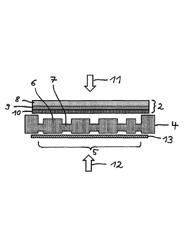
viewing in incident light;
9
CA 3008743 2019-07-25
Figure 3 the security-element region of the data carrier shown in Figure 1
upon the
viewing in transmitted light;
Figure 4 the security-element region of the data carrier shown in Figure 1
along the A-A'
line in cross-sectional view according to a first embodiment example;
Figure 5 the security-element region of the data carrier shown in Figure 1
along the A-A'
line in cross-sectional view according to a second embodiment example;
Figure 6 the schematic construction of a further data carrier according to an
embodiment
of the present disclosure which is equipped with a strip-shaped security
element; and
Figure 7 the security-element region of the data carrier shown in Figure 6
along the B-B'
line in cross-sectional view according to an embodiment example.
[0046] Fig. 1 shows the schematic construction of a data carrier according to
an
embodiment of the present disclosure, namely a bank note 1 which is equipped
with a
patch-shaped security element 2. In the present case the bank-note substrate
is a paper
substrate which has a lower thickness inside the dashed region 3 than outside
the dashed
region 3, i.e. it is thinned. Inside the thinned region 3, the bank-note
substrate
furthermore has a watermark, namely the numeral "50". The watermark is based
on
thinned paper regions and thickened paper regions.
[0047] The security element 2 has the following layers:
a) a transparent carrier substrate, namely polyethylene terephthalate (PET)
foil;
b) an emboss-lacquer layer which has a relief structure forming a diffractive
structure
and/or relief structure forming a micromirror arrangement;
c) a semi-transparent function layer, namely
c1) a first semi-transparent aluminum layer;
c2) an SiO2 layer;
c3) a second semi-transparent aluminum layer;
d) a heat-seal coating which is suitable for the bonding of the security
element with
the bank note substrate.
[0048] The layers c1), c2) and c) form a semi-transparent function layer which
upon the
viewing in incident light appears metallically gold-colored and bluish upon
the viewing
CA 3008743 2019-07-25
in transmitted light.
[0049] Figure 2 shows the security-element region 2 of the bank note 1 shown
in the
Figure 1 upon the viewing in transmitted light. The viewer perceives the
security-
element region 2 in the form of an opaque, gold-colored metallization.
[0050] Figure 3 shows the security-element region 2 of the bank note 1 shown
in the
Figure 1 upon the viewing in transmitted light. The viewer perceives the
security-
element region 2 in blue color, wherein the blue inside the dashed region 3 is
brighter
than in the edge region as a result of the thinned bank-note paper. Inside the
security-
element region 2, the viewer sees furthermore the watermark, namely the
numeral
50", in the form of contrast differences between dark blue and light blue.
[0051] Figure 4 shows the security-element region 2 of the bank note 1 shown
in Figure 1
along the A-A' line in cross-sectional view according to a first embodiment
example. The
reference number 5 designates the paper substrate which is thinned inside the
regions
designated with the bracket 5. In the thinned region 5, the paper substrate
furthermore
has thickened areas 6 and thinned areas 7 which together form the watermark
"50" in
Figure 1. The security element applied to the paper substrate 2 contains a
transparent
carrier substrate 8, an emboss-lacquer layer 9 and a semi-transparent function
layer 10.
The security element 2 has furthermore a heat-seal coating which is suitable
for the
bonding of the security element with the bank-note substrate (not shown in
Figure 4).
[0052] The reference number 13 represents an optionally present back-side foil
which is
applied for stabilizing the flatness of the bank note on the side of the bank-
note substrate
opposing the security element 2.
[0053] The block arrow 11 represents the view of the viewer onto the security
element
2 upon the viewing in transmitted light, namely against a light source
represented by
the block arrow 12.
[0054] Figure 5 shows the security-element region 2 of the bank note 1 shown
in Figure 1
along the A-A' line in cross-sectional view according to a second embodiment
example.
11
CA 3008743 2019-07-25
The reference number 14 designates the paper substrate which is thinned inside
the
regions designated with the bracket 15. In the thinned region 15, the paper
substrate 14
has furthermore paper regions printed with opaque color 16 and unprinted paper
regions 17 which together form the watermark "50" in Figure 1. The security
element
applied to the paper substrate 2 contains a transparent carrier substrate 8,
an emboss-
lacquer layer 9 and a semi-transparent function layer 10. The security element
2 has
furthermore a heat-seal coating which is suitable for the bonding of the
security element
with the bank-note substrate (not shown in Figure 5).
[0055] The block arrow 11 represents the view of the viewer onto the security
element
2 upon the viewing in transmitted light, namely against a light source
represented by
the block arrow 12.
[0056] The reference number 13 represents an optionally present back-side foil
which is
applied for stabilizing the flatness of the bank note on the side of the bank-
note substrate
opposing the security element 2.
[0057] Figure 6 shows the schematic construction of a further data carrier
according
to the present disclosure, namely a bank note 18, which is equipped with a
strip-
shaped security element 19.
[0058] In the present case, the bank-note substrate is a paper substrate which
has inside
the dashed region 20 a window region formed by an aperture or recess and has
inside
the dashed region 21 a lower thickness than outside the dashed region 21, i.e.
it is
thinned. Inside the thinned region 21 the bank-note substrate furthermore has
a
watermark, namely the numeral "50". The watermark is based on thinned paper
regions
and thickened paper regions.
[0059] The security element 19 has the following layers:
a) a transparent carrier substrate, namely polyethylene terephthalate (PET)
foil;
b) an emboss-lacquer layer which has, on the one hand, regions having a relief
structure
forming a diffractive structure and/or a micromirror arrangement and has, on
the other
hand, regions without relief structure;
12
CA 3008743 2019-07-25
c) a semi-transparent function layer, namely
c1) a first semi-transparent aluminum layer;
c2) an SiO2 layer;
c3) a second semi-transparent aluminum layer;
d) a heat-seal coating which is suitable for the bonding of the security
element with
the bank note substrate.
[0060] The layers c1), c2) and c) form a semi-transparent function layer which
upon the
viewing in incident light appears metallically gold-colored and bluish upon
the viewing
in transmitted light.
[0061] Figure 7 shows the security-element region of the data carrier shown in
Figure
6 along the B-B' line in cross-sectional view according to an embodiment
example.
[0062] The reference number 22 designates the paper substrate which is thinned
inside the
region designated with the bracket 23 and has a recess, i.e. a window region,
inside the
region designated with the bracket 24. In the thinned rcgion 23, the paper
substrate 22 has
furthermore thickened areas 25 and thinned areas 26 which together form the
watermark
"50" in Figure 6. The security element 19 applied to the paper substrate
contains a
transparent carrier substrate 27 and an emboss-lacquer layer 28 which has, on
the one
hand, regions 28a having a relief structure forming a diffractive structure
and/or a
micromirror arrangement and has, on the other hand, regions 28b without relief
structure. In addition, the security element 19 has in some areas a semi-
transparent
function layer 29. The security element 19 is furthermore equipped with a heat-
seal
coating which is suitable for the bonding of the security element 19 with the
bank-note
substrate 22 (not shown in Figure 7).
[0063] The reference number 30 represents an optionally present back-side foil
which is
applied for stabilizing the flatness of the bank note 18 on the side of the
bank-note
substrate 22 opposing the security element 19.
[0064] The block arrows 31 and 32 represent respectively the view of the
viewer
onto the security element 19 in the watermark region 23 or the window region
24.
13
CA 3008743 2019-07-25
[0065] The block arrow 33 represents a relatively strong light source which is
required
for the perceptibility of the watermarks formed by the numeral "50" upon the
viewing of
the bank note 18 in the region 23 in transmitted light.
[0066] The block arrow 34 represents a relatively weak light source which is
required for
the perceptibility of the motifs formed in the window region 24. The motif is
generated
by the semi-transparent function layer 29, which is adapted in the window
region 24 to
the emboss-lacquer layer region 28a having a relief structure. The relief
structure of the
emboss-lacquer layer continues in the semi-transparent function layer, so that
the viewer
perceives e.g. a micromirror arrangement in the window region 24.
14
CA 3008743 2019-07-25