Note: Descriptions are shown in the official language in which they were submitted.
METHODS AND APPARATUS FOR
FUNCTIONAL INSERT WITH POWER LAYER
This application is a divisional of Canadian Patent Application No. 2,830,983,
filed March 20, 2012.
RELATED APPLICATIONS
This application claims priority to U.S. Patent Application Serial No.
13/401,959
filed February 22, 2012; and U.S. Provisional Application Serial No.
61/454,591filed
March 21, 2011, entitled Methods and Apparatus for Functional Insert with
Power Layer.
FIELD OF USE
This invention describes a functionalized insert for logic processing device
formed
from multiple functional layers which are stacked, wherein at least one layer
includes a
power source as well as, in some embodiments, methods and apparatus for the
fabrication
of an ophthalmic lens with a functionalized insert of multiple stacked layers.
BACKGROUND
Traditionally an ophthalmic device, such as a contact lens, an intraocular
lens or a
punctal plug included a biocompatible device with a corrective, cosmetic or
therapeutic
quality. A contact lens, for example, may provide one or more of: vision
correcting
functionality; cosmetic enhancement; and therapeutic effects. Each function is
provided
by a physical characteristic of the lens. A design incorporating a refractive
quality into a
lens may provide a vision corrective function. A pigment incorporated into the
lens may
provide a cosmetic enhancement. An active agent incorporated into a lens may
provide a
therapeutic functionality. Such physical characteristics are accomplished
without the lens
entering into an energized state. A punctal plug has traditionally been a
passive device.
More recently, it has been theorized that active components may be
incorporated
into a contact lens. Some components may include semiconductor devices. Some
examples have shown semiconductor devices embedded in a contact lens placed
upon
animal eyes. It has also been described how the active components may be
energized and
activated in numerous manners within the lens structure itself. The topology
and size of
1
CA 3009920 2018-06-27
the space defined by the lens structure creates a novel and challenging
environment for the
definition of various functionality. Generally, such disclosures have included
discrete
devices. However, the size and power requirements for available discrete
devices are not
necessarily conducive for inclusion in a device to be worn on a human eye.
SUMMARY
Accordingly, the present invention includes designs of components that may be
combined to form a stacked layer of substrates combined into a discrete
package. The
stacked layers will include one or more layers which include a power source
for at least
one component included in the stacked layers. In some embodiments, an insert
is provided
that may be energized and incorporated into an ophthalmic device. The insert
may be
formed of multiple layers which may have unique functionality for each layer;
or
alternatively mixed functionality but in multiple layers. The layers may in
some
embodiments have layers dedicated to the energization of the product or the
activation of
the product or for control of functional components within the lens body. In
addition,
methods and apparatus for forming an ophthalmic lens, with inserts of stacked
functionalized layers are presented.
In some embodiments, the insert may contain a layer in an energized state
which is
capable of powering a component capable of drawing a current. Components may
include,
for example, one or more of: a variable optic lens element, and a
semiconductor device,
which may either be located in the stacked layer insert or otherwise connected
to it.
In another aspect, some embodiments may include a cast molded silicone
hydrogel
contact lens with a rigid or formable insert of stacked functionalized layers
contained
within the ophthalmic lens in a biocompatible fashion, wherein at least one of
the
functionalized lens includes a power source.
Accordingly, the present invention includes a disclosure of an ophthalmic lens
with
a stacked functionalized layer portion, apparatus for forming an ophthalmic
lens with a
stacked functionalized layer portion and methods for the same. An insert may
be formed
from multiple layers in various manners as discussed herein and the insert may
be placed
in proximity to one, or both of, a first mold part and a second mold part. A
reactive
monomer mix is placed between the first mold part and the second mold part.
The first
mold part is positioned proximate to the second mold part thereby forming a
lens cavity
with the energized substrate insert and at least some of the reactive monomer
mix in the
2
CA 3009920 2018-06-27
lens cavity; the reactive monomer mix is exposed to actinic radiation to form
an
ophthalmic lens. Lenses may be formed via the control of actinic radiation to
which the
reactive monomer mixture is exposed.
DESCRIPTION OF THE DRAWINGS
FIG. 1 illustrates a block diagram of some embodiments of a power source
layer.
FIG. 2 illustrates some exemplary embodiments of form factor for a wire based
power
source.
FIG. 3 illustrates a three dimensional representation of an insert formed of
stacked
functional layers which is incorporated within an ophthalmic lens mold part.
Fig. 4 illustrates a cross sectional representation of an ophthalmic lens mold
part with an
insert.
Fig. 5 demonstrates an exemplary embodiment of an insert comprising multiple
stacked
functional layers upon a supporting and aligning structure.
Fig. 6 illustrates different shapes and embodiments of the components used for
forming
layers in a stacked functional layer insert.
DETAILED DESCRIPTION OF THE INVENTION
The present invention includes a substrate insert device formed through the
stacking of multiple functionalized layers. Additionally the present invention
includes
methods and apparatus for manufacturing an ophthalmic lens with such a stacked
functionalized layer substrate as an insert in the formed lens. In addition,
some
embodiments of the present invention include an ophthalmic lens with a stacked
functionalized layer substrate insert incorporated into the ophthalmic lens.
In the following sections detailed descriptions of embodiments of the
invention
will be given. The description of both preferred and alternative embodiments
are
exemplary embodiments only, and it is understood that to those skilled in the
art that
variations, modifications and alterations may be apparent. It is therefore to
be understood
that said exemplary embodiments do not limit the scope of the underlying
invention.
GLOSSARY
In this description and claims directed to the presented invention, various
terms may
3
CA 3009920 2018-06-27
be used for which the following definitions will apply:
Energized: as used herein refers to the state of being able to supply
electrical
current to or to have electrical energy stored within.
Energy: as used herein refers to the capacity of a physical system to do work.
Many uses within this invention may relate to the said capacity being able to
perform
electrical actions in doing work.
Energy Source: as used herein refers to device or layer which is capable of
supplying Energy or placing a logical or electrical device in an Energized
state.
Energy Harvesters: as used herein refers to device capable of extracting
energy
from the environment and convert it to electrical energy.
Functionalized: as used herein refers to making a layer or device able to
perform a
function including for example, energization, activation, or control.
Lens: refers to any ophthalmic device that resides in or on the eye. These
devices
may provide optical correction or may be cosmetic. For example, the term lens
may refer
to a contact lens, intraocular lens, overlay lens, ocular insert, optical
insert or other similar
device through which vision is corrected or modified, or through which eye
physiology is
cosmetically enhanced (e.g. iris color) without impeding vision. In some
embodiments,
the preferred lenses of the invention are soft contact lenses are made from
silicone
elastomers or hydrogels, which include but are not limited to silicone
hydrogels, and
fluorohydrogels.
Lens forming mixture or "Reactive Mixture" or "RMM" (reactive monomer
mixture): as used herein refers to a monomer or prepolymer material which may
be cured
and crosslinked or crosslinked to form an ophthalmic lens. Various embodiments
may
include lens forming mixtures with one or more additives such as: UV blockers,
tints,
photoinitiators or catalysts, and other additives one might desire in an
ophthalmic lenses
such as, contact or intraocular lenses.
Lithium Ion Cell: refers to an electrochemical cell where Lithium ions move
through the cell to generate electrical energy. This electrochemical cell,
typically called a
battery, may be reenergized or recharged in its typical forms.
Substrate insert: as used herein refers to a formable or rigid substrate
capable of
supporting an Energy Source within an ophthalmic lens. In some embodiments,
the
Substrate insert also supports one or more components.
Mold: refers to a rigid or semi-rigid object that may be used to form lenses
from
uncured formulations. Some preferred molds include two mold parts forming a
front curve
4
CA 3009920 2018-06-27
mold part and a back curve mold part.
Optical Zone: as used herein refers to an area of an ophthalmic lens through
which
a wearer of the ophthalmic lens sees.
Power: as used herein refers to work done or energy transferred per unit of
time.
Rechargeable or Re-energizable: as used herein refers to a capability of being
restored to a state with higher capacity to do work. Many uses within this
invention may
relate to the capability of being restored with the ability to flow electrical
current at a
certain rate for a certain, reestablished time period.
Reenergize or Recharge: To restore to a state with higher capacity to do work.
Many uses within this invention may relate to restoring a device to the
capability to flow
electrical current at a certain rate for a certain, reestablished time period.
Released from a mold: means that a lens is either completely separated from
the
mold, or is only loosely attached so that it may be removed with mild
agitation or pushed
off with a swab.
Stacked: as used herein means to place at least two component layers in
proximity
to each other such that at least a portion of one surface of one of the layers
contacts a first
surface of a second layer. In some embodiments, a film, whether for adhesion
or other
functions may reside between the two layers that are in contact with each
other through
said film.
Description
Powered Layers
Referring now to Fig. 1, in some embodiments, one or more layers of a
functionalized stack of substrates may include a thin film electrical power
source 100. The
thin electrical power source may be viewed essentially as a battery on a
substrate.
A thin film battery (sometimes referred to as a TFB) may be structured on a
suitable substrate, such as silicon, using known deposition processes.
Deposition may
include, for example, sputter deposition and may be used to deposit various
materials
using one or more of masking and material removal techniques.
A wide variety of different materials have been studied and are possible. In
some
applications, such as for example, die stack and an ophthalmic device; a
preferable
substrate includes one that is able to withstand 800 deg. C without chemical
change. In
another aspect, a preferable substrate may be insulating. Optionally, the
substrate may
5
CA 3009920 2018-06-27
have vias that interconnect current collectors from a top side of the device
to a bottom
side.
A TFB according to the present invention will preferably be enclosed in a
packaging to prevent ingress of one or more of: oxygen, moisture other gasses
or liquids.
Preferred embodiments may therefore include packaging in one or more layers
wherein the
packaging may include one or more of an insulative (e.g. parylene) and
impermeable layer
(e.g. metals, aluminum, titanium, etc.) . Layers may be applied by deposition
over a TFB
device.
Preferably interconnects remain accessible to electrical communication outside
the
package. In some embodiments, electrical communication may include a
conductive path.
In other embodiments, electrical communication may include a wireless
transport of
energy, such as via a radio frequency or light wavelength.
Other methods include applying organic materials (e.g. epoxy) in conjunction
with
pre-shaped impermeable materials (e.g. the next layer of the die stack, or a
precision
formed /cut glass, alumina, or silicon cover layer.
Wire Formed Power Source
Referring now to Fig. 2A, an exemplary design of some embodiments of a power
source which includes a battery formed about a conductive wire. Preferably the
battery
will include a high aspect ratio wire battery.
In some embodiments, a fine gauge copper wire may be used as a support.
Various battery component layers may be built up using batch or continuous
wire coating
processes. In this manner, a very high volumetric efficiency (>60 %) of active
battery
materials can be achieved in a convenient form factor that is flexible. In
some
embodiments, a thin wire may be utilized to form small batteries, such as, for
example, a
battery in a range measured by Milliamp hours. Voltage capacities may be
targeted to be
approximately 1.5 volts, direct current. Larger batteries and higher voltages
may also be
scaled and are within the scope of the present invention.
Typically, a wire formed battery provides a significant improvement (-40x or
more) over an incumbent thin film 6-pack.
Referring now to Fig. 2B, a method is illustrated for forming some embodiments
of a wire based battery. A copper wire of high purity such as those available
from
commercial source, such as McMaster Carr Corp. may be used coated with one or
more
layers.
6
CA 3009920 2018-06-27
In some embodiments, a zinc anode coating may be formulated from zinc metal
powder, polymer binders, solvents, and additives. The coating may be applied
and
immediately dried. Multiple passes of the same coating may be used to achieve
the
desired thickness.
A separator coating may be formulated from non-conductive filler particles,
polymer binders, solvents, and additives. Application method may be the same.
A silver oxide cathode coating may be formulated from Ag20 powder, graphite,
polymer binders, solvents, and additives. Application method may be the same.
The wire battery may be coated with current collector (e.g. carbon conductive
adhesive, silver conductive adhesive, or the like).
Electrolyte (potassium hydroxide solution with additives) may be applied to
the
finished battery to complete construction.
The cell should remain "open" (i.e. non-hermetic) so as to allow any evolved
gases
to safely leave. Silicone or fluoropolymer coatings may be used to protect the
battery from
mechanical damage, and to contain liquid electrolyte within.
The battery may have an open circuit voltage of 1.5 V or greater.
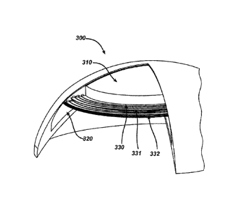
Referring now to Fig. 3 a three dimensional representation is illustrated of
some
embodiments of a fully formed ophthalmic lens using a stacked layer substrate
insert of the
time in item 210 is demonstrated as item 300. The representation shows a
partial cut out
from the ophthalmic lens to realize the different layers present inside the
device. Item 320
shows the body material in cross section of the encapsulating layers of the
substrate insert.
This item surrounds the entire periphery of the ophthalmic lens. It may be
clear to one
skilled in the arts that the actual insert may comprise a full annular ring or
other shapes
that still may reside within the constraints of the size of a typical
ophthalmic lens.
Items 330, 331 and 332 are meant to illustrate three of numerous layers that
may
be found in a substrate insert formed as a stack of functional layers. In some
embodiments, a single layer may include one or more of: active and passive
components
and portions with structural, electrical or physical properties conducive to a
particular
purpose.
In some embodiments, a layer 330 may include an energization source, such as,
for
example, one or more of: a battery, a capacitor and a receiver within the
layer 330. Item
331 then, in a non limiting exemplary sense may comprise microcircuitry in a
layer that
detects actuation signals for the ophthalmic lens. In some embodiments, a
power
regulation layer 332, may be included that is capable of receiving power from
external
7
CA 3009920 2018-06-27
sources, charges the battery layer 330 and controls the use of battery power
from layer
330 when the lens is not in a charging environment. The power regulation may
also
control signals to an exemplary active lens, demonstrated as item 310 in the
center annular
cutout of the substrate insert.
An energized lens with an embedded Substrate insert may include an Energy
Source, such as an electrochemical cell or battery as the storage means for
the energy and
in some embodiments, encapsulation and isolation of the materials comprising
the Energy
Source from an environment into which an ophthalmic lens is placed.
In some embodiments, a Substrate insert also includes a pattern of circuitry,
components and Energy Sources. Various embodiments may include the Substrate
insert
locating the pattern of circuitry, components and Energy Sources around a
periphery of an
optic zone through which a wearer of a lens would see, while other embodiments
may
include a pattern of circuitry, components and Energy Sources which are small
enough to
not adversely affect the sight of a contact lens wearer and therefore the
Substrate insert
may locate them within, or exterior to, an optical zone.
In general, according to these embodiments previously described, a Substrate
insert
111 is embodied within an ophthalmic lens via automation which places an
Energy Source
a desired location relative to a mold part used to fashion the lens.
Fig. 4 illustrates a closer view of some embodiments of a stacked functional
layer
insert 400 seen in cross section. Within the body of the ophthalmic lens 410
is embedded
the functionalized layer insert 420 which surrounds and connects to an active
lens
component 450, in some embodiments. It may be clear to one skilled in the
arts, that this
example shows but one of numerous embodiments of embedded function that may be
placed within an ophthalmic lens.
Within the stacked layer portion of the insert are demonstrated numerous
layers.
In some embodiments the layers may comprise multiple semiconductor based
layers. For
example, item 440, the bottom layer in the stack, may be a thinned silicon
layer upon
which circuits have been defined for various functions. Another thinned
silicon layer may
be found in the stack as item 441. In a non-limiting example, such a layer may
have the
function of energization of the device. These silicon layers will in some
embodiments be
electrically isolated from each other through an intervening insulator layer
show as item
450. The portions of the surface layers of items 440, 450 and 441 that overlap
each other
may be adhered to each other through the use of a thin film of adhesive. It
may be obvious
to one skilled in the arts that numerous adhesives may have the desired
characteristics to
8
CA 3009920 2018-06-27
adhere and passivate the thin silicon layers to the insulator, as in an
exemplary sense an
epoxy might.
A multiple stacked layer may include additional layers 442, which in an non
limiting example may include a thinned silicon layer with circuitry capable of
activating
and controlling an active lens component. As mentioned before, when the
stacked layers
need to be electrically isolated from each other, stacked insulator layers may
be included
between the electrically active layer and in this example item 451 may
represent this
insulator layer comprising part of the stacked layer insert. In some of the
examples
described herein, reference has been made to layers formed from thin layers of
silicon.
The general art may be extended to different embodiments where the material
definitions
of the thin stacked layers include, in a non limiting sense, other
semiconductors, metals or
composite layers. And the function of the thin layers may include electrical
circuitry, but
also may include other functions like signal reception, energy handling and
storage and
energy reception to mention a few examples. In embodiments with different
material
types, the choice of different adhesives, encapsulants and other materials
which interact
with the stacked layers may be required. In an example embodiment, a thin
layer of epoxy
may adhere three silicon layers shown as 440, 441 and 442 with two silicon
oxide layers
450 and 451.
As mentioned in some of the examples the thinned stacked layer may comprise
circuits formed into silicon layers. There may be numerous manners to
fabricate such
layers, however, standard and state of the art semiconductor processing
equipment may
form electronic circuits on silicon wafers using generic processing steps.
After the circuits
are formed into the appropriate locations on the silicon wafers, wafer
processing
equipment may be used to thin the wafers from hundreds of microns thick to
thicknesses
of 50 microns or less. After thinning the silicon circuits may be cut or
"diced" from the
wafer into the appropriate shapes for the ophthalmic lens or other
application. In later
section, different exemplary shapes of the stacked layer invention disclosed
herein are
shown in Fig. 6. These will be discussed in detail later; however, the
"dicing" operation
may use various technical options to cut out thin layers with curved,
circular, annular,
rectilinear and other more complicated shapes.
When the stacked layers perform a function relating to electrical current
flow, in
some embodiments, there may be a need to provide electrical contact between
the stacked
layers. In the general field of semiconductor packaging this electrical
connection between
stacked layers has generic solutions comprising wire bonding, solder bumping
and wire
9
CA 3009920 2018-06-27
deposition processes. Some embodiments of wire deposition may use printing
process
where electrically conductive inks are printed between two connection pads. In
other
embodiments, wires may be physically defined by an energy source, like for
example a
laser, interacting with a gaseous, liquid or solid chemical intermediate
resulting in an=
electrical connection where the energy source irradiates. Still further
interconnection
definition embodiments may derive from photolithographic processing before or
after
metal films are deposited by various means.
In the invention herein, if one or more of the layers needs to communicate
electrical signals outside itself, it may have a metal contact pad that is not
covered with
passivating and insulating layers. In many embodiments these pads would be
located on
the periphery of the layer where subsequent stacked layers do not cover the
region. In an
example of this type of embodiment, in Fig. 4 interconnect wires 430 and 431
are
demonstrated as electrically connecting peripheral regions of layers 440, 441
and 442. It
may be apparent to one skilled in the art that numerous layouts or designs of
where the
electrical connection pads are located and the manner of electrically
connecting various
pads together. Furthermore, it may be apparent that different circuit designs
may derive
from the choice of which electrical connect pads are connected and to which
other pads
they are connected. Still further, the function of the wire interconnection
between pads
may be different in different embodiments including the functions of
electrical signal
connection, electrical signal reception from external sources, electrical
power connection
and mechanical stabilization to mention a few examples.
In a previous discussion, it was presented that non semiconductor layers may
comprise one or more of the stacked layers in the inventive art. It may be
apparent that
there could be a great diversity of applications which may derive from
nonsemiconductor
layers. In some embodiments, the layers may define energizing sources like
batteries.
This type of layer in some cases may have a semiconductor acting as the
supporting
substrate for the chemical layers, or in other embodiments may have metallic
or insulating
substrates. Other layers may derive from layers which are primarily metallic
in nature.
These layers may define antennas, thermal conductive paths, or other
functions. There
may be numerous combinations of semiconducting and non semiconducting layers
that
comprise useful application within the spirit of the inventive art herein.
In some embodiments where electrical connection is made between stacked layers
the electrical connection will need to be sealed after connection is defined.
There are
numerous methods that may be consistent with the art herein. For example, the
epoxy or
CA 3009920 2018-06-27
other adherent materials used to hold the various stacked layers together
could be reapplied
to the regions with electrical interconnect. Additionally, passivation films
may, in some
embodiments, be deposited across the entire device to encapsulate the regions
that were
used for interconnection. It may be apparent to one skilled in the art that
numerous
encapsulating and sealing schemes may be useful within this art to protect,
strengthen and
seal the stacked layer device and its interconnections and interconnection
regions.
Assembling Stacked Functionalized Layer Inserts
Proceeding to Fig. 5, item 500, a close up view of an exemplary apparatus to
assemble stacked functionalized layer inserts is demonstrated. In the example,
a stacking
technique where the stacked layers do not align on either side of the layer is
shown. Items
440, 441 and 442 again may be silicon layers. On the right side of the Fig. it
may be seen
that the right side edge of the items 440, 441 and 442 do not align with each
other, as they
may in alternative embodiments. Such a stacking methodology may allow the
insert to
assume a three dimensional shape similar to that of the general profile of an
ophthalmic
lens. In some embodiments as well, such a stacking technique may allow for the
layers to
be made from the largest surface area as possible. In layers that are
functional for energy
storage and circuitry such surface area maximization may be important.
In general many of the features of the previously described stacked inserts
may be
observed in Fig. 5 including stacked functional layers 440, 441 and 442;
stacked
insulating layers 450 and 451; and interconnections 430 and 431. Additionally
a
supporting jig, item 510, may be observed to support the stacked
functionalized layer
insert as it is being assembled. It may be apparent that the surface profile
of item 510 may
assume a large number of shapes which will change the three dimensional shape
of inserts
made thereon.
In general, a jig 510 may be provided with a predetermined shape. It may be
coated with different layers, item 520, for a number of purposes. In a non
limiting
exemplary sense, the coating may first comprise a polymer layer that will
allow easy
incorporation of an insert into the base material of an ophthalmic lens, and
may even be
formed from a polysilicone material in some embodiments. An epoxy coating may
then be
deposited upon the polysilicone coating to adhere the bottom thin functional
layer 440 to
the coating 520. The bottom surface of a next insulating layer 450 may then be
coated
with a similar epoxy coating and then placed into its appropriate location
upon the jig. It
may be clear that the jig may in some embodiments have the function of
aligning the
correct placement of the stacked layers relative to each other as the device
is assembled.
11
CA 3009920 2018-06-27
In repetitious fashion, the rest of the insert may then be assembled, the
interconnections
defined and then the insert encapsulated. In some embodiments, the
encapsulated insert
may then be coated from the top with a polysilicone coating. In some
embodiments that
use a polysilicone coating for item 520, the assembled insert may be
dissociated from the
jig 510 by hydration of the polysilicone coating.
The jig 510 may be formed from numerous materials. In some embodiments, the
jig may be formed and made of similar materials that are used to make molding
pieces in
the manufacture of standard contact lenses. Such a use could support the
flexible
formation of various jig types for different insert shapes and designs. In
other
embodiments the jig may be formed from materials that either in their own
right or with
special coatings will not adhere to the chemical mixtures used to adhere the
different
layers to each other. It may be apparent that numerous options may exist for
the
configuration of such a jig.
Another aspect of the jig demonstrated as item 510 is the fact that its shape
physically supports the layers upon it. In some embodiments the
interconnection between
the layers may be formed by wirebonding connection. In the process of
wirebonding
significant force is applied the wire to ensure it forms a good bond.
Structural support of
the layers during such bonding could be important and could be performed by
the
supporting jig 510.
Still another function of the jig demonstrated as item 510 is that the jig may
have
alignment features on it that allow for the alignment of pieces of the
functionalized layers
to be aligned both relative to each other linearly and radially along the
surfaces. In some
embodiments, the jig may allow the alignment of azimutal angle of the
functional layers
relative to each other around a center point. Regardless of the ultimate shape
of the insert
produced it may be apparent that the assembly jib may be useful in insuring
that the pieces
of the insert are properly aligned for their function and correct
interconnection.
Proceeding to Fig. 6, a more generalized discussion of shapes of stacked layer
inserts may be had. In a subset of the generality of shapes consistent with
the art, some
sample variation in shape is shown. For example, item 610 shows a top view of
a stacked
insert which has been formed from essentially circular layer pieces. In some
embodiments, the region shown with cross hatching 611 may be an annular region
where
layer material has been removed. However, in other embodiments, it may be
apparent that
the pieces of the stacked layers used form the insert could be disks without
an annular
region. Although, such a non annular insert shape may be of limited utility in
an
12
CA 3009920 2018-06-27
ophthalmic application the spirit of the inventive art herein is not intended
to be limited by
the presence of an internal annulus.
Item 620 may in some embodiments demonstrate different embodiments of a
stacked functional layer insert. As shown in item 621, in some embodiments the
layer
pieces may be discrete not only in the stacking direction but also around the
azimuthal
direction perpendicular to the stacking direction. In some embodiments,
semicircular
pieces may be used to form the insert. It may be apparent that in shapes that
have an
annular region, which partial shapes could be useful to reduce the amount of
material that
would need to be "diced" or cut out after the layer material is formed into
its function.
Proceeding further, item 630 demonstrates that non radial, non elliptical and
non
circular insert shapes could be defined. As shown in item 630, rectilinear
shapes may be
formed, or as in item 640 other polygonal shapes. In a three dimensional
perspective
pyramids, cones and other geometrical shapes could result from the different
shapes of the
individual layer pieces used to form the insert. In a more general sense it
may be apparent
to one skilled in the arts that a vast diversity of shapes may be formed into
shapes and
products to make o discuss the more general case of shapes that may be made
with the
functionality, energization, activation etc...
Conclusion
The present invention, as described above and as further defined by the claims
below, provides devices and methods for stacked functional layer inserts and
apparatus for
implementing such methods, as well as ophthalmic lenses formed including the
stacked
layers.
13
CA 3009920 2018-06-27