Note: Descriptions are shown in the official language in which they were submitted.
= 84350256
BIDIRECTIONAL OPTICAL SUB ASSEMBLY
TECHNICAL FIELD
[0001] The present invention relates to the field of optical
communications, and more
specifically, to a bidirectional optical sub assembly.
BACKGROUND
[0002] With overall popularization of optical networks, access
networks represented by
fiber to the home (Fiber To The Home, FTTH) are being deployed on a large
scale. Most
optical communications networks used for access are in a form of a passive
optical network
(Passive Optical Network, PON). Deployment of a large quantity of passive
optical networks
requires a huge quantity of optical communications devices, and therefore
there is an
increasing requirement for reducing optical communications device costs. A
related optical
communications device in an optical communications network mainly includes an
optical
module, and a most important component in the optical module is a
bidirectional optical sub
assembly (Bi-directional Optical sub-assembly, BOSA). Therefore, optical
communications
device cost reduction mainly depends on bidirectional optical sub assembly
cost reduction.
[0003] Currently, in the industry, a laser diode (Laser diode, LD)
that sends an optical
signal, a photodiode (Photodiode, PD) that receives an optical signal, and
another component
are generally packaged on one base, so as to reduce component costs. However,
because the
LD and the PD are located in same space, an optical signal sent by the LD is
received by the
PD, affecting receiving performance of the PD (that is, optical crosstalk of
the LD to the PD
occurs). In addition, because the LD converts an electrical signal into an
optical signal,
electromagnetic radiation generated by a high speed electrical signal spreads
around, and as a
result, the PD is interfered with, and the receiving performance of the PD is
affected (that is,
electrical crosstalk of the LD to the PD occurs).
[0004] In the prior art, to resolve a problem of optical and electrical
crosstalk of an LD to
1
CA 3010136 2018-07-10
84350256
a PD, a metal cover is added to cover an entire receiving area. There is an
opening on the
metal cover, so that both light transmission and electromagnetic shielding can
be
implemented.
[0005] However, space in the bidirectional optical sub assembly is very
small. To dispose
a shielding can, it is necessary to increase a size for packaging. In
addition, because the base
is a good conductor, electromagnetic radiation is transmitted on the base, and
electromagnetic
interference is caused to the PD that is disposed on the base. Consequently,
an anti-crosstalk
effect is unsatisfactory.
SUMMARY
[0006] Embodiments of the present invention provide a bidirectional optical
sub assembly,
to reduce optical and electrical crosstalk between a receiver and a
transmitter in the
bidirectional optical sub assembly.
[0007] According to a first aspect, a bidirectional optical sub assembly
is provided. The
bidirectional optical sub assembly includes: a base, a receiver, a
transmitter, a wavelength
division multiplexing part, an isolation part, an input port, and an output
port. The base is
made of a conducting material, and includes a first part and a second part,
there is a height
deviation H between the first part and the second part, and the height
deviation H is
determined according to relative positions of the receiver, the transmitter,
and the wavelength
division multiplexing part, where H is a positive number. The wavelength
division
multiplexing part is configured on the first part, and is configured to:
reflect an optical signal
of a first wavelength, or transmit an optical signal of a second wavelength,
where the first
wavelength is different from the second wavelength. The input port is
configured to transmit a
first electrical signal to the transmitter. The transmitter is configured to:
convert the first
electrical signal into a first optical signal, and transmit the first optical
signal to the
wavelength division multiplexing part. The wavelength division multiplexing
part is
configured to reflect the first optical signal. The wavelength division
multiplexing part is
further configured to transmit a second optical signal to the receiver. The
receiver is
configured to: receive the second optical signal, convert the second optical
signal into a
second electrical signal, and output the second electrical signal by using the
output port. The
2
CA 3010136 2018-07-10
84350256
isolation part is configured to electromagnetically isolate the receiver from
the transmitter.
[0008] With reference to the first aspect, in a first implementation of
the first aspect, the
wavelength division multiplexing part is a right-angle prism; a first right-
angle surface of the
right-angle prism is in contact with the first part surface to surface, a
through hole is disposed
on a surface, of the first right-angle surface, in contact with the first
part, and the through hole
is configured to make the second optical signal, that is transmitted through
the right-angle
prism, enter the second part and then be received by the receiver; an optical
film is plated on a
slope of the right-angle prism, and the optical film is used to reflect the
first optical signal or
transmit the second optical signal; and a photoresist adhesive is plated on a
surface other than
the slope and the first right-angle surface of the right-angle prism, and the
photoresist
adhesive is used to prevent stray light other than the second optical signal
from entering the
second part and being received by the receiver.
[0009] With reference to the first aspect and the foregoing
implementation of the first
aspect, in a second implementation of the first aspect, the bidirectional
optical sub assembly
further includes a trans-impedance amplifier and a ground cable pin, where the
trans-impedance amplifier is grounded by using the ground cable pin, and the
ground cable
pin is made of a conducting material, and is insulated from the base.
[0010] With reference to the first aspect and the foregoing
implementations of the first
aspect, in a third implementation of the first aspect, the bidirectional
optical sub assembly
further includes: a support part, made of a conducting material and configured
to support the
isolation part.
[0011] With reference to the first aspect and the foregoing
implementations of the first
aspect, in a fourth implementation of the first aspect, the second part is a
groove structure, the
isolation part is a metal sheet, and the metal sheet covers the groove.
[0012] With reference to the first aspect and the foregoing implementations
of the first
aspect, in a fifth implementation of the first aspect, at least one
independent pin is configured
on the base, and the at least one independent pin is insulated from the base.
[0013] With reference to the first aspect and the foregoing
implementations of the first
aspect, in a sixth implementation of the first aspect, the isolation part is
conductively
connected to the base.
[0014] With reference to the first aspect and the foregoing
implementations of the first
3
CA 3010136 2018-07-10
84350256
aspect, in a seventh implementation of the first aspect, a groove is
configured on the first part,
and an end, of the input port, that is used to connect to the transmitter is
disposed in the
groove.
[0015] According to the bidirectional optical sub assembly provided in
the embodiments
of the present invention, the base is divided into two spatially isolated
parts by using the
isolation part, and the receiver and the transmitter are respectively disposed
on the two parts
that are isolated from each other, so that the receiver is electromagnetically
isolated from the
transmitter, and optical and electrical crosstalk between the receiver and the
transmitter can be
eliminated.
BRIEF DESCRIPTION OF DRAWINGS
[0016] To describe the technical solutions in the embodiments of the
present invention
more clearly, the following briefly describes the accompanying drawings
required for
describing the embodiments or the prior art. Apparently, the accompanying
drawings in the
following description show merely some embodiments of the present invention,
and persons
of ordinary skill in the art may still derive other drawings from these
accompanying drawings
without creative efforts.
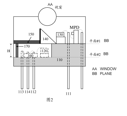
[0017] FIG 1 is a schematic structural diagram of a single-TO BOSA in
the prior art;
[0018] FIG 2 is a schematic structural diagram of a bidirectional
optical sub assembly
according to an embodiment of the present invention;
[0019] FIG 3 is a schematic top view of a bidirectional optical sub
assembly according to
an embodiment of the present invention;
[0020] FIG 4 is a schematic structural diagram of a bidirectional
optical sub assembly
according to another embodiment of the present invention;
[0021] FIG 5 is a schematic top view of a bidirectional optical sub
assembly according to
another embodiment of the present invention;
[0022] FIG. 6 is a schematic structural diagram of a bidirectional
optical sub assembly
according to still another embodiment of the present invention; and
[0023] FIG 7 is a schematic top view of a bidirectional optical sub
assembly according to
still another embodiment of the present invention.
4
CA 3010136 2018-07-10
84350256
[0024] Reference signs in the accompanying drawings:
110-base
111-input port
112-output port
113-ground cable pin
114-independent pin
120-receiver
130-transmitter
140-wavelength division multiplexing part
150-isolation part
160-trans-impedance amplifier
170-support part
DESCRIPTION OF EMBODIMENTS
[0025] A plurality of embodiments are now described with reference to
the accompanying
drawings, and same components in this specification are indicated by a same
reference
numeral. In the following description, for ease of explanation, many specific
details are
provided to facilitate comprehensive understanding of one or more embodiments.
However,
apparently, the embodiments may be not implemented by using these specific
details. In other
examples, a well-known structure and device are shown in a form of block
diagrams, to
conveniently describe one or more embodiments.
[0026] The following clearly and completely describes the technical
solutions in the
embodiments of the present invention with reference to the accompanying
drawings in the
embodiments of the present invention. Apparently, the described embodiments
are some but
not all of the embodiments of the present invention. All other embodiments
obtained by
persons of ordinary skill in the art based on the embodiments of the present
invention without
creative efforts shall fall within the protection scope of the present
invention.
[0027] It should be understood that technical solutions in the
embodiments of the present
invention may be applied to various optical networks, for example, a passive
optical network
(Passive Optical Network, PON). For ease of description, the PON is used as an
example
5
CA 3010136 2018-07-10
.84350256
instead of a limitation, to describe a bidirectional optical sub assembly in
the embodiments of
the present invention below.
[0028] In the prior art, to reduce costs of the bidirectional optical
sub assembly, an LD and
a PD are packaged on a same base, that is, the LD and the PD are located in
same enclosed
space. The LD converts an electrical signal into an optical signal, and the PD
converts an
optical signal into an electrical signal. If the LD is not photoelectrically
isolated from the PD,
the transmitter causes interference of optical crosstalk and electrical
crosstalk to the receiver.
On one hand an optical signal transmitted by a transmitter may reach a
receiver; or even if a
wavelength division multiplexing (Wavelength Division Multiplexing, WDM) part
is used to
isolate light transmitted by the LD from light to be received by the PD, due
to optical path
divergence, undetermined stray light exists and experiences reflection or
another operation
performed by surrounding components, and then reaches the PD in a zigzag
manner. Further,
an optical signal to be received by the PD is very weak compared with an
optical signal
transmitted by the LD. As a result, receiving performance of the PD is
affected. This is optical
crosstalk of the LD to the PD. On the other hand, because the LD converts the
electrical signal
into the optical signal, a high speed electrical signal is accompanied with
electromagnetic
radiation, that is, a signal to be converted by using the LD spreads around in
a form of
electromagnetic radiation. As a result, interference is caused to the PD and
an electronic
component behind the PD, and receiving performance is also affected. This is
electrical
crosstalk of the LD to the PD.
[0029] Currently, to eliminate optical and electrical crosstalk of the
transmitter to the
receiver in the bidirectional optical sub assembly, a solution is provided. In
this solution, a
receiving component and a transmitting component are disposed on a same base,
a
micro-feature platform made of a silicon (Si) material is used, and a PD is
spatially isolated
from an LD by using a platform feature, so that stray light from the LD can
hardly reach the
PD, or cause interference to the PD, thereby reducing optical crosstalk to
some extent.
However, features of this structure are complicated, and required components
need to be
customized. In addition, for electromagnetic radiation, the silicon material
cannot provide a
very good electromagnetic isolation effect. Further, costs are increased in
order to reduce the
optical and electrical crosstalk.
[0030] FIG 1 shows a schematic structural diagram of a single-TO BOSA in
another
6
CA 3010136 2018-07-10
84350256
solution. As shown in FIG 1, in this solution, a metal cover is added, to
cover an entire
receiving area. In this way, a receiver (or a PD) is enclosed in the metal
cover, and a
transmitter (or an LD) is outside the metal cover. In addition, there is an
opening on the metal
cover, and a WDM chip is disposed on the opening, so that light that is
incident through a
window is transmitted into the metal cover by the WDM chip, and then is
received by the PD.
Light transmitted by the LD may reach the WDM chip, and is transmitted through
the window
after being reflected by the WDM chip. Therefore, a metal cover structure is
disposed to
implement both light transmission and electromagnetic shielding.
[0031] However, space inside a transistor outline (Transistor Outline,
TO) is very small.
To dispose a shielding can, it is necessary to increase a size of the base for
packaging. In
addition, because the entire base is a good conductor, electromagnetic
radiation is transmitted
on the base, and electromagnetic interference is caused to the PD and a
related receiving
component that are disposed on the base. Consequently, an effect of optical
and electrical
crosstalk defense is unsatisfactory.
[0032] The following describes in detail a bidirectional optical sub
assembly according to
embodiments of the present invention with reference to FIG 2 to FIG. 5.
[0033] FIG 2 is a schematic structural diagram of a bidirectional
optical sub assembly
according to an embodiment of the present invention.
[0034] FIG. 3 shows a schematic top view of the bidirectional optical
sub assembly shown
in FIG 2.
[0035] As shown in FIG 2 and FIG 3, the bidirectional optical sub
assembly includes:
a base 110, a receiver 120, a transmitter 130, a wavelength division
multiplexing
part 140, an isolation part 150, an input port 111, and an output port 112.
[0036] The base 110 is made of a conducting material, and includes a
first part and a
second part.
[0037] The input port 111 and the output port 112 are respectively
configured to input an
electrical signal and output an electrical signal.
[0038] The receiver 120 is configured to perform optical-to-electrical
conversion.
[0039] The transmitter 130 is configured to perform electrical-to-
optical conversion.
[0040] The wavelength division multiplexing part 140 is configured to:
reflect an optical
signal of a first wavelength, or transmit an optical signal of a second
wavelength, where the
7
CA 3010136 2018-07-10
, 84350256
first wavelength is different from the second wavelength.
[0041] The isolation part 150 is configured to electromagnetically
isolate the receiver 120
from the transmitter 130.
[0042] The following separately describes in detail a connection
relationship, a structure,
and a function of each component with reference to FIG 2 and FIG. 3.
[0043] A. Base 110
[0044] The base 110 is used as a bearer component of a plurality of
components that are
included in the bidirectional optical sub assembly according to this
embodiment of the present
invention, and is made of a conducting material, for example, a conductor or a
semiconductor.
Further, in this embodiment of the present invention, as an example instead of
a limitation, the
base may be fabricated as a structure including two planes (that is, examples
of the first part
and the second part), for example, a plane #1 and a plane #2. As shown in FIG
2, another
component in this embodiment of the present invention may be separately
configured on the
plane #1 and the plane #2, and the receiver 120 and the transmitter 130 need
to be located on
different planes. In addition, there is a height deviation H between the plane
#1 and the plane
#2, H is a positive number, the height deviation H is determined according to
relative
positions of the receiver 120, the transmitter 130, and the wavelength
division multiplexing
part 140, and the height deviation H is a real number greater than zero. FIG 2
is used as an
example. The receiver 120 is configured on the plane #2. Therefore, the height
deviation H at
least ensures that the entire receiver 120 is disposed on the plane #2, and a
top of the receiver
to be still lower than the plane #1. It should be noted that in this
embodiment of the present
invention, the receiver 120 is used as an example to describe a condition that
the height
deviation H between the first part and the second part of the base 110 needs
to meet. However,
the present invention is not limited thereto. For example, when another
functional component
is configured on the plane #1, the condition should be determined by the
receiver and the
another functional component, so that all components can be totally disposed
on the plane #2,
and a peak of each component is not higher than the plane #1.
[0045] B. Receiver 120
[0046] The receiver 120 serves as a receiving component of an optical
signal, is
configured on the second part of the base 110, and is mainly configured to
implement a
function of optical-to-electrical conversion, so that a received optical
signal is converted into
8
CA 3010136 2018-07-10
84350256
an electrical signal. The receiver 120 may be a photoelectric sensor
component, for example,
may be a photodiode (Photodiode, PD).
[0047] C. Transmitter 130
[0048] The transmitter 130 is configured on the first part of the base
110, and is mainly
configured to implement a function of electrical-to-optical conversion, so
that an electrical
signal is converted into an optical signal. The transmitter 130 may be a laser
diode (Laser
diode, LD).
[0049] D. Wavelength division multiplexing part 140
[0050] In this embodiment of the present invention, the wavelength
division multiplexing
part 140 is mainly configured to process an optical signal according to a
wavelength of the
optical signal. The wavelength division multiplexing part 140 reflects the
optical signal of the
first wavelength; and the wavelength division multiplexing part 140 transmits
the optical
signal of the second wavelength, where the first wavelength is different from
the second
wavelength.
[0051] It should be noted that in this embodiment of the present invention,
serial numbers
"first" and "second" are merely used for distinguishing different objects such
as optical signals
of different wavelengths, and are not intended to limit the scope of this
embodiment of the
present invention.
[0052] E. Isolation part 150
[0053] The isolation part 150 is made of a conducting material, and the
isolation part 150,
the wavelength division multiplexing part 140, a plane (for example, the plane
#2 in FIG 2)
on which the second part of the base 110 is located, and a side wall (not
shown in the figure)
of the base 110 form a cavity, to enclose the receiver 120 configured on the
second part in the
cavity, so that electromagnetic interference between the receiver 120 and the
transmitter 130
.. that is configured on the plane #1 on which the first part of the base 110
is located can be
blocked. In this way, the receiver is electromagnetically isolated from the
transmitter.
[0054] Optionally, the wavelength division multiplexing part 140 is a
right-angle prism.
[0055] A first right-angle surface of the right-angle prism is in
contact with the first part
surface to surface, a through hole is disposed on a surface, of the first
right-angle surface, in
contact with the first part, and the through hole is configured to make a
second optical signal,
that is transmitted through the right-angle prism, enter the second part and
then be received by
9
CA 3010136 2018-07-10
. 84350256
the receiver 120.
[0056] An optical film is plated on a slope of the right-angle prism,
and the optical film is
used to reflect a first optical signal or transmit the second optical signal.
[0057] A photoresist adhesive is plated on a surface other than the
slope and the first
right-angle surface of the right-angle prism, and the photoresist adhesive is
used to prevent
stray light other than the second optical signal from entering the second part
and being
received by the receiver 120.
[0058] In this embodiment of the present invention, a wavelength is
selected by plating a
film on the surface of the right-angle prism, so that the right-angle prism
reflects the first
optical signal that is transmitted by the transmitter 130, and the first
optical signal is
transmitted outside through a window (shown in FIG 2). In addition, the right-
angle prism can
transmit the second optical signal that is incident through the window, so
that the second
optical signal enters the second part of the base 110 through the right-angle
prism, and is
received by the receiver 120 that is configured on the second part.
[0059] Specifically, the optical film is plated on the slope of the right-
angle prism, and the
optical film is used to reflect light of the first wavelength, and transmit
light of the second
wavelength. In addition, a photoresist adhesive is plated on the other three
surfaces except the
first right-angle surface (that is, a right-angle surface that is in contact
with the first part of the
base 110) of the right-angle prism, and the photoresist adhesive covers the
surfaces of the
right-angle prism, thereby reducing a possibility that an optical signal
transmitted by the
transmitter 130 enters the second part of the base 110 and is received by the
receiver 120.
[0060] It should be noted that in this embodiment of the present
invention, the right-angle
prism may be a 45-degree right-angle prism. This is not limited in this
embodiment of the
present invention.
[0061] Optionally, the bidirectional optical sub assembly further includes a
trans-impedance amplifier 160 and a ground cable pin 113.
[0062] The trans-impedance amplifier 160 is grounded by using the ground
cable pin 113,
the ground cable pin 113 is made of a conducting material, and is insulated
from the base 110.
[0063] Specifically, because light received by the receiver (for
example, the PD) 120 is
usually relatively weak, an electrical signal that is obtained after optical-
to-electrical
conversion by the receiver 120 is also weak, and generally needs to be
amplified for
CA 3010136 2018-07-10
84350256
processing. The trans-impedance amplifier (Trans-impedance amplifier, TIA) 160
is
configured to amplify the weak electrical signal that is output by the
receiver 120. Therefore,
the trans-impedance amplifier 160 is also configured on the second part of the
base 110, and is
electrically connected to the receiver 120. In addition, the ground cable pin
is configured on
.. the base 110, and the ground cable pin is insulated from the base 110. A
ground cable
electrode (not marked in the accompanying drawing) is configured on the trans-
impedance
amplifier, and the ground cable electrode is electrically connected to the
ground cable pin 113,
so that the trans-impedance amplifier is grounded.
[0064] It should be noted that in the prior art, the trans-impedance
amplifier 160 is
grounded by electrically connecting the trans-impedance amplifier to the base
110. It should
be understood that the base is made of a conducting material, and therefore,
electromagnetic
radiation may be transmitted on the base 110, an electromagnetic wave
transmitted on the
base 110 may cause electromagnetic interference to the receiver 120 configured
on the base
110, and performance of the receiver 120 for receiving a signal is affected.
In this embodiment
of the present invention, the ground cable pin 113 is configured on the base
110, the ground
cable pin 113 is insulated from the base 110, and the trans-impedance
amplifier is grounded
by using the ground cable pin 113, so that electrical crosstalk that is caused
to the receiver 120
by the electromagnetic wave generated on the base 110 can be reduced.
[0065] Optionally, the bidirectional optical sub assembly further
includes a support part
170, and the support part 170 is made of a conducting material, and is
configured to support
the isolation part 150.
[0066] It should be understood that in this embodiment of the present
invention, the base
110 includes the first part and the second part. When the second part is an
entire surface of the
base, the support part 170 needs to be configured, to support the isolation
part 150, so that the
isolation part 150, the first part of the base 110, the wavelength division
multiplexing part 140,
and the side wall of the base 110 form the cavity, and the first part is
spatially isolated from
the second part.
[0067] FIG 4 shows a schematic structural diagram of a bidirectional
optical sub
assembly according to another embodiment of the present invention.
[0068] FIG 5 shows a schematic top view of the bidirectional optical sub
assembly shown
in FIG. 4.
11
CA 3010136 2018-07-10
84350256
. .
[0069] Optionally, the second part is a groove structure, the
isolation part is a metal sheet,
and the metal sheet covers the groove.
[0070] As shown in FIG 4, a groove (that is, an example of the second
part) is disposed
on the base 110. In this case, the isolation part 150 may be a metal sheet,
and the metal sheet
covers the groove (for example, a groove 1 in FIG. 4), so as to eliminate
electrical crosstalk
that is caused to the receiver 120 by the base 110. That is, the metal sheet
and the groove
structure of the base are combined to form an electromagnetic crosstalk
shielding structure, so
as to eliminate electromagnetic interference in space.
[0071] Optionally, at least one independent pin 114 is configured on
the base 110, and the
at least one independent pin 114 is insulated from the base 110.
[0072] In the prior art, an electrode (for example, a ground cable
electrode) on the
trans-impedance amplifier 160 is connected to the base 110 by using a gold
wire, and the base
110 is made of a conducting material. Therefore, electromagnetic radiation is
transmitted on
the base. Consequently, electromagnetic interference is caused to the trans-
impedance
amplifier disposed on the base 110, and an anti-crosstalk effect is
unsatisfactory.
[0073] In this embodiment of the present invention, at least one
independent pin (for
example, the pin 114 in FIG 4) is configured on and insulated from the base
110, and is
configured to connect to at least one corresponding electrode on the trans-
impedance
amplifier 160, so that electromagnetic interference that is caused to the
trans-impedance
amplifier by the electromagnetic radiation transmitted on the base 110 can be
reduced without
increasing costs.
[0074] Optionally, the isolation part 150 is conductively connected to
the base 110.
[0075] Specifically, the isolation part 150 may be conductively
connected to the base 110
by using laser welding and the like. In this way, the isolation part 150 and
the base 110 may
properly form a shielding can, to block electromagnetic radiation in space, so
that
anti-electrical crosstalk performance of the bidirectional optical sub
assembly can be
improved.
[0076] FIG 6 is a schematic structural diagram of a bidirectional
optical sub assembly
according to still another embodiment of the present invention.
[0077] FIG 7 is a schematic top view of the bidirectional optical sub
assembly according
to still another embodiment of the present invention.
12
CA 3010136 2018-07-10
. 84350256
[0078] Optionally, a groove is configured on the first part, and an end,
of the input port
111, that is used to connect to the transmitter 130 is disposed in the groove.
100791 As shown in FIG 6 and FIG 7, a plane #3 is a plane on which the
base 110 is
located, and a groove (for example, a groove 2 in FIG 6) is configured on the
first part of the
base 110. The end, of the input port 111, that is used to connect to the
transmitter 130 (refer to
an end, of the input port 111, that is wired to the transmitter 130 in FIG 6)
is disposed in the
groove. Because the input port 111 is made of a conducting material, an
electromagnetic wave
generated by an electrical signal that is input from the input port 111 is
radiated around. A
groove structure in this embodiment of the present invention can block
electromagnetic
radiation. In this way, electrical crosstalk of the input port 111 to the PD
can be reduced.
[0080] It should be noted that in this embodiment of the present
invention, the end, of the
input port 111, that is used to connect to the transmitter 130 may be disposed
in the groove, or
the transmitter 130 or an entire transmission area may be disposed in the
groove. This is not
limited in this embodiment of the present invention.
[0081] In addition, a monitor photodiode (Monitor Photodiode, MPD) shown in
FIG 2,
FIG. 4, and FIG. 6 is configured to monitor a working status of the LD. This
is not described
in detail in this embodiment of the present invention.
[0082] The foregoing describes a structure of the bidirectional optical
sub assembly
according to the embodiment of the present invention with reference to FIG 2
to FIG 7. The
.. following uses FIG 2 as an example, to separately describe processes of
signal receiving (that
is, a case 1) and signal transmitting (that is, a case 2) by the bidirectional
optical sub assembly
according to the embodiments of the present invention.
[0083] Case 1
[0084] First, an electrical signal (denoted as an electrical signal 1
below) that requires
electrical-to-optical conversion is input to the bidirectional optical sub
assembly by using the
input port 111, and the input port 111 transmits the first electrical signal
to the transmitter 130.
The transmitter 130 performs electrical-to-optical conversion on the
electrical signal 1, and
converts the electrical signal 1 into an optical signal (denoted as an optical
signal 1 below).
The optical signal 1 generated by the transmitter 130 is transmitted to the
wavelength division
multiplexing part 140, and more precisely, the optical signal 1 is transmitted
to a slope of the
wavelength division multiplexing part 140. The wavelength division
multiplexing part 140
13
CA 3010136 2018-07-10
. 84350256
reflects the incident optical signal, and then optical signal is transmitted
outside through a
window. In this way, the bidirectional optical sub assembly completes optical
signal
transmission.
[0085] Case 2
[0086] First, an optical signal (denoted as an optical signal 2 below) that
needs to be
converted into an electrical signal is incident through a window, and reaches
a slope of the
wavelength division multiplexing part 140. The wavelength division
multiplexing part 140
transmits the optical signal 2, so that the optical signal 2 enters the second
part of the base 110
and is received by the receiver 120 that is configured on the second part.
Then, the receiver
.. 120 performs optical-to-electrical conversion on the optical signal 2 to
convert the optical
signal 2 into an electrical signal (denoted as an electrical signal 2 below),
and outputs the
electrical signal 2 by using the output port 112 of the bidirectional optical
sub assembly. In
this way, the bidirectional optical sub assembly completes optical signal
receiving.
[0087] According to the bidirectional optical sub assembly provided in
the embodiments
of the present invention, the base is divided into two spatially isolated
parts by using the
isolation part, and the receiver and the transmitter are respectively disposed
on the two parts
that are isolated from each other, so that the receiver is electromagnetically
isolated from the
transmitter, and optical and electrical crosstalk between the receiver and the
transmitter can be
eliminated.
[0088] In addition, according to the bidirectional optical sub assembly
provided in the
embodiments of the present invention, the trans-impedance amplifier is
grounded by using the
ground cable pin that is insulated from the base, so that electrical crosstalk
of the base to the
receiver can be eliminated.
[0089] In addition, according to the bidirectional optical sub assembly
provided in the
embodiments of the present invention, stray light crosstalk in a single TO can
be eliminated
by using a wavelength division multiplexing part of a prism type in
combination with a
photoresist structure on a side of the wavelength division multiplexing part.
[0090] In addition, according to the bidirectional optical sub assembly
provided in the
embodiments of the present invention, optical and electrical crosstalk can be
eliminated in
narrow single-TO space, and costs the bidirectional optical sub assembly can
be reduced.
[0091] The foregoing descriptions are merely specific implementations of
the present
14
CA 3010136 2018-07-10
84350256
invention, but are not intended to limit the protection scope of the present
invention. Any
variation or replacement readily figured out by persons skilled in the art
within the technical
scope disclosed in the present invention shall fall within the protection
scope of the present
invention. Therefore, the protection scope of the present invention shall be
subject to the
protection scope of the claims.
CA 3010136 2018-07-10