Note: Descriptions are shown in the official language in which they were submitted.
CA 03010745 2018-07-06
WO 2017/121773
PCT/EP2017/050515
1
LED LIGHT EMITTING STRIP AND ARRANGEMENT OF LED LIGHT
EMITTING STRIPS
FIELD OF THE INVENTION
The present invention relates to a LED light emitting strip
and to an arrangement of LED light emitting strips. The
present invention also relates to a method of manufacturing
such an arrangement of LED light emitting strips and to an
automotive lighting system that includes such a LED light
emitting strip or arrangement of LED light emitting strips.
BACKGROUND OF THE INVENTION
An LED (light emitting diode) light emitting trip usually
comprises a row of LED chips, which are usually embedded in
a transparent encapsulant and contacted in series from one
end of the LED strip to the other. Such an LED strip is
described for example in US 2013/0058080 Al.
In lighting systems, especially in automotive lighting
systems, comprising one or more LED light emitting strips, a
number of LED strips is usually arranged next to each other
but not connected. Transitions between the strips are
usually avoided, because a connection between such LED light
emitting strips is visible as a dark area when the LEDs are
lighted.
Therefore, a conventional approach for automotive LED light
emitting strips comprises a light guiding element formed as
a strip, in which light of an LED is distributed. Such a
strip is described in US 2013/0229815 Al. This kind of LED
2
lighted strips, however, is limited in design. On one hand,
there is a limitation regarding a necessary minimum diameter
of the light guiding element, which is needed to couple a
desired amount of light into the light guiding element. On the
other hand, a minimum bending radius or curvature of the light
guiding element is limited since guiding properties in such
light guiding elements are based on the principle of total
reflection. The necessary minimum bending radius or curvature
is needed to totally reflect the light in the light guiding
element, which otherwise would be coupled out.
SUMMARY OF THE INVENTION
In view of the above, an object of the present invention is to
provide a new and improved LED light emitting strip, in
particular for an automotive lighting system, and an
arrangement of such LED light emitting strips. The present
invention also relates to a method of manufacturing such an
arrangement of LED light emitting strips and to an automotive
lighting system that includes such a LED light emitting strip
or arrangement of LED light emitting strips.
In accordance with the present invention, an LED light
emitting strip, an arrangement of LED light emitting strips, a
method of manufacturing an arrangement of LED light emitting
strips and an automotive lighting system are provided.
Advantageous or preferred features of the invention are
recited in the dependent claims.
According to one aspect, therefore, the present invention
Date Regue/Date Received 2023-02-21
2a
provides a LED light emitting strip, in particular for an
automotive lighting system, comprising: a substrate extending
along a length direction of the strip; a plurality
Date Regue/Date Received 2023-02-21
CA 03010745 2018-07-06
WO 2017/121773
PCT/EP2017/050515
3
of LED chips arranged on or in the substrate, wherein the
LED chips are arranged in at least one row along the length
direction; at least two contact stripes configured to supply
the LED chips with electric energy, wherein each of the
contact stripes individually extends, at least partially,
along a side of the substrate in the length direction, and
wherein the LED chips are contacted to the contact stripes
at least partially in a transverse or oblique direction of
the strip.
In this way, the invention provides an LED light emitting
strip which is configured for providing connections or
transitions between LED light emitting strips, which are
invisible from outside when the LED light emitting strips
are lighted, in particular without any need for a light
guiding element.
This is realized in that the contact stripes, which are
isolated from each other and individually extend along a
side (longitudinal side) of the substrate in length
direction, allow a free configuration of a distance between
a last LED chip in the row on or in the substrate and an end
of the LED light emitting strip. In particular, according to
the invention, there is no need for a contact at an end face
of the substrate. In this way, the distance between the last
LED of a first end of a LED light emitting strip and a first
LED of a second end of a LED light emitting strip, which
first and second ends are to be connected, can be adapted to
the distance between two LED chips in a row of the LED light
emitting strip.
The first and second ends, which are to be connected, may
belong to different LED light emitting strips, e. g.
connected to each other in a butt configuration. However,
C.11 03010745 2018-07-06
WO 2017/121773
PCT/EP2017/050515
4
the first and second ends may also belong to the same LED
light emitting strip, which in this case is circuitously
formed or comprises an otherwise formed closed shape.
The LED light emitting strip of the invention allows new
ways of lighting design, in particular in the field of
automotive lighting, since an LED light emitting strip of
the invention is much smaller in its diameter compared to
conventional automotive light emitting strips including
light guiding elements. In particular, contact stripes can
be designed very thin. Thus, the size of a minimum diameter
of a light emitting strip according to the invention even
may be in the scale of the size of the LED chips.
Furthermore, the LED light emitting strip of the invention
allows any desired bending radius or curvature.
Additionally, since there is neither any need for a light
guiding element nor any need to contact the LED chips in
series, there is no limitation for the length of an LED
light emitting strip according to the invention, even with a
completely straight forms of the strip. In contrast,
according to the present invention, any length of a LED
light emitting strip can be realized, in particular with a
similar density of LED chips and light emission.
Furthermore, according to the present invention, closed
geometries of a LED light emitting strip can be easily
realized just by connecting the two ends of the light
emitting strip, in particular without any need for further
measures.
The substrate preferably forms a structural basis of the LED
light emitting strip. In particular for automotive
applications, the substrate does not necessarily have to be
transparent. It may be even desirable for automotive
CA 03010745 2018-07-06
WO 2017/121773
PCT/EP2017/050515
applications to direct the light emitted from the LED chips
at a defined radiation angle smaller than 1800
.
The LED chips on or in the substrate are preferably fixed to
the substrate or embedded therein. The at least one row of
5 LED chips along the length direction preferably is
configured as a regular row, in particular with equal
distances between the LED chips.
The contact stripes may be connected or fixed to the
substrate or integrally formed therewith. In particular, the
contact stripes may be arranged on opposite sides of the
substrate.
The contacts of the LED chips may be formed, for example, as
wirebonds or conductor paths. They can be fixed to the LED
chips and contact strips and/or fixed to or embedded in the
substrate. The position of the contacts can be
advantageously adapted to any special requirements, since
the contact stripes provide for various arrangements of the
contacts.
In a preferred embodiment a surface of the substrate is
configured with a high reflectance. In this way, the
substrate functions as a reflector to direct light emitted
from the LEDs to a desired direction. Therefore, the LED
light emitting strip according to the invention is
particularly suitable for automotive lighting systems.
In another preferred embodiment, the substrate is configured
plastically deformable. In this way, the LED light emitting
strip can be freely formed or shaped in the manufacturing
process in a very flexible way and afterwards keeps the form
or shape. The LED light emitting strip thus can be used for
various different applications, in particular in the
CA 03010745 2018-07-06
WO 2017/121773
PCT/EP2017/050515
6
interior and/or exterior of a vehicle. In particular, a
plastically deformable material of the substrate has a
ductility sufficient for forming the LED light emitting
strip in the manufacturing process of a lighting system in a
desired way, without any cracks or damage of the substrate.
According to a preferred embodiment, the substrate comprises
a metal. Therefore, on one hand, the material of the
substrate can be selected to be plastically deformable in a
desired way. On the other hand, the material of the
substrate thus can be selected to have a high thermal
conductivity for improved thermal management and/or an equal
temperature distribution along the length direction of the
LED light emitting strip.
According to another preferred embodiment, the substrate is
formed integral with at least one of the contact stripes.
Accordingly, the substrate may be configured as one of the
at least two contact stripes. Furthermore, the substrate may
connect multiple terminals or multiple contact stripes of
the same polarity. In this case, an isolation is provided
between the substrate and any contact stripe of opposite
polarity. With such an integral design, the number of parts
can be advantageously reduced. Reduction of parts, in turn,
facilitates the manufacturing of the LED light emitting
strip.
According to another preferred embodiment, the at least two
contact stripes each comprise a plurality of terminals for
additionally applying supply voltage to the LED chips. In
particular, each contact stripe comprises at least two
terminals. The terminals are distributed along the contact
stripe and apply supply voltage at different parts or
sections thereof. In this way, a decrease of voltage over
CA 03010745 2018-07-06
WO 2017/121773
PCT/EP2017/050515
7
the length of the contact stripe, which otherwise, in
particular in very long LED light emitting strings, can
arise through resistance heating, is avoided. Furthermore
functional reliability is improved, since the terminals form
redundant supplies for the contact stripes.
According to another preferred embodiment, a first terminal
of a respective contact stripe is arranged at a section of
the contact stripe distinct from the section of a second
terminal. In this way, different sections of the contact
stripe are each directly supplied with voltage. The section
of the first terminal may be connected to the section of the
second terminal via the respective contact stripe.
Alternatively, the sections may be isolated from each other.
According to another preferred embodiment, the at least one
of the contact stripes is configured for mating or joining
the light emitting strip with another light emitting strip.
In this way, the contact stripe additionally serves as a
mechanical connecting element for connecting two light
emitting strips. The contact stripe therefore combines
multiple functions of supplying the LED chips of a LED light
emitting strip with electric energy and of mechanically
connecting the LED light emitting strips in one part or
element. In case of an integrated design of the contact
stripe with a substrate, preferably a reflective and/or
metallic substrate as described above, even more functions
may be combined in this one part or element.
According to another preferred embodiment, an end of at
least one of the contact stripes is formed female or socket
shaped. The end of the at least one of the contact stripes
is configured to accommodate an end of the other light
emitting strip.
CA 03010745 2018-07-06
WO 2017/121773
PCT/EP2017/050515
8
Alternatively or in addition, the end of the at least one of
the contact stripes is configured to accommodate an end of
at least one of the contact stripes of the other light
emitting strip. The female or socket shaped end may thereby
be formed with the contact stripes and the substrate.
In particular, the female or socket shaped end of the at
least one of the contact stripes extends over the
corresponding end of the light emitting strip, in particular
at least over the corresponding end of the substrate. In
this way, the light emitting strips can be easily connected
to each other by sticking, plugging or inserting the end of
the other light emitting strip, in particular an end of the
substrate thereof, into the female or socket shaped end.
Alternatively or in addition, the light emitting strips can
be easily connected to each other by sticking, plugging or
inserting the end of at least one of the contact stripes of
the other light emitting strip into the female or socket
shaped end.
According to another preferred embodiment, the LED chips of
at least one segment of the light emitting strip are
contacted with the contact strips in parallel to LED chips
of at least one other segment of the light emitting strip.
In this way, the segments can be supplied with
current/voltage individually and the functional reliability
and safety is improved.
According to another preferred embodiment, a plurality of
pairs of contact stripes are provided in a row along the
length direction such that each pair of contact stripes
corresponds to an individual segment of the LED light
emitting strip. In this way, each segment of the LED light
emitting strip is supplied individually by a pair of contact
C.11 03010745 2018-07-06
WO 2017/121773
PCT/EP2017/050515
9
stripes.
According to another preferred embodiment, the respective
pairs of contact stripes are isolated or distanced from each
other and each pair of contact stripes is configured to
supply LED chips of the corresponding segment of the light
emitting strip. In this way, each segment of the LED light
emitting strip can be independently supplied with electric
energy and therefore lighted independent from the other
segments.
According to another preferred embodiment, each pair of
contact stripes is configured individually controllable to
individually actuate or light the corresponding segment of
the light emitting strip. In particular, the segments are
configured to be controlled by an external control unit such
that they can be individually lighted. Accordingly, the
segments of the LED light emitting strip can be specifically
lighted in a desired pattern or sequence.
According to another preferred embodiment, the LED chips
arranged in the at least one row are positioned apart from
each other with a predetermined distance. In this way, a
regular outer appearance of the LED string is provided.
According to a further aspect, the present invention
provides an arrangement of light emitting strips,
comprising: a first light emitting strip and a second light
emitting strip, wherein at least one of the first and second
light emitting strips is configured as light emitting strip
according to the invention, and wherein the first and second
light emitting strips are mated or joined with each other.
As discussed above, the invention is configured for
providing connections between LED light emitting strips,
C.11 03010745 2018-07-06
WO 2017/121773
PCT/EP2017/050515
which are invisible from outside when the LED light emitting
strips are lighted. In this way, connections between the two
or more LED light emitting strips in an arrangement of such
strips are invisible from outside when the LED light
5 emitting strips are lighted.
Two or more LED light emitting strips may be arranged and
connected in a butt-configuration or arranged and connected
in another possible configuration, for example a
configuration in T-form, L-form, V-form, Y-form, X-form,
10 star form, Z-form or the like.
In a preferred embodiment, an end of the first light
emitting strip is mated or joined with an end of the second
light emitting strip. The first and second light emitting
strips may be arranged in a butt-configuration or oriented
at any angle to each other.
According to a further aspect, the present invention
provides an arrangement of light emitting strips,
comprising: a first light emitting strip and a second light
emitting strip, wherein at least one of the first and second
light emitting strips is configured as light emitting strip
according to the invention, wherein the LED chips arranged
in the at least one row are positioned apart from each other
with a predetermined distance, wherein the predetermined
distance between the LED chips arranged in the at least one
row is a first distance, wherein the first and second light
emitting strips are mated or joined with each other, wherein
a second distance between a last LED chip of a row of the
first light emitting strip and a first LED chip of a row of
the second light emitting strip is provided adapted to the
first distance.
As discussed above, the invention is configured for
CA 03010745 2018-07-06
WO 2017/121773
PCT/EP2017/050515
11
providing connections between LED light emitting strips,
which are invisible from outside when the LED light emitting
strips are lighted. The length of the second distance can be
adapted in that the contact stripes individually extending
along a side of the substrate in the length direction allow
a free configuration of a distance between a last LED and an
end of the LED light emitting strip. In particular, there is
no need for a contact at an end face of the substrate. In
contrast, a transition between the ends of the LED light
emitting strips provides a second distance, which has no or
only small deviation from the first distance. The LED light
emitting strips thus may be connected to each other, e. g.
in a butt configuration, with a connection between the LED
light emitting strips invisible or only hardly visible from
outside when the LED light emitting strips are lighted.
In a preferred embodiment, a length of the second distance
is at least 90 % of a length of the first distance.
According to another preferred embodiment, the LED chips
have a uniform length, and the second distance is equal to
or less than the sum of the first distance and the length of
one LED chip. In this way, a difference between the first
and second distances is hardly recognizable from outside.
According to another aspect, the invention provides a method
of manufacturing an arrangement of light emitting strips, in
particular an arrangement of light emitting strips according
to the invention, comprising the steps of: positioning a
first light emitting strip relative to a second light
emitting strip, wherein at least the first light emitting
strip comprises at least two contact stripes, wherein each
of the contact stripes, at least partially, extends along a
side of a substrate of the first light emitting strip in a
CA 03010745 2018-07-06
WO 2017/121773
PCT/EP2017/050515
12
length direction of the first light emitting strip, wherein
at least one of the contact stripes is configured for mating
or joining the first light emitting strip with the second
light emitting strip; and mating or joining the first and
second light emitting strips by means of the at least one of
the contact stripes.
As discussed above, the invention is configured for
providing connections between LED light emitting strips,
which are invisible from outside when the LED light emitting
strips are lighted. In this way, an arrangement of two or
more LED light emitting strips can be manufactured such that
connections between the two or more LED light emitting
strips are invisible from outside when the LED light
emitting strips are lighted. Therefore, the first and second
light emitting strips are mated or joined by means of or
with or by use of the at least one of the contact stripes.
Two or more LED light emitting strips may be arranged and
mated or joined in any configuration of an arrangement, for
example a configuration in T-form, L-form, V-form, Y-form,
X-form, star form, Z-form or the like, wherein the mated or
joined connections between individual light emitting strips
are invisible from outside when the LED light emitting
strips are lighted.
In a preferred embodiment, an end of the at least one of the
contact stripes is formed female or socket shaped and is
configured to accommodate an end of the second light
emitting strip, wherein the step of mating or joining the
first and second light emitting strips by means of the least
one of the contact stripes comprises inserting the end of
the second light emitting strip into the female or socket
shaped end. In this way, the light emitting strips can be
C.11 03010745 2018-07-06
WO 2017/121773
PCT/EP2017/050515
13
easily connected without a need for firmly bonding. However,
alternatively or in addition, the ends of the light emitting
strips may be firmly bonded, for example by soldiering,
welding or adhesive bonding.
According to a preferred embodiment, the female or socket
shaped end is configured to accommodate an end of at least
one contact stripe of the second light emitting strip,
wherein inserting the end of the second light emitting strip
into the female or socket shaped end comprises inserting the
end of the at least one contact stripe of the second light
emitting strip into the female or socket shaped end. In this
way, the contact stripes of the first light emitting strip
are directly contacted to the contact stripes of the second
light emitting strip.
According to another preferred embodiment, the female or
socket shaped end is configured to accommodate an end of a
substrate of the second light emitting strip, wherein
inserting the end of the second light emitting strip into
the female or socket shaped end comprises inserting the end
of the substrate of the second light emitting strip into the
female or socket shaped end. In this way, a connection
between the contact stripes of the first light emitting
strip and the substrate of the second light emitting strip
is provided. A connection of the contact stripes of the
first and the second light emitting strips can therefore be
avoided.
According to a further aspect, the present invention
provides an automotive lighting system which comprises a
light emitting strip according to the invention or an
arrangement of light emitting strips according to the
invention or an arrangement of light emitting strips
14
manufactured according to a method according to the invention.
According to a further aspect, the present invention provides
a LED light emitting strip for an automotive lighting system,
comprising:
a substrate extending along a length direction of the
strip;
a plurality of LED chips arranged on or in the substrate,
wherein the LED chips are arranged in at least one row along
the length direction;
at least two contact stripes configured to supply the LED
chips with electric energy,
wherein each of the contact stripes individually extends,
at least partially, along a side of the substrate in the
length direction, and
wherein the LED chips are contacted to the contact
stripes at least partially in a transverse or oblique
direction of the strip,
wherein a plurality of pairs of contact stripes are
provided in a row along the length direction such that each
pair of contact stripes corresponds to an individual segment
of the light emitting strip, and
wherein each pair of contact stripes is configured
individually controllable to individually actuate or light the
corresponding segment of the light emitting strip.
According to a further aspect, the present invention provides
an arrangement of light emitting strips for an automotive
lighting system, comprising:
Date Regue/Date Received 2023-02-21
14a
a first light emitting strip and a second light emitting
strip, wherein at least one of the first and second light
emitting strips is configured as light emitting strip as
described herein,
wherein the predetermined distance between the LED chips
arranged in the at least one row is a first distance,
wherein the first and second light emitting strips are
mated or joined with each other, and
wherein a second distance between a last LED chip of a
row of the first light emitting strip and a first LED chip of
a row of the second light emitting strip is provided adapted
to the first distance.
According to a further aspect, the present invention provides
an arrangement of light emitting strips for an automotive
lighting system, comprising:
a first light emitting strip and a second light emitting
strip, wherein at least one of the first and second light
emitting strips is configured as light emitting strip as
described herein, and
wherein the first and second light emitting strips are
mated or joined with each other.
According to a further aspect, the present invention provides
a method of manufacturing an arrangement of light emitting
strips for an automotive lighting system, comprising the steps
of:
Date Regue/Date Received 2023-02-21
14b
positioning a first light emitting strip relative to a
second light emitting strip, wherein at least the first light
emitting strip comprises at least two contact stripes, wherein
a plurality of pairs of contact strips, are provided in a row
along the length direction such that each pair of contact
stripes corresponds to an individual segment of the light
emitting strip, wherein each pair of contact stripes is
configured individually controllable to individually actuate
or light the corresponding segment of the light emitting
strip;
wherein each of the contact stripes, at least partially,
extends along a side of a substrate of the first light
emitting strip in a length direction of the first light
emitting strip, wherein at least one of the contact stripes is
configured for mating or joining the first light emitting
strip with the second light emitting strip; and
mating or joining the first and second light emitting
strips by means of the at least one of the contact stripes.
The automotive lighting system may be configured for interior
or exterior or interior and exterior vehicle lighting. An
interior lighting system may e. g. be configured for ambient
lighting. An exterior lighting system may comprise or be
configured as an indicator, brake light, daytime running light
or the like.
A control unit may be comprised in an independent lighting
system to control the light emitting strips. Alternatively or
in addition, a control unit may be implemented in a control
Date Regue/Date Received 2023-02-21
14c
system of a vehicle. In this case, the lighting system is
configured to be connected to a control system of a vehicle.
The light emitting strip may be a so-called Chip-on-Board
light emitting strip. A Chip-on-Board light emitting strip -
or shortly COB light emitting strip is manufactured by
employing methods of directly mounting integrated circuits on
substrates. This means that the single LED chips or LED die
are mounted onto the substrate without using SMD technologies
and preferably also without using printed boards, printed
circuit boards (PCB) and the like. This means that the LED
chips are not soldered onto a PCB. Generally, the chip-on-
board technology is a process for the direct mounting of
unpackaged semiconductor chips on suitable substrates to an
electronic assembly. In the context of the present invention
the term "chip" is to be understood as a non-packaged
semiconductor device. An LED-chip is consequently one single
LED die.
BRIEF DESCRIPTION OF THE DRAWINGS
Date Regue/Date Received 2023-02-21
CA 03010745 2018-07-06
WO 2017/121773
PCT/EP2017/050515
For a more complete understanding of the invention and the
advantages thereof, exemplary embodiments of the invention
are explained in more detail in the following description
with reference to the accompanying drawing figures, in which
5 like reference characters designate like parts and in which:
Fig. 1 is a schematic top view of an LED light emitting
strip;
Fig. 2 .. is a schematic top view of an LED light emitting
strip according to another embodiment;
10 Fig. 3 is a schematic top view of an arrangement of LED
light emitting strips;
Fig. 4 is a schematic top view of an arrangement of LED
light emitting strips according to another
embodiment;
15 Fig. 5 is a schematic top view of an arrangement of LED
light emitting strips according to yet another
embodiment.
The accompanying drawings are included to provide a further
understanding of the present invention and are incorporated
in and constitute a part of this specification. The drawings
illustrate particular embodiments of the invention and
together with the description serve to explain the
principles of the invention. Other embodiments of the
invention and many of the attendant advantages of the
invention will be readily appreciated as they become better
understood with reference to the following detailed
description.
It will be appreciated that common and/or well understood
elements that may be useful or necessary in a commercially
CA 03010745 2018-07-06
WO 2017/121773
PCT/EP2017/050515
16
feasible embodiment are not necessarily depicted in order to
facilitate a more abstracted view of the embodiments. The
elements of the drawings are not necessarily illustrated to
scale relative to each other. It will further be appreciated
that certain actions and/or steps in an embodiment of a
method may be described or depicted in a particular order of
occurrences while those skilled in the art will understand
that such specificity with respect to sequence is not
actually required. It will also be understood that the terms
and expressions used in the present specification have the
ordinary meaning as is accorded to such terms and
expressions with respect to their corresponding respective
areas of inquiry and study, except where specific meanings
have otherwise been set forth herein.
DETAILED DESCRIPTION OF EMBODIMENTS
With reference firstly to Fig. 1 of the drawings, a top view
of an LED light emitting strip 1 is illustrated
schematically. In particular, a section of an LED light
emitting strip 1 is shown. Therefore, the length of the LED
light emitting strip 1 is not limited to the length as
shown, but may have any desired extend.
The light emitting strip 1 includes a substrate 2, a
plurality of LED chips 4 arranged on the substrate 2, a
first contact stripe 5 and a second contact stripe 6.
The substrate 2 extends along a length direction 3 of the
LED light emitting strip 1. In the embodiment shown in
fig. 1, the LED light emitting strip is a thin and long
strip formed straight. However, the invention is not limited
to such a straight configuration. A thin and long LED light
emitting strip may also be formed bended or curved. In this
case, the length direction changes as a function of the
CA 03010745 2018-07-06
WO 2017/121773
PCT/EP2017/050515
17
length of the strip.
The contact stripes 5, 6 supply the LED chips 4 arranged on
the substrate 2 with electric energy in order to light the
LED chips 4. Therefore, the contact stripes 5, 6 are
isolated from each other.
The contact stripes 5, 6 both extend in the length direction
3 of the light emitting strip 1, each along a side of the
substrate 2. For example only, the contact stripes 5, 6 are
arranged on opposite sides of the substrate.
In the example shown, the substrate is formed of a
transparent material, in particular the transparent polymer
or resin.
Alternatively, the substrate may be formed integrally with
one of the contact stripes 5, 6. According to such an
integrated design of the substrate 2, it comprises a
conductive metal, which preferably is configured plastically
deformable. In this case, the metal surface of the substrate
preferably is also configured with a high reflectance.
The LED chips 4 are arranged on the substrate 2 in a regular
row along the length direction 3. In such a regular row,
distances between the LED chips are preferably equal.
In order to supply the LED chips 4 with electric energy, the
LED chips 4 are contacted to the contact stripes 5, 6 in a
transverse direction 7. The transverse direction 7 is a
direction normal or perpendicular to the length direction 3.
Therefore, a wirebond directly connecting an LED chip 4 to
one of the contact stripes 5, 6, is oriented in the
transverse direction 7.
In other embodiments, however, the LED chips may also be
CA 03010745 2018-07-06
WO 2017/121773
PCT/EP2017/050515
18
contacted to the contact stripes 5, 6 in an oblique
direction. In this case, the orientation of the contacts
directly connecting an LED chip 4 to one of the contact
stripes 5, 6 comprises a transverse direction component and
a length direction component.
In the exemplary embodiment of fig. 1, the LED chips 4, 4',
4" are, an example only, contacted in groups of respectively
three LED chips. Furthermore, an example only, the LED light
emitting strip 1 comprises nine LED chips arranged in a row,
connected in three groups along the LED light emitting strip
1.
Each group comprises a first LED chip 4 connected to the
first contact stripe 5 in the transverse direction 7, a 10
second LED chip 4' arranged in the middle and contacted to
the first LED chip 4 in length direction 3, and a third LED
chip 4" connected to the second LED chip 4' in length
direction 3 and connected to the second contact stripe 6 in
the transverse direction 7.
Each group is arranged on a part of the LED light emitting
strip 1. The LED chips 4, 4', 4" of such a part or group are
contacted with a section of the contact stripes 5, 6 in
parallel to LED chips 4, 4', 4" of other groups connected to
other sections of the contact stripes 5, 6. In this way,
each group is directly supplied with electric energy from
the contact stripes 5, 6.
In the exemplary embodiment of fig. 1, the contact stripes
5, 6, are continuously extending along the sides of the
substrate 2. Furthermore, the contact stripes 5, 6 each
comprise a plurality of terminals 8 for additionally
applying supply voltage to the LED chips 4. A first terminal
8 of a respective contact stripe 5, 6 is arranged at a first
CA 03010745 2018-07-06
WO 2017/121773
PCT/EP2017/050515
19
section of the contact stripes 5, 6. The first section is
distinct from a second section of the contact stripes 5, 6
where a second terminal 8 is arranged.
As an example only, each of the contact stripes 5, 6
comprises four terminals 8, 8', 8", 8"1. The terminals 8, 8',
8", 8" are distributed along the respective contact stripe
5, 6 and in use directly apply supply voltage to the
respective sections of the contact stripes 5, 6. In this
way, a decrease of voltage over the length of the contact
stripes 5, 6, which otherwise may arise through resistance
heating, is prevented.
Additionally, the LED chips may be encapsulated in a
transparent or partly transparent encapsulating layer, for
example of silicone, epoxy resin or polymer. In case of a
transparent substrate 2, the encapsulating layer may be
formed integrally with the substrate 2 and protect the LED
chips from humidity and mechanical impact. In this case, the
substrate 2 and the contacts may be, at least in part,
encapsulated or embedded in the encapsulant, too.
A lighting material, such as e. g. a fluorescent material,
may be comprised in the encapsulating layer. Alternatively
or in addition, a lighting material may be deposited on the
transparent layer or directly on the LED chips.
In the exemplary embodiment of fig. 1, the contact stripes
5, 6 extend along the complete length of the light emitting
strip. However, the contact stripes 5, 6 may also only
partially extent along the side of the substrate 2 in length
direction 3.
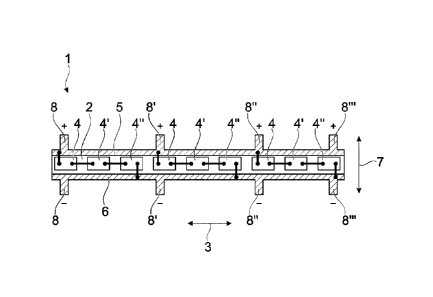
With reference now also to Fig. 2 of the drawings, a
schematic top view of an LED light emitting strip according
CA 03010745 2018-07-06
WO 2017/121773
PCT/EP2017/050515
to another embodiment is shown.
This embodiment differs from the embodiment of fig. 1 in
that a plurality of pairs of contact stripes 5', 6'; 5", 6"
are provided in a row along the length direction. Each pair
5 of contact stripes thereby corresponds to an individual
segment 9, 9', 9" of the LED light emitting strip.
Each segment 9, 9', 9" comprises a group of LED chips 4
contacted to the contact stripes 5, 6; 5', 6'; 5", 6" of the
corresponding pair. The respective pairs of contact stripes
10 are isolated or distanced from each other and configured to
supply the LED chips 4 of the respective group.
Each pair of contact stripes 5, 6; 5',6'; 5",6" is
configured individually controllable to individually actuate
or light the LED Chips of the corresponding segment 9, 9',
15 9" of the light emitting strip 1. This is realized in that
the terminals corresponding to each pair of contact stripes
are connected to an external control unit (not shown), which
is configured to individually provide a suitable supply
voltage and current for each terminal.
20 The LED light emitting strip and the control unit may be
comprised in an independent lighting. Alternatively or in
addition, a control unit may be implemented in a control
system of a vehicle. In this case, the lighting system
comprises the LED light emitting strip and is configured to
be connected to a control system of a vehicle.
Such a lighting system may comprise an arrangement of at
least two LED light emitting strips.
With reference now also to Fig. 3 of the drawings, a
schematic top view of an arrangement 100 of LED light
emitting strips 1, 1' is shown.
CA 03010745 2018-07-06
WO 2017/121773
PCT/EP2017/050515
21
As an example only, the first and second LED light emitting
strips 1, 1' are configured according to fig. 1. They are
shown in a section, which is near a connection region where
the first and second LED light emitting strips 1 and l' are
mated or joined. Furthermore, for a better overview only,
the contacts of the LED chips 4 are hidden in fig 3.
An end of the first light emitting strip 1 is mated or
joined with an end of the second light emitting strip 1'.
The connection between the mated or joined light emitting
strips 1, 1 can be realized in various ways. The connection
may be realized for example by means of a bracket, a
connector, or by means of firmly bonding the light emitting
strips, for example by soldering, welding or adhesive
bonding.
In particular, at least one of the contact stripes 5, 6 may
be configured to connect the light emitting strips, which
will be explained in more detail with respect to figs. 4 and
5.
A gap between the first and second LED light emitting strips
1, 1' may be free in the air (filled with air) or filled
with any light transmitting material, such as glass, a
transparent polymer, transparent epoxy resin or transparent
ceramic.
The LED chips 4 are arranged in a regular row with a
predetermined distance between them, which is a first
distance xl. The first and second light emitting strips are
mated or joined with each other in a butt configuration,
wherein a second distance x2 is provided between a last LED
chip 4' of the row of the first light emitting strip 1 and a
first LED chip 4" of the row of the second light emitting
strip 1'.
CA 03010745 2018-07-06
WO 2017/121773
PCT/EP2017/050515
22
The second distance is adapted to the first distance. Thus,
the LED light emitting strips 1, l' are connected to each
other with a connection invisible from outside, when the LED
light emitting strips are lighted.
In the exemplary embodiment shown, the first length xl is
equal to the second length x2. In other embodiments,
deviations are possible. A length of the second distance x2
thus is preferably at least 90 % of a length of the first
distance xl and the second distance x2 is equal to or less
than the sum x3 of the first distance xl and the length of
one LED chip 4. This results in a deviation or difference
between the first and second distances, which is hardly
recognizable from outside.
With reference now also to Fig. 4 of the drawings, a
schematic top view of an arrangement of LED light emitting
strips 1, 1' according to another embodiment is shown.
According to this embodiment, an end 10 of the contact
stripes 5, 6 is formed female or socket shaped. This is
realized, in that the end 10 of the contact stripes 5, 6
respectively extends over the corresponding end of the
substrate 2 of the light emitting strip 1. In this way, the
end 10 of the contact stripes 5, 6 is configured to
accommodate an end 12 of the substrate 2 of the second light
emitting strip 1' extending from an end 11 of the second
light emitting strip 1'.
The end 10 of the contact stripes 5, 6 is formed to enclose
the end 12 of the substrate 2 of the second light emitting
strip 1'. The light emitting strips 1, l' thus can be
connected to each other by inserting the end 12 of the
substrate 2 of the second light emitting strip 1 into the
female or socket shaped end 10.
CA 03010745 2018-07-06
WO 2017/121773
PCT/EP2017/050515
23
Finally, referring to Fig. 5 of the drawings, a schematic
top view of an arrangement of LED light emitting strips
according to yet another embodiment is shown.
According to this embodiment, an end 10 of the contact
stripes 5, 6 is also formed female or socket shaped.
However, in contrast to Fig. 4, this is realized, in that
the end 10 of the contact stripes 5, 6 respectively is
widened in the transverse direction 7. The end 10 of the
contact stripes 5, thus extends over the corresponding end
of the substrate 2 of the light emitting strip 1 in a
widened manner. In this way, the end 10 of the contact
stripes 5, 6 is configured to accommodate the complete end
11 of the second light emitting strip 1' including the ends
13 and 14 of the contact stripes 5, 6 thereof. The ends 13
and 14 thus can be directly connected mechanically and
electrically to the contact stripes 5, 6 of the first light
emitting strip 1.
The light emitting strips 1, 1' thus can be connected
mechanically and electrically to each other by inserting the
ends 13, 14 of the contact stripes 5, 6 of the second light
emitting strip 1' into the female or socket shaped end 10.
Although specific embodiments of the invention are
illustrated and described herein, it will be appreciated by
those of ordinary skill in the art that a variety of
alternate and/or equivalent implementations exist. It should
be appreciated that the exemplary embodiment or exemplary
embodiments are examples only and are not intended to limit
the scope, applicability, or configuration in any way.
Rather, the foregoing summary and detailed description will
provide those skilled in the art with a convenient road map
for implementing at least one exemplary embodiment, it being
CA 03010745 2018-07-06
WO 2017/121773
PCT/EP2017/050515
24
understood that various changes may be made in the function
and arrangement of elements described in an exemplary
embodiment without departing from the scope as set forth in
the appended claims and their legal equivalents. Generally,
this application is intended to cover any adaptations or
variations of the specific embodiments discussed herein.
It will also be appreciated that in this document the terms
"comprise", "comprising", "include", "including", "contain",
"containing", "have", "having", and any variations thereof,
are intended to be understood in an inclusive (i.e. non-
exclusive) sense, such that the process, method, device,
apparatus or system described herein is not limited to those
features or parts or elements or steps recited but may
include other elements, features, parts or steps not
expressly listed or inherent to such process, method,
article, or apparatus. Furthermore, the terms "a" and "an"
used herein are intended to be understood as meaning one or
more unless explicitly stated otherwise. Moreover, the terms
"first", "second", "third", etc. are used merely as labels,
and are not intended to impose numerical requirement on or
to establish a certain ranking of importance of their
objects.
PREFERRED EMBODIMENTS:
1. LED light emitting strip (1), in particular for an
automotive lighting system, comprising:
a substrate (2) extending along a length direction
(3) of the strip;
a plurality of LED chips (4) arranged on or in the
substrate (2), wherein the LED chips (4) are arranged
in at least one row along the length direction (3);
at least two contact stripes (5, 6) configured to
CA 03010745 2018-07-06
WO 2017/121773
PCT/EP2017/050515
supply the LED chips (4) with electric energy,
wherein each of the contact stripes (5, 6)
individually extends, at least partially, along a side
of the substrate (2) in the length direction (3), and
5 wherein the LED chips (4) are contacted to the
contact stripes (5, 6) at least partially in a
transverse or oblique direction (7) of the strip (1).
2. Light emitting strip according to embodiment 1, wherein
a surface of the substrate (2) is configured with a
10 high reflectance.
3. Light emitting strip according to embodiment 1 or 2,
wherein the substrate (2) is configured plastically
deformable.
4. Light emitting strip according to any of one of the
15 preceding embodiments, wherein the substrate (2)
comprises a metal.
5. Light emitting strip according to embodiment 4, wherein
the substrate (2) is formed integral with at least one
of the contact stripes (5; 6).
20 6. Light emitting strip according to anyone of the
preceding embodiments, wherein the at least two contact
stripes (5, 6) each comprise a plurality of, in
particular at least two, terminals (8) for additionally
applying supply voltage to the LED chips (4).
25 7. Light emitting strip according to embodiment 6, wherein
a first terminal (8') of a respective contact stripe
(5) is arranged at a section of the contact stripe (5)
distinct from the section of a second terminal (8").
8. Light emitting strip according to any one of the
CA 03010745 2018-07-06
WO 2017/121773
PCT/EP2017/050515
26
preceding embodiments, wherein at least one of the
contact stripes (5, 6) is configured for mating or
joining the light emitting strip (1) with another light
emitting strip (1').
9. Light emitting strip according to embodiment 8, wherein
an end (10) of at least one of the contact stripes (5,
6) is formed female or socket shaped and is configured
to accommodate an end (11) of the other light emitting
strip (1') or to accommodate an end (13; 14) of at
least one of the contact stripes (5, 6) of the other
light emitting strip (1') or to accommodate an end (12)
of the substrate (2) of the of the other light emitting
strip (1').
10. Light emitting strip according to anyone of the
preceding embodiments, wherein the LED chips (4) of at
least one part of the light emitting strip (1) are
contacted with the contact strips (5, 6; 5', 6'; 5",
6") in parallel to LED chips (4) of at least one other
part of the light emitting strip (1).
11. Light emitting strip according to anyone of the
preceding embodiments, wherein a plurality of pairs of
contact stripes (5, 6, 5', 6', 5", 6") are provided in
a row along the length direction (3) such that each
pair of contact stripes (5, 6, 5', 6', 5", 6")
corresponds to an individual segment (9, 9', 9") of the
light emitting strip.
12. Light emitting strip according to embodiment 11,
wherein the respective pairs of contact stripes (5, 6,
5', 6', 5", 6") are isolated or distanced from each
other and each pair of contact stripes (5, 6; 5', 6';
5",6") is configured to supply LED chips (4) of the
CA 03010745 2018-07-06
WO 2017/121773
PCT/EP2017/050515
27
corresponding segment (9; 9'; 9") of the light emitting
strip (1).
13. Light emitting strip according to embodiment 11 or 12,
wherein each pair of contact stripes (5, 6; 5', 6'; 5",
6") is configured individually controllable to
individually actuate or light the corresponding segment
(9; 9'; 9") of the light emitting strip (1).
14. Light emitting strip according to any one of the
preceding embodiments, wherein the LED chips (4)
arranged in the at least one row are positioned apart
from each other with a predetermined distance (x1).
15. An arrangement (100) of light emitting strips (1, 1'),
comprising:
a first light emitting strip (1) and a second
light emitting strip (1'), wherein at least one of the
first and second light emitting strips (1; 1') is
configured as light emitting strip according to one of
embodiments 1 to 14, and
wherein the first and second light emitting strips (1;
1') are mated or joined with each other.
16. The arrangement according to embodiment 15, wherein an
end (10) of the first light emitting strip (1) is mated
or joined with an end (11) of the second light emitting
strip (1').
17. An arrangement (100) of light emitting strips (1; 1'),
comprising:
a first light emitting strip (1) and a second
light emitting strip (1'), wherein at least one of the
first and second light emitting strips (1; 1') is
configured as light emitting strip according to
CA 03010745 2018-07-06
WO 2017/121773
PCT/EP2017/050515
28
embodiment 14,
wherein the predetermined distance (x1) between the LED
chips (4) arranged in the at least one row is a first
distance,
wherein the first and second light emitting strips (1;
1') are mated or joined with each other, and
wherein a second distance (x2) between a last LED chip
(4') of a row of the first light emitting strip (1) and
a first LED chip (4") of a row of the second light
emitting strip (1') is provided adapted to the first
distance.
18. The arrangement according to embodiment 17, wherein a
length of the second distance (x2) is at least 90 % of
a length of the first distance (x1).
19. The arrangement according to embodiment 17 or 18,
wherein the LED chips (4) have a uniform length, and
wherein the second distance (x2) is equal to or less
than the sum (x3) of the length of the first distance
(xl) and the length of one LED chip (4).
20. Method of manufacturing an arrangement of light
emitting strips, in particular an arrangement of light
emitting strips according to any one of embodiments 15
to 19, 10 comprising the steps of:
positioning a first light emitting strip (1)
relative to a second light emitting strip (1'), wherein
at least the first light emitting strip (1) comprises
at least two contact stripes (5, 6),
wherein each of the contact stripes (5, 6), at
least partially, extends along a side of a substrate
(2) of the first light emitting strip in a length
direction (3) of the first light emitting strip (1),
CA 03010745 2018-07-06
WO 2017/121773
PCT/EP2017/050515
29
wherein at least one of the contact stripes (5, 6) is
configured for mating or joining the first light
emitting strip (1) with the second light emitting strip
(1'); and
mating or joining the first and second light
emitting strips (1; 1') by means of the at least one of
the contact stripes (5, 6).
21. Method according to embodiment 20, wherein an end (10)
of the at least one of the contact stripes (5, 6) is
formed female or socket shaped and is configured to
accommodate an end (11) of the second light emitting
strip (1'), wherein the step of mating or joining the
first and second light emitting strips (1; 1') by means
of the least one of the contact stripes (5, 6)
comprises inserting the end (11) of the second light
emitting strip (1') into the female or socket shaped
end (10).
22. Method according to embodiment 21, wherein the female
or socket shaped end (10) is configured to accommodate
an end (13, 14) of at least one contact stripe of the
second light emitting strip (1'), wherein inserting the
end (11) of the second light emitting strip (1') into
the female or socket shaped end (10) comprises
inserting the end (13, 14) of the at least one contact
stripe of the second light emitting strip (1') into the
female or socket shaped end (10).
23. Method according to embodiment 21, wherein the female
or socket shaped end (10) is configured to accommodate
an end (12) of a substrate (2) of the second light
emitting strip (1'), inserting the end (11) of the
second light emitting strip (1') into the female or
CA 03010745 2018-07-06
WO 2017/121773
PCT/EP2017/050515
socket shaped end (10) comprises inserting the end (12)
of the substrate (2) of the second light emitting strip
(1') into the female or socket shaped end (10).
24. An automotive lighting system which comprises a light
5 emitting strip (1) according to any one of embodiments
1 to 14 or an arrangement (100) of light emitting
strips according to any one of embodiments 15 to 19 or
an arrangement of light emitting strips manufactured
according to a method of any one of embodiments 20 to
10 23.