Note: Descriptions are shown in the official language in which they were submitted.
CA 03010763 2018-07-06
WO 2017/153506
PCT/EP2017/055504
1
Analyte measuring patch
Field of disclosure
The present disclosure relates to the field of analyte measurement, in
particular glucose
measurement, in a body fluid or body tissue. It particular relates to the
design of
measurement and control circuitry for continuous analyte measurement.
Background, prior art
Continuous analyte measuring systems are known for the invasive and in-vitro
measurement of an analyte concentration in a patient's body fluid or tissue.
They are-
used, for example for the continuously monitoring a diabetic's glucose level
over an
extended time period of a number of days up to several weeks after which they
are
replaced, typically directly by the patient, a relative, or the like.
The sensors that are used in such system are typically based on an
amperometric
measurement principle and include a number of electrodes that are arranged on
a
typically elongated electrode carrier. For the application, an electrode-
carrying portion of
the electrode carrier is placed in the patient's subcutaneous tissue and the
glucose
concentration is measured in the interstitial fluid. A variety of sensor and
electrode
designs is known in the art. The sensor electrodes and the surrounding analyte-
comprising body fluid and/or tissue, in combination, form an electrochemical
cell. Where
not explicitly stated differently, such arrangement is also assumed in the
following.
CA 03010763 2018-07-06
WO 2017/153506
PCT/EP2017/055504
2
For operating such systems, sophisticated interface and measurement circuitry
is required
in addition to the sensor as such. In a typical design, the sensor includes
three electrodes,
namely a working electrode, a counter electrode and a reference electrode, and
the
interface and measurement circuitry is based on a circuit design generally
known as
potentiostat. In operation, the potentiostat applies a controlled and variable
voltage to
the counter electrode, thereby keeping the potential difference or voltage
between the
working electrode and the reference electrode at a given-constant level
(polarization
voltage). The current flowing between the counter electrode and the working
electrode is
correlated with the analyte concentrated and is measured for evaluation
purposes.
While a variety of potentiostat designs is known in the art and generally
available, a
number of constrains and boundary conditions is present in context of the here-
discussed
application, which have considerable impact on the potentiostat design and the
available
design options, resulting in many known designs being infeasible or at least
disadvantageous.
The interface and measurement circuitry is favourably arranged as close to the
sensor as
possible. It should accordingly be as small, compact and lightweight as
possible. The
electrode carrier is normally attached to an adhesive pad and projects from
the adhesive
pad that is placed on the patient's skin. For releasable electrical and
mechanical coupling
with the interface and measurement circuitry, a mechanical and electric
interface
zo structure is further provided typically directly on the patient's skin.
Classical potentiostat
designs, however, include a comparatively large number of complex components,
such
as several operational amplifiers (op-amps). It is further desirable to power
sensor and
circuitry with a single battery, e. g. a button cell. An asymmetric power
supply, however,
significantly increases the circuit complexity and number of required
electronic
components.
3
Since the involved voltages and currents at the sensor are small and directly
influence
the measurement results, contacting of the sensor is critical. While the
sensor with the
electrodes is a disposable that needs to be discarded after removal from the
tissue,
typical interface and measurement circuitry is too expensive to be discarded
after a
comparatively short application time. Costly and critical electrical
connectors are
accordingly required between sensor and circuitry.
It is an overall objective of the present invention to improve the state of
the art regarding
circuit designs of measurement circuitry for continuous analyte measurement,
in
particular continuous glucose measurement. Favourably, one or more of the
before-
io mentioned drawbacks of prior art solutions is avoided fully or partly.
The overall
objective is achieved by an analyte as described below.
Summary of disclosure
In an aspect, the overall objective is achieved by an analyte measuring patch
for invasive
is measuring a concentration of an analyte. The analyte measuring patch may
include a
sensor for transcutaneous placement in a patient's tissue, the sensor
including a working
electrode, a counter electrode and a reference electrode. The analyte
measuring patch
may further include a pad for placement on the patient's skin, wherein the
sensor
projects from an adhesive surface of the pad. The analyte may especially be
glucose, but
20 may also be an analyte that is present in a body fluid of a patient's
body. The body fluid
in which the analyte concentration shall be measured may, for example, be
blood or
Date recue/ date received 2022-02-18
CA 03010763 2018-07-06
WO 2017/153506
PCT/EP2017/055504
4
interstitial fluid, the latter being particularly favourably for the case of
glucose
concentration measurement.
The working electrode, the counter electrode and the reference electrode are
distinct
from each other and are separately operatively coupled to the electronics
unit, typically
via galvanic coupling. The electrodes are arranged on a rigid, semi-rigid or
soft electrode
carrier which projects from the adhesive surface of the pad substantially
perpendicular or
alternatively in a different angle for angular placement in the tissue.
Typically, the
electrode carrier is realized as elongated piece of substrate. In case of the
sensor being
semi-rigid or soft (not sufficiently stiff or rigid to allowing direct tissue
insertion), a rigid
auxiliary insertion element, e. g. in form of a cannula inside which the
sensor is placed for
the insertion, may be present. After successful insertion, the auxiliary
insertion element is
retracted out of the tissue. An insertion device may be present in order to
ensure a guided
an optionally automated, e. g. spring-driven, insertion process. Optionally,
such inserter
may be designed for e. g. automated retraction of the auxiliary insertion
element. The
design of suited sensors an insertion devices is generally known in the art.
The analyte measuring patch may further include an electronics unit, wherein
the
electronics unit includes a microcontroller and a current measurement unit.
The
microcontroller includes a control output, a first analogue input and a second
analogue
input. The control output is operatively coupled with a control electrode, the
control
zo electrode being either of the working electrode or the counter
electrode. The first
analogue input is operatively coupled with a measurement electrode via the
current
measurement unit, the measurement electrode being either of the working
electrode or
the counter electrode. The second analogue input is operatively coupled with
the
reference electrode. The microcontroller is configured to control, by
providing a control
CA 03010763 2018-07-06
WO 2017/153506
PCT/EP2017/055504
voltage to the control output, a potential difference between the working
electrode and
the counter electrode to equal a pre-defined polarization voltage.
The analyte concentration is determined by the electronics unit, typically by
the
microcontroller, by amperometric measurement of the current through the
measurement
5 .. electrode, using the current measurement unit.
In accordance with the present disclosure, the microcontroller serves,
together with
potential peripheral electronics, as digital potentiostat that controls a
potential of the
control electrode such that the potential difference between the working
electrode and
the reference electrode is kept substantially constant. For this purpose, the
microcontroller firmware is programmed to implement a digital closed loop
controller.
The pre-set polarization voltage as potential difference between the working
electrode
and the reference electrode defines the set point of the control loop. It may
be in a typical
range of, e. g. 100 Millivolt to 500 Millivolt, exemplarily 350 Millivolt. The
actual
potential difference between the working electrode and the reference electrode
defines
the actual value of the control loop. It is determined from the voltages
provided to the
first analogue input respectively second analogue input. For this purpose, the
microcontroller includes a first respectively second analogue-to-digital
converter (ADC)
that is associated with the first respectively second analogue input.
Alternatively, a single
ADC may be present that alternatively processes the voltages of the first
respectively
.. second analogue input, e. g. via multiplexing. The resolution of the ADCs
may, e. g. be 12
Bit. The difference between the actual potential difference (voltage between
working
electrode and reference electrode) and the pre-defined polarization voltage
defines the
control deviation of the control loop.
CA 03010763 2018-07-06
WO 2017/153506
PCT/EP2017/055504
6
Favourably, a reference voltage supply is present as part of the
microcontroller or as
separate part of the electronics unit, with the reference voltage being
maintained
constant for a varying supply voltage. Via this constant reference voltage and
the closed
loop controller, the polarization voltage between the reference electrode and
the working
electrode is maintained constant under varying conditions.
For the proposed design, a majority of structurally distinct and separate
electronics
components that is typically required for realizing a potentiostat can be
omitted and only
a small number of components is required in addition to the microcontroller.
The
microcontroller may be a commercially available state-of-the-art
microcontroller that
typically includes a number of analogue inputs as well as further input/output
interfaces.
For an arrangement in accordance with the present disclosure, the polarization
voltage
may be positive or negative in dependence of the sensor design. Furthermore,
current
flow may be from the working electrode to the counter electrode or vice versa.
Furthermore, either of the working electrode and the counter electrode may
serve as
control electrode and either of the working electrode and the counter
electrode may
serve as measurement electrode. A number of these variants will be discussed
in more
detail in the context of exemplary embodiments.
In some embodiments, the input voltage range that may be converted by the ADCs
at the
analogue inputs as well as the output voltage range at the analogue output
depend on
zo the supply voltage of the electronics unit. In an embodiment that is
assumed in the
following, the minimum voltage that may be converted equals or substantially
equals
zero (measured against ground), and the maximum voltage that may be converted
substantially corresponds to the (positive) supply voltage, i. e. the voltage
span
substantially equals the supply voltage.
CA 03010763 2018-07-06
WO 2017/153506
PCT/EP2017/055504
7
In some favourably embodiments that are also assumed in the following, the
microcontroller further includes an internal voltage reference, in particular
a voltage
reference for the analogue-to-digital conversion that provides a substantially
constant
absolute reference voltage over a large range of the battery supply voltage.
In this way,
the polarization voltage may be maintained at a constant absolute value even
though the
battery supply voltage varies. A voltage reference external to the
microcontroller,
however, may optionally be used.
In an embodiment, the electronics unit includes a voltage follower and the
reference
electrode is operatively coupled to the second analogue input via the voltage
follower.
The voltage follower may be realized based on an operation amplifier (op-amp)
as
generally known in the art. For accurate measurement results and in order to
avoid
potential sensor damage that may result from a current flow through the
reference
electrode, it is of major importance that the potential of reference electrode
is measured
in a static way, i. e. with the current flow through the reference electrode
being negligible.
Consequently, a current flow is present only between the working electrode and
the
counter electrode. In particular embodiments, the op-amp of the voltage
follower is the
only electronic component between the reference electrode and the second
analogue
input and the output of the voltage follower op-amp is directly galvanic
coupled to the
second analogue input and the reference electrode is favourably directly
galvanic coupled
to the non-inverting input of the voltage-follower op-amp. Within the context
of this
document, "direct galvanic coupling" means a coupling without electronic
components in
the flow path, but does not necessarily exclude the presence of electrical
contacts or
connectors.
In an embodiment, the microcontroller includes a digital-to-analogue converter
in
operatively coupling with the control output, and the control electrode is
operatively
CA 03010763 2018-07-06
WO 2017/153506
PCT/EP2017/055504
8
coupled to the control output via direct galvanic coupling or via a sample-and-
hold unit,
the sample-and-hold-unit preferably being a passive RC network. The control
output may
output the voltage continuously, in which case the control electrode is
favourably directly
galvanic coupled. For energy saving reasons, the control output may provide
the control
voltage only intermittently respectively periodically with a comparatively low
duty cycle.
In some embodiments, the duty cycle may be as lows as 5% to 10%. The absolute
frequency may be selected in a wide range from, e. g. 10 Hz up to several
hundred kHz.
A favourably passive "sample-and-hold" unit respectively low pass filter may
be provided
to continuously provide the control voltage to the control electrode with
sufficient
stability. Such "sample-and-hold" unit respectively low pass filter may be
realized by an
RC network as generally known in the art, e. g. with a single resistor and a
single
capacitor.
While one or more DACs are included in many state-of-the art microcontrollers,
this is not
necessarily the case. Alternatively to directly generating the control voltage
via a DAC, the
control output may be a digital binary output at which the microcontroller
outputs a
binary control signal with Pulse Width Modulation (PWM). In this case, a
passive low
pass filter RC network may be provided to generate the control voltage from
the pulse
width modulated signal.
In an embodiment, the current measurement unit includes a differential
amplifier unit or
a current-to-voltage converter unit.
Both differential amplifiers and voltage converters may be based on an op-amp
and
additional passive components, in particular resistors, as known in the art.
The circuitry
may further comprise additional components and/or functional units, in
particular
CA 03010763 2018-07-06
WO 2017/153506
PCT/EP2017/055504
9
inverting and/or non-inverting amplifiers, which are favourably also realised
based on
op-amps.
Exemplary and particularly favourably specific circuit designs are discussed
further below
in the context of exemplary embodiments.
In an embodiment, the control electrode is different from the measurement
electrode.
Alternatively, however, the control electrode and the working electrode may be
identical.
In an embodiment, the control electrode is the counter electrode and the
measurement
electrode is the working electrode. In an alternative embodiment with the
working
electrode being different from the measurement electrode, the control
electrode is the
working electrode and the measurement electrode is the counter electrode.
In an embodiment, the electronics unit is operatively coupled to or designed
for
operatively coupling to an asymmetric power supply, in particular a single-
voltage power
supply. An asymmetric power supply is favourable because it can be realized
with a single
battery of, e. g. the button cell type. An analyte measuring patch in
accordance with the
present invention can be favourably realized with an asymmetric power supply,
without
requiring a significant amount of additional circuitry or components.
In some embodiments, the potential of one of the working electrode or the
counter
electrode is fixed to a reference potential, e. g. ground, by direct galvanic
coupling.
In some embodiments, the potential of one of the electrodes, in particular the
counter
zo electrode, is shifted via corresponding circuitry for offset
compensation purposes and/or
to allow the measurement of a current between the working electrode and the
counter
electrode that is opposite to the standard current direction according to the
sensor and
CA 03010763 2018-07-06
WO 2017/153506
PCT/EP2017/055504
circuitry design. Such potential shifting may be realized via a potential
shifting unit which
may be realized via a passive RC network, a shifting voltage that is generated
via a DAC, a
PWM signal with associated filtering/smoothing circuitry, an additional
voltage reference
or voltage regulator, or the like.
5 .. In an embodiment, the microcontroller is configured to detect air bubbles
in contact with
at least one of the working electrode, the counter electrode and/or the
reference
electrode.
Air bubbles may be detected via corresponding algorithms that may be
implemented by
the microcontroller. The presence of air bubbles is reflected by considerable
signal
10 distortions. Air bubbles contacting or surrounding one or more of the
electrode result in
the analyte concentration measurement being inaccurate, and potentially the
analyte
concentration measurement being impossible.
Similarly, the microcontroller may be configured, via implementing
corresponding
algorithms, to detect further errors, defects, and/or hazardous situations,
such as
defective components or broken sensor connections. For this purpose, the
controller may,
e. g., be configured to temporarily vary the control voltage and/or
polarization voltage
according to a test schedule, e. g. once a day and for a short time period,
and detect
whether the signals as received from the sensor via the analogue inputs
reflect such
variation as expected.
zo In some embodiments, the microcontroller may further be configured to
execute further
routines associated with the analyte concentration measurement, such as a
separation of
AC and DC components of the measurement signal, and/or signal conditioning
like
smoothing, distortion/artefact removal, calibration, linearization, and the
like. Such
CA 03010763 2018-07-06
WO 2017/153506
PCT/EP2017/055504
11
routines or algorithms may include digital signal processing and filtering
algorithms as
generally known in the art, including adaptive filters, such as Kalman
filters.
Some or all of the before-described functionality, such as hazard/error
detection and
signal processing may alternatively or additionally be implemented on further
units or
devices of an analyte measurement system, as discussed further below in more
detail.
In an embodiment, the electronics unit and the sensor are non-detachably
mechanically
coupled. In such an embodiment, the sensor, the pad and the electronics
components of
the patch form a structurally compact and integral unit that is used for a
certain
application time and subsequently discarded as a whole. The circuitry is
favourably
arranged in a corresponding enclosure or housing and arranged on the non-
adhesive
surface of the pad, opposite to the sensor. Such enclosure or housing may
further include
a power supply, e. g. a button cell battery, and further components as
discussed further
below in the context of various system architectures. Favourably, the galvanic
coupling
between electrodes and circuitry is hard wired, thus avoiding releasable
electric
connectors.
In an embodiment, the sensor and the electronics unit are detachably
mechanically
coupled or designed to detachably mechanically couple. For this type of
embodiment,
releasable or detachable contacts are provided for the electric coupling of
sensor
electrodes and the electronics unit. Corresponding electrical and mechanical
interface
zo structures may be provided on the non-adhesive surface of the pad and an
enclosure or
housing of the electronics unit, thus providing a releasable or detachable
coupling e. g.
via snap-fit. For this type of embodiment, the pad and the sensor form a
common
disposable sensor and pad unit of comparatively short application time, while
the
application time of the electronics unit, favourably including the power
supply, may be
CA 03010763 2018-07-06
WO 2017/153506
PCT/EP2017/055504
12
significantly longer, e. g. in the range of a year or more and may be used
with a plurality
of sensor and pad units in sequence.
Some favourable examples for the overall system architecture of an analyte
measuring
patch are described in more detail further below in the context of exemplary
embodiments.
In an embodiment, the electronics unit includes a data communication unit, the
electronics unit being designed to exchange, via the data communication unit,
data, in
particular analyte concentration data or data correlated with analyte
concentration, with
a further electronics unit.
The data that are communicated may be processed analyte concentration data.
This is the
case in embodiments where the electronics unit, namely the microcontroller,
implements
the data processing algorithms and routines for computing an analyte
concentration,
such as routines and algorithms, for linearization calibration, filtering,
etc. Alternatively,
the data that are transmitted may be pre-processed measurement data or raw
data.
In an embodiment, the data communication unit is a wireless data communication
unit,
preferably a near field communication unit. Favourably, the electronics unit
is
environmentally sealed. The near filed communication unit may be an RFID
communication unit as commercially available or may another type of wireless
data
communication unit, such as an application specific inductive and/or
capacitive
zo communication unit. The environmentally sealing favourably provides a
sealing and
protection that allows the electronics unit to be used in typical everyday
situation,
including, e. g. showering or bathing.
CA 03010763 2018-07-06
WO 2017/153506
PCT/EP2017/055504
13
In an embodiment, the analyte measuring patch further includes a further
electronics unit,
the further electronics unit including a further data communication unit for
operatively
coupling with the data communication unit, the further electronics unit being
designed to
detachably mechanically couple to the electronics unit.
In such an embodiment, the electronics unit of the analyte measuring patch
mainly
includes the circuitry that is directly associated with the measurement. The
further
electronics unit may include one or more further microcontrollers,
microprocessors, data
storage, high-level signal evaluation and/or signal analysis unit, or the
like.
In an embodiment of the analyte measuring patch the electronics unit and the
further
electronics unit each include separate power supplies.
In an embodiment, the analyte measuring patch further includes a wireless
remote device
communication unit, the wireless remote device communication unit being
operatively
coupled to the microcontroller and being designed to exchange data, in
particular analyte
concentration data or data correlated with analyte concentration, with a
further separate
1 5 remote device.
In a further aspect, the overall objective is achieved by a method for
measuring a
concentration of an analyte, in particular glucose, and/or a method for
operating an
analyte measuring patch. The method includes providing an analyte measuring
patch.
The analyte measuring patch includes a sensor for transcutaneous placement in
a
zo .. patient's tissue. The sensor includes a working electrode, a counter
electrode and a
reference electrode, and a pad for placement on the patient's skin, wherein
the sensor
projects from an adhesive surface of the pad. The analyte measuring patch
further
CA 03010763 2018-07-06
WO 2017/153506
PCT/EP2017/055504
14
includes an electronics unit, wherein the electronics unit includes a
microcontroller and a
current measurement unit.
The method may include operatively coupling a control output of the
microcontroller with
a control electrode, the control electrode being either of the working
electrode or the
counter electrode. The method may further include operatively coupling a first
analogue
input of the microcontroller with a measurement electrode via the current
measurement
unit, the measurement electrode being either of the working electrode or the
counter
electrode. The method may further include operatively coupling a second
analogue input
of the microcontroller with the reference electrode. Alternatively, the
working electrode,
the counter electrode and the reference electrode may be operatively coupled
as part of
the analyte measuring patch prior to carrying out the method. The method may
further
include controlling, by providing a control voltage to the control output, a
potential
difference between the working electrode and the counter electrode to equal a
pre-
defined polarization voltage.
An analyte measuring patch in accordance with the present disclosure may be
used for
carrying out a method in accordance with the present disclosure. Therefore,
particular
embodiments of an analyte measuring patch disclose, at the same time,
corresponding
embodiments of a method for measuring the concentration of an analyte, and
vIce versa.
zo Brief description of figures
Fig. 1 shows an exemplary embodiment of an analyte measuring patch;
Fig. 2 shows a still further exemplary embodiment of an analyte measuring
patch;
Fig. 3 shows a still further an exemplary embodiment of an analyte
measuring patch;
CA 03010763 2018-07-06
WO 2017/153506
PCT/EP2017/055504
Fig. 4 shows an exemplary embodiment of a measurement and control circuit;
Fig. 5 shows a further exemplary embodiment of a measurement and control
circuit;
Fig. 6 shows a still further exemplary embodiment of a measurement and
control
circuit;
5 Fig. 7 shows a still further exemplary embodiment of a measurement
and control
circuit;
Fig. 8 shows a still further exemplary embodiment of a measurement and
control
circuit;
Fig. 9 shows a still further exemplary embodiment of a measurement and
control
10 circuit;
Fig. 10 shows a still further exemplary embodiment of a measurement and
control
circuit;
Fig. 11 shows a still further exemplary embodiment of a measurement and
control
circuit;
15 Fig. 12 shows a still further exemplary embodiment of a measurement and
control
circuit.
Exemplary embodiments
In the following, reference is first made to Fig. 1. Fig. 1 shows an exemplary
embodiment
zo analyte measuring patch 1 in accordance with the present disclosure in a
schematic
combined structural/functional view. Like in following further figures, the
specific
arrangement and relative locations of the individual elements do not imply any
particular
CA 03010763 2018-07-06
WO 2017/153506
PCT/EP2017/055504
16
design and/or geometric arrangement, unless explicitly stated differently. By
way of
example, the analyte is glucose and the analyte measuring patch 1 is designed
for
measuring glucose concentration inside the interstitial tissue.
The analyte measuring patch 1 includes a sensor 10, a pad 11, and an
electronics unit 12.
The sensor 10 includes an electrode carrier 100 that is designed for
transcutaneous
placement in a patient's tissue, either manually or using an insertion device.
In its
subcutaneous portion, i. e. its portion that is arranged under the skin during
application,
the electrode carrier 100 carries three electrodes, namely a working electrode
101, a
reference electrode 102, and a counter electrode 103, the three electrodes
being distinct
from each other. Suited sensor designs that may be used in the context of
analyte
measuring patch 1 are known in the art.
The pad 11 comprises an adhesive surface 110 that is designed to be attached
to the
patient's skin, with the sensor 10 respectively the electrode carrier 100
projecting from
the adhesive surface 110 perpendicularly (as exemplarily shown) or in another
desired
angle. The three electrodes 101, 102, 103 are in galvanic or wired connection
with a set
of corresponding set 104 of sensor contacts, that are arranged on a (typically
non-
adhesive) side of the pad 11 pointing away from the skin. A mechanical
interface
structure 111 is provided on the patch for releasable mechanical coupling with
an
electronics unit as described in the following and may include snap-fitting
elements,
zo catches,
latches, or the like as generally known in the art. In the shown embodiment,
the
sensor 10, the pad 11 and their associated components form a non-separable
disposable
unit that is designed to be used for a limited time of a number of days of up
to a number
of weeks and to be subsequently discarded.
CA 03010763 2018-07-06
WO 2017/153506
PCT/EP2017/055504
17
The electronics unit 12 includes a microcontroller-based digital potentiostat
unit 120, a
set 121 of electronics unit contacts, a supplementary electronics unit 122, a
remote
device communication unit 123, and a power supply in form of a single battery
124, e. g.
a button cell.
The before mentioned components of the electronics unit 12 are enclosed by a
housing
12. The housing 12 is designed for releasable engaging with the mechanical
interface
structure 111 on the pad. The contacts of the set 121 of electronics unit
contacts are
accessible from outside the housing and arranged such that they connect to the
corresponding contacts of the set 104 of sensor contacts upon engagement of
the
housing 125 and the mechanical interface structure 111, thus providing a
galvanic
coupling of the electrodes 101, 102, 103 and the digital potentiostat unit
120. In some
embodiments, the housing 125 is hermetically and environmentally sealed, in
particular
watertight, and is not designed to be opened. In such embodiments, the
battery124 may
be designed to provide power for the whole lifetime of, e.g. 6 or 12 months of
the
electronics unit 12, or may be rechargeable and be charged, e. g. via
inductive coupling
of additional charging contacts (not shown). Alternatively, the battery 124
may be
exchangeable. The electronics unit 12 is designed to be used in in combination
with a
plurality of disposable units in sequence.
The supplementary electronics unit 122 provides functionality that is required
in addition
zo .. to the digital potentiostat unit 120 and is operatively coupled with the
digital potentiostat
unit 120. It may provide functionality such as linearization, filtering,
calibration, data
storage, etc., as described above.
Via the remote device communication unit 123, the electronics unit 12 may
operatively
couple to and exchange data with a further remote device 2 e. g. according to
the
CA 03010763 2018-07-06
WO 2017/153506
PCT/EP2017/055504
18
Bluetooth standard or any other suited general purpose or proprietary
communication
standard and/or protocol. The further remote device 2 may, e. g. be a diabetes
management device of similar design and shape as a cell phone. The remote
device 2 is
typically used to show measured analyte values, analyte-versus-time graphs,
statistic
evaluations etc. The remote device 2 may further be designed for storing
measured
analyte concentrations, and may further be designed for coupling with still
further
devices, such as a Personal Computer (PC). The remote device may further be
used for
transmitting data, in particular calibration data, to the electronics unit.
In some embodiments, the electronics unit 1 and the remote device 2 are
designed to
.. operatively couple substantially continuously, with measured analyte
concentration data
being continuously transmitted to the remote device 2. Alternatively, the
electronics unit
may be designed to store the measured analyte concentration data internally,
e. g. in the
supplementary electronics unit, and transmit them from time to time according
to a fixed
schedule, or on demand, with the transmission being, e. g. initiated by a user
on the
remote device. In a further variant, only a single analyte concentration
value, e. g. blood
glucose value, is determined and transmitted to the remote device 2 on demand.
Alternatively to a diabetes management device the remote device 2 may be a
drug
delivery device, in particular an insulin pump. In such embodiment, analyte
concentration
data that are measured by the patch 1 are used for controlling drug
administration by the
zo drug delivery device, e. g. according to a closed loop or semi closed
loop as generally
known in the art. In a further embodiment, the electronics unit 12 is designed
to couple,
via its remote device communication unit 123, to a number of remote devices.
It is noted that the separation between the single functional units of the
electronics unit
12, in particular the separation between the digital potentiostat unit 120 and
the
CA 03010763 2018-07-06
WO 2017/153506
PCT/EP2017/055504
19
supplementary electronics unit 122, is for clarity reasons only and does not
imply a
particular technical implementation. Typically, the functionality of the
supplementary
electronics unit 122 is realized, fully or partly, by the same microcontroller
as used in the
digital potentiostat unit 120 and corresponding firmware. The supplementary
electronics
unit 122 and the digital potentiostat unit may accordingly also be considered
as common
unit.
In the following, reference is additionally made to Fig. 2. Fig. 2 shows a
further exemplary
embodiment analyte measuring patch 1 in accordance with the present disclosure
in a
schematic combined structural/functional view, similar to Fig. 1. Since the
embodiment
of Fig. 2 corresponds to the embodiment of Fig. 1 in a number of aspects, only
deviating
or differentiating features are discussed in the following.
In the embodiment of Fig. 2, the mechanical interface structure 111, the set
104 of
sensor contacts, 104, and set of electronics unit contacts, 121, are omitted.
Instead, the
electronics unit 12 respectively the electronic unit housing 125 is non-
detachably
attached to the pad 11, e. g. via gluing or ultrasonic welding. The housing 1
25
favourably encloses and capsules the components of the electronics unit 12 in
an
environmentally tight and in particular watertight way.
The embodiment of Fig. 2 has a number of advantages both from a technical and
a
handling or application point of view. As explained before, omitting lack of
releasable
zo electrical contacts between the electrodes 101, 102, 103 and the digital
potentiostat
circuit is technically favourable in view of the comparatively low potentials
respectively
voltages and currents involved. Furthermore, environmentally sealing is
easier. While the
embodiment of Figure 1 sealing means are favourably provided in the area of
the sets of
contacts, 104, 121, no such means are required in the embodiment of Fig. 2.
Due to the
CA 03010763 2018-07-06
WO 2017/153506
PCT/EP2017/055504
lack of releasable couplings and the accordingly reduced number of handling
steps,
everyday application is particularly simple. This aspect is of particular
relevance for
diabetic patients who are often visually and/or tactically impaired.
A drawback of the embodiment of Fig. 2 is the need to discard the whole
analyte
5 measuring patch 1 at the end of its comparatively short lifetime,
including in principle
reusable electronics components and battery. Long term application costs are
accordingly
critical. Thanks to the comparatively low number of costs of the required
electronic
components for the design of an electronics unit, namely a digital
potentiostat in
accordance with the present disclosure, it is feasible from an economic point
of view.
10 In the following, reference is additionally made to Fig. 3. Fig 3 shows
a further
embodiment of the analyte measuring patch 1. In this embodiment, the
electronics unit is
designed in a generally similar way as the embodiment of Fig. 2, with the
sensor 10, the
pad 11 and the electronics unit 12 favourably forming a common and on-
detachable unit
and in particular a unit direct galvanic coupling between electrodes 101, 102,
103 and
15 digital potentiostat circuit 120.
In contrast to the embodiment of Fig. 2, however, the electronics unit 12
comprises a
data communication unit 126, in particular a Near Field Communication (NFC)
unit such
as an RFID unit.
A further electronics unit 13 with a further electronics unit housing 135 is
present. The
20 electronics unit 12 and the further electronics unit 1 3 are designed
for reliably coupling
via a coupling structure 137. Favourably, the further electronics unit housing
135
environmentally seals the further electronics unit 13.
CA 03010763 2018-07-06
WO 2017/153506
PCT/EP2017/055504
21
The further electronics unit 13 includes a further data communication unit 136
that is
designed to exchange and in particular receive data from the data
communication unit
126. The further electronics unit 1] further includes an electronics module
130 in
operative coupling with the further data communication unit 136 and
essentially takes
over the functionality of the supplementary electronics unit 122 in the
alternative
embodiments of Fig1 and Fig. 2. The electronics module 130 is operatively
coupled with
a wireless remote device communication unit 133 for data exchange with a
remote
device 2 as discussed above. The further electronics unit 13 is powered via
further
electronics unit power supply 134, e. g. a battery. In contrast to the
electronics unit 12,
the further electronics unit 13 is reusable and designed to be uses for an
extended
lifetime.
The embodiment of Fig. 3 shows the same advantage as the embodiment of Fig. 2
that
no releasable contacts are required for connecting the sensor 10 and that the
electronics
unit housing 125 can be favourably designed to be environmentally sealed. In
addition,
the battery 124 may be smaller since as compared to the embodiment of Fig. 2
since it
powers less components and only near-filed data communication is required. In
addition,
fewer electronics components are present in the disposable electronics unit
12. In
particular, comparatively expensive components, such as the remote device
communication unit 133 (e. g. a Bluetooth module as explained before) are non-
disposable.
In a variant, the supplementary electronics unit 122 is still present in the
electronics unit
and carries out tasks such as filtering, calibration and/or linearization,
while the
electronics module 130 is used for high-level data evaluation, data storage
etc. In a
further variant, the electronics unit.
CA 03010763 2018-07-06
WO 2017/153506
PCT/EP2017/055504
22
In a further variant, the power supply or battery 124 of the electronics unit
12 is omitted
and the electronics unit 12 is supplied from the further electronics unit e.
g. via inductive
coupling.
Independent of the specific type of embodiment, alarming device, e. g. an
acoustic
alarming device in form of an acoustic transducer and/or an tactile alarming
device in
form of a pager vibrator, may optionally be present in order to provide an
alarm to the
user e. g. in case of a device fault or a critical situation regarding the
measured analyte
concentration, e. g. a situation of hypoglycemia or hyperglycemia in case of
the analyte
being glucose. For the embodiment of Fig. 1, or Fig. 2, an alarming device may
be part of
the disposable electronics unit, e. g. the supplementary electronics unit 122.
In the
embodiment of Fig. 13, an alarming device may favorably be part of the further
electronics unit 13, e. g. part of the electronics module 130.
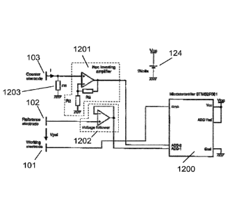
In the following, reference is additionally made to Fig. 4. Fig. 4 shows a
circuit diagram of
an exemplary measurement and control circuit or digital potentiostat circuit
120 in
accordance with the present disclosure. The digital potentiostat circuit 120
includes a
microcontroller 1200, a non-inverting amplifier 1201, a voltage follower 1202,
and a
current-to-voltage converter 1203. As explained before, the microcontroller
may
additionally be configured or programmed to carry out further tasks. It is
noted that the
indicated type of microcontroller is exemplary and may be replaced by a
variety of other
zo microcontrollers.
In Fig. 4 and further exemplary embodiments, as well as in the description,
the following
convention is used. The polarization voltage Vpol is considered to be positive
if the
potential of the reference electrode is lower than the potential of the
working electrode.
The current between the working electrode and the counter electrode is
considered
CA 03010763 2018-07-06
WO 2017/153506
PCT/EP2017/055504
23
positive if it flows from the working electrode into the counter electrode, as
indicated by
the corresponding voltage and current arrows in the circuit diagrams. Other
conventions,
however, may be used as well.
In the embodiment, the current between working electrode and counter electrode
is
converted into a proportional voltage by current-to-voltage converter 1203 in
form of
resistor R1 that is connected to the counter electrode 103. This voltage is
fed into an op-
amp based non-inverting amplifier 1201 and fed into a first analogue input ADC-
2 of the
microcontroller 1200. The counter electrode accordingly serves as measurement
electrode.
The reference electrode 102 is coupled to a second analogue input ADC-1 of the
microcontroller 1200 via a voltage follower 1202. The voltage follower 1202
serves as
impedance converter of virtually infinite input impedance and ensures that the
voltage at
the second analogue input corresponds to the voltage of the reference
electrode 102
(measured against ground), but there is no current flow through the reference
electrode
102. The only current flow is between the working electrode 101 and the
counter
electrode 103.
The working electrode 101 is directly galvanic coupled to a control output DAC
of a
digital-to-analogue converter of the microcontroller 1200. The working
electrode
accordingly serves as control electrode.
The microcontroller 1200 is programmed to output a control voltage at the
control
output ¨ thereby adjusting the current between working electrode 101 and the
counter
electrode 103 ¨ such that the voltage between the working electrode 101 and
the
reference electrode 102 corresponds to the preset polarization voltage.
Updating and
CA 03010763 2018-07-06
WO 2017/153506
PCT/EP2017/055504
24
outputting the control voltage is carried out repeatedly or virtually
continuously, e. g. 1 to
50 times per second.
In the circuit diagram of Fig. 4, like in further circuit diagrams as
described further below,
a voltage supply that is connected to connector Vref of the microcontroller
1200 provides
a supply voltage for an internal voltage reference of, e. g. 1.2 V of the
microcontroller
1200. The voltage of the voltage reference however, is not dependent on the
precise
voltage supplied to Vref which accordingly does not need to be stabilized. It
may
therefore be simply connected to the battery 124 and is supplied with the
battery voltage
Vcc. The minimum and maximum voltage that may be converted by the ADCs and DAC
of the microcontroller 12000 is, as described before, defined by Vcc.
In the following, reference is additionally made to Fig. 5. Fig. 5 shows a
further
embodiment of the digital potentiostat circuit 120. In principle, the design
as shown in
Fig. 5 is similar to the design as shown in Fig. 4. However, in the design of
Fig. 5, the
working electrode 101 serves as both measurement electrode and control
electrode,
while the counter electrode 103 is galvanic coupled to ground, which is
advantageous
with respect to stability. In this embodiment, the working electrode 101 is
connected to
both the negative/inverting input of an op-amp based differential amplifier
1203 and a
third analogue input ADC-3 of a third analogue-to-digital converter. The
positive/non-
inverting input of the differential amplifier 1204 is coupled to the control
output DAC,
and the output of the differential amplifier 1204 is coupled to the first
analogue input
ADC-2. R1 is a resistor defining the input impedance (impedance between
positive/non-
inverting and negative/inverting input) and resistor Rgain defines the gain of
differential
amplifier 1204. In this embodiment, a third analogue input and a third
analogue-to-
digital converter are required in order to compensate the voltage drop over
the input
impedance R1.
CA 03010763 2018-07-06
WO 2017/153506
PCT/EP2017/055504
In the following, reference is additionally made to Fig. 6. Fig. 6 shows a
further
embodiment of the digital potentiostat circuit 120. In the embodiment, the
counter
electrode 103 serves as control electrode and is directly coupled to the
control output
DAC. The working electrode 101 serves as measurement electrode and is
connected to
5 the first analogue input ADC-2 via a series of an (inverting) current-to-
voltage converter
1203 and an inverting op-amp based amplifier 1205. In this example, the
current-to-
voltage converter 1203 is also op-amp based.
In the embodiment of Fig. 6, a further external 2.5V reference voltage supply
124a is
provided that is connected to the non-inverting inputs of the op-amps of the
current-to-
10 voltage converter 1203 and an inverting op-amp based amplifier 1205. In
this example,
the current- to voltage converter 1203 has an output voltage of 2. 5V
(reference voltage
as supplied by external reference voltage supply 124) and Vcc, while the
inverting
amplifier 1205 provides an output voltage 0 ... 2.5V. Further in the example,
the
connector Vref of the microcontroller 1200 is coupled to the external
reference voltage
15 .. supply 124a, which, however, is not essential.
In the following, reference is additionally made to Fig. 7. Fig. 7 shows a
further
embodiment of the digital potentiostat circuit 120. Like in the embodiment of
Fig. 4, the
working electrode 101 serves as control electrode, while the counter electrode
103
serves as measurement electrode. In contrast to the embodiment of Fig. 4,
however, the
zo .. counter electrode 103 / measurement electrode is coupled to the first
analogue input
ADC-2 via differential amplifier 1204.
In the following, reference is additionally made to Fig. 8. Fig. 8 shows a
further
embodiment of the digital potentiostat circuit 120. In most aspects, the
embodiment of
Fig. 8 is similar to the embodiment of Fig. 7.However, an additional RC-
network 1206 is
H8324993CA
26
present in this embodiment which serves as potential shifting unit and shifts
the potential
of the counter electrode 103. Shifting the counter electrode potential may be
favorable to
allow the detection of negative current and/or compensate the offset of the op-
amp in non-
inverting amplifier1201, A third analogue input ADC-3 of the microcontroller
1200 is used in
this embodiment to measure the potential shift.
In the following, reference is additionally made to Fig. 9. Fig. 9 shows a
further embodiment
of the digital potentiostat circuit 120. In most aspects, the embodiment of
Fig. 9 is similar to
the embodiment of Fig. 8. However, the counter electrode 103 is coupled to the
first
analogue input ADC-2 via a differential amplifier 1204 rather than non-
inverting amplifier
3.0 1201. The counter electrode 103 is coupled to the positive/non-
inverting input and the shift
voltage as determined by RC-network 1206 is fed into the negative-inverting
input of
differential amplifier 1204. In contrast to the embodiment of Fig. 8, the
embodiment of Fig.
9 does not require the third analogue input.
In the following, reference is additionally made to Fig. 3Ø Fig. io shows a
further
embodiment of the digital potentiostat circuit 120. The embodiment of Fig. 10
is
designed for a positive polarization voltage and negative current
between working
electrode 101 and counter electrode 103 and requires a particularly small
number of
components for this configuration. In the embodiment of Fig. io, the counter
electrode
103 is coupled to the control output DAC and accordingly serves as control
electrode.
The working electrode ioi serves as measurement electrode and is coupled to
the first
analogue input ADC-2 via op-amp based current-to-voltage converter 1203, with
the
positive/non-inverting input of the op-amp being coupled to the supply
voltage.
Alternatively to voltage-to current converter 1203, a differential amplifier
could be used
for the current measurement. In further variants, the working electrode ioi
serves as
control electrode and current measurement is performed at the counter
electrode 103
Date Recue/Date Received 2021-09-08
CA 03010763 2018-07-06
WO 2017/153506
PCT/EP2017/055504
27
and either of the working electrode 101 or the counter electrode 103 serve
serves as
measurement electrode.
In the following, reference is additionally made to Fig. 11. Fig. 11 shows a
further
embodiment of the digital potentiostat circuit 120. The embodiment of Fig. 11
is
designed for a negative polarization voltage and positive current between
working
electrode 101 and counter electrode 103 and requires a particularly small
number of
components for this configuration. The embodiment of figure 11 is similar to
the
embodiment of Fig. 10. As sole difference, the positive/non-inverting input of
the op-
amp is coupled to ground rather than to the supply voltage.
In a variant, the working electrode 101 serves as control electrode and the
current is
measured via a voltage-to-current converter at the counter electrode which
accordingly
serves as measurement electrode.
In the following, reference is additionally made to Fig. 12. Fig. 12 shows a
further
embodiment of the digital potentiostat circuit 1 20. The embodiment of Fig. 12
is
designed for a negative polarization voltage and a negative current between
working
electrode 101 and counter electrode 103 and requires a particularly small
number of
components for this configuration. The embodiment of Fig. 12 is similar to the
embodiment of Fig. 4. As sole difference, the role of control electrode and
measurement
electrode is reversed. In the embodiment of Fig. 4, the counter electrode 103
serves as
zo measurement electrode and is coupled to the first analogue input ADC-2
via the non-
inverting amplifier 1201. In the embodiment of Fig. 12, in contrast, the
working
electrode 1 01 serves as measurement electrode and is coupled to the first
analogue input
ADC-2 via the non-inverting amplifier 1201. Similarly, in the embodiment of
Fig. 4, the
working electrode 101 serves as control electrode and is directly coupled to
the control
CA 03010763 2018-07-06
WO 2017/153506
PCT/EP2017/055504
28
output DAC. In the embodiment of Fig. 12, in contrast, the counter electrode
103 serves
as control electrode and is directly coupled to the control output DAC.
In a variant, current is measured using a differential amplifier on either of
the working
electrode 101 or the counter electrode 103. In a further variant, the working
electrode
101 serves as control electrode and the current is measured at the working
electrode 101
or the counter electrode 103 using a differential amplifier.
As mentioned before, a ¨ favorably passive ¨ sample-and-hold unit may
generally be
used in the before-described embodiments in the coupling of control output and
control
electrode in order to reduce the energy consumption.