Note: Descriptions are shown in the official language in which they were submitted.
CA 03011489 2018-07-13
WO 2017/186150 PCT/CN2017/082278
LED LIGHT BULB
RELATED APPLICATIONS
[0001] The present application claims priority to CN201610281600.9 filed
April 29,
2016, CN201610272153.0 filed April 27, 2016, CN201610394610.3 filed June 3,
2016,
CN201610586388.7 filed July 22, 2016, CN201610544049.2 filed July 7, 2016,
CN201610936171.4 filed November 1, 2016 and CN201611108722.4 filed December 6,
2016,
CN201710024877.8 filed January 13, 2017, CN201710079423.0 filed February 14,
2017,
CN201710138009.2 filed March 9, 2017, CN201710180574.5 filed March 23, 2017,
CN
201710234618.8 filed April 11, 2017, each of which is incorporated herein by
reference in its
entirety.
[0002] If (1) a term in the present application conflicts with the term
used in a
previous application to which the present application claims priority, or (2)
conflicts with a
term in an application incorporated by reference (2a) into the present
application or into (2b) an
application to which the present application claims priority, a construction
based on the term as
used or defined in the present application prevails
FIELD OF THE INVENTION
[0003] The present invention relates to LED luminaries. More
particularly, this
invention describes an LED light bulb having an LED filament.
BACKGROUND OF THE INVENTION
[0004] Incandescent light bulbs are a source of electric light that
creates light by
running electricity through a resistive filament, thereby heating the filament
to a very high
temperature, so that it glows and produces visible light. Incandescent bulbs
are made in a wide
range of sizes and voltages, from 1.5 volts to about 300 volts. The bulbs
consist of a generally
glass or plastic enclosure with a filament of tungsten wire inside the bulb
through which an
electrical current is passed. Incandescent lamps are designed as direct "plug-
in" components
that mate with a lampholder via a threaded Edison base connector (sometimes
referred to as an
"Edison base" in the context of an incandescent light bulb), a bayonet-type
base connector (i.e.,
1
CA 03011489 2018-07-13
WO 2017/186150 PCT/CN2017/082278
bayonet base in the case of an incandescent light bulb), or other standard
base connector to
receive standard electrical power (e.g., 120 volts A.C., 60 Hz in the United
States, or 230V
A.C., 50 Hz in Europe, or 12 or 24 or other D.C. voltage). The base provides
electrical
connections to the filament. Usually a stem or glass mount anchors to the
base, allowing the
electrical contacts to run through the envelope without gas or air leaks.
[0005] Incandescent light bulbs are widely used in household and
commercial
lighting, for portable lighting, such as table lamps, car headlamps,
flashlights, and for
decorative and advertising lighting. However, incandescent light bulbs are
generally
inefficient in terms of energy use and are subject to frequent replacement due
to their limited
lifetime (about 1,000 hours). Approximately 90% of the energy input is emitted
as heat. These
lamps are gradually being replaced by other, more efficient types of electric
light such as
fluorescent lamps, high-intensity discharge lamps, light emitting diodes
(LEDs), etc. For the
same energy input, these technologies give more visible light and generate
much less heat.
Particularly, LEDs consume a fraction of the energy used to illuminate
incandescent bulbs and
have a much longer lifetime (e.g. 50,000 to 75,000 hours). Furthermore, LED
light sources are
a very clean "green" light source and also provide good color reproduction.
[0006] LED light bulbs are far more efficient than traditional
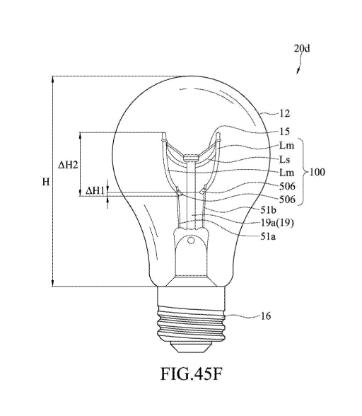
incandescent lamps,
most notably because they use only a small fraction of the electricity of an
incandescent. As
traditional incandescent bulbs continue to be phased out, LED has become the
mainstream
light sources used on a variety of indoor and outdoor lighting fixtures.
However, traditional
LED light bulbs are not without its disadvantages, for example, the
complicated designs which
incorporate the heavy aluminum heat sinks and an electronic circuit for power
conversion.
Consequently, the cost is high and the shape is somewhat strange compared with
the elegant
incandescent bulbs people are accustomed to.
[0007] An LED filament bulb is a light bulb that uses LEDs as its
filaments.
Accordingly, it is desirable to provide a novel LED filament light bulb with
improved
performance and aesthetics that may be used as a better replacement for a
typical incandescent
light bulb than traditional LED light bulbs.
[0008] The LED has advantages of environmental protection, energy
saving, high
efficiency and long lifespan, and therefore it attracts widespread attention
in recent years and
gradually replaces traditional lighting lamps. However, due that the
luminescence of the LED
2
CA 03011489 2018-07-13
WO 2017/186150 PCT/CN2017/082278
has directivity, current LED lamps is unable to provide with an illumination
with a wide angle
range like traditional lamps. Accordingly, how to design LED lamps with
similar wide range
of illumination to the traditional lamps challenges the industries.
[0009] Recently, an LED light bulb has been provided and gradually
replaces the use
of incandescent light bulbs. The kind of the LED light bulbs is provided with
multiple LED
filaments due to the limited illuminating angle of LED light sources. The LED
filaments are
aligned in a circle in the LED light bulb, and each of the LED filaments faces
different angles
for illumination, such that the illuminating angle of the LED light bulb could
be increased in
general. The manufacturing process of the LED filament includes: fixing
multiple LED chips
in series to a long, narrow glass substrate, enclosing the whole glass
substrate by silicone gel
mixed with phosphor powders, and processing electrical connection of the LED
filament.
When the LED filaments are welded to a stand in the LED light bulb, the LED
filaments have
to be welded one by one, which is numerous and complicated. Further, the LED
filaments are
welded in a spot welding manner, which requires high standard regarding
property and size of
materials, and has a risk of faulty welded joint. In appearance, the LED
filaments are hard and
straight and lack flexibility and variation. The conventional LED light bulb
gives people
nothing more than a visually stiff feeling and cannot provide an aesthetic
appearance.
[0010] In addition, the color temperature of light generated by the LED
filaments is
usually too high such that the use of the LED filaments is only suitable for
limited
environments. In a comfort and relax occasion, using conventional tungsten
filament bulbs
with low color temperature of light for illumination is much better.
[0011] Further, the LED filaments generate a large amount of heat during
operation.
Heat may damage components in the LED light bulb such as LED chips and a
driving circuit
and lower the efficiency of the LED filaments.
OBJECTS AND SUMMARY OF THE INVENTION
[0012] It is an object of the present invention that light is emitted
from one or more
LED filaments uniformly and evenly in all directions, instead of beaming in a
direction while
leaving everywhere else dark the way that many traditional LED light bulbs do.
Thus, the LED
filament light bulb features a close resemblance with the traditional
incandescent bulb.
Desirably, the visually unpleasant aluminum die cast for heat dissipation in
traditional LED
3
CA 03011489 2018-07-13
WO 2017/186150 PCT/CN2017/082278
light bulbs is no longer required in the LED filament light bulb. Thus, the
LED filament light
bulb is perfect for homes, hotels, restaurants, bars and places where classic
style and
appearance is critical. Desirably, all electronics of the LED filament light
bulb is nestled inside
the light bulb which is almost not visible. Desirably, light produced by the
LED filament light
bulb is similar to natural light. It does not have any infrared or ultraviolet
radiation and it is
uniform and soft on the eyes. After the regulations that banned the sale of
the traditional light
bulbs, many homeowners could not put in compact fluorescent bulbs or other
bogus LED
lights into most of these old fixtures and chandeliers. Desirably, the LED
filament light bulb
fits well into all the lighting fixtures that used the outdated incandescent
light bulbs. Desirably,
the LED filament light bulb makes it easy to reuse these old and attractive
lighting fixtures.
Desirably, the LED filament light bulb have remarkable energy efficiency.
Desirably, the LED
filament has a long service life. This extended lifespan is enhanced by a
constant current
source that ensures stability of parameters and prolongs the life of the light
bulb. Hence, the
cost of investing in these bulbs will provide cost savings for up to a few
decades in some cases.
Desirably, the LED filament light bulb can be placed in places where dimming
of lights is
necessary. The LED filament light bulb gives off a warm inviting golden soft
glow when used
in table lamps or as accent lights. The LED filament light bulb is perfect for
creating a very
pleasant atmosphere in sitting rooms or bedrooms.
[0013] Therefore, it is an object of the claimed invention to provide a
significantly
improved LED filament for using with an LED light bulb. In accordance with an
embodiment
with the present invention, the LED filament configured for emitting
omnidirectional light,
comprising: a linear array of LED chips operably interconnected to emit light
upon
energization; a conductive electrode; the linear array of LED chips is
electrically connected
with the conductive electrode; and a light conversion coating enclosing the
linear array of the
LED chip and the conductive electrode, wherein: the light conversion layer
includes a top layer
and a base layer conformally interconnected to form a unitary enclosure; the
top layer is coated
on a first side of the linear array of LED chips and the conductive electrode;
and the base layer
is coated on a second side of the linear array of LED chips and the conductive
electrode.
[0014] It is an object of the claimed invention to provide an improved
LED light
bulb, which is easily manufactured, has a wide angle for illumination, and
provides an
aesthetic appearance.
4
CA 03011489 2018-07-13
WO 2017/186150 PCT/CN2017/082278
[0015] In accordance with an embodiment with the present invention, an
LED light
bulb, comprises: a bulb shell; a stem disposed inside the bulb shell; at least
two conductive
supports connected to the stem; an LED filament comprising two conductive
electrodes; and at
least one supporting arm with an end connected to the stem and an another end
connected to
the LED filament; wherein points of the LED filament in an xyz coordinates is
defined as X, Y,
and Z and satisfies a curve equation, an origin of the xyz coordinates is at
the stem top, an x-y
plane of the xyz coordinates passes through the stem top and is perpendicular
to the height
direction, a z-axis of the xyz coordinates is coaxial with the stem, and the
two conductive
electrodes are disposed at two sides of a y-axis of the xyz coordinates, the
curve equation is:
X=ml*cos(t*360), Y=m2*sin(t*360), Z=n*cos(t*360*k), wherein, t is a variable
between 0
and 1, the LED filament varies along an x-direction, a y-direction, and a z-
direction according
to t; wherein, when X=0, a max value of IYI is m2, and a max value of IZI is
n; wherein, when
Y=0, a max value of IXI is ml, the max value of IZI is n; wherein, when Z=0,
the max value of
IXI is ml, and the max value of IYI is m2; wherein, ml is a length in the x-
direction, m2 is a
length in the y-direction, n is a height of the highest point from the x-y
plane in the z-direction,
and k is a number of the highest point(s).
[0016] In accordance with an embodiment with the present invention, the
LED light
bulb emits omnidirectional light.
[0017] In accordance with an embodiment with the present invention, the
value k is
greater than or equal to 2 and is less than or equal to 8.
[0018] In accordance with an embodiment with the present invention,
cross sections
of the bulb shell on the horizontal plane from the bottom to the top of the
bulb shell along the
height direction have varied radii, r is the largest value of the varied
radii, wherein ml is set as:
O. 8*r<m 1 <0.9*r.
[0019] In accordance with an embodiment with the present invention,
cross sections
of the bulb shell on the horizontal plane from the bottom to the top of the
bulb shell along the
height direction have varied radii, r is the largest value of the varied
radii, wherein m2 is set as:
O. 8* r<m2<0. 9*r.
[0020] In accordance with an embodiment with the present invention,
cross sections
of the bulb shell on the horizontal plane from the bottom to the top of the
bulb shell along the
CA 03011489 2018-07-13
WO 2017/186150 PCT/CN2017/082278
height direction have varied radii, r is the largest value of the varied
radii, wherein n is set as :
< n<0.47*r.
[0021] In accordance with an embodiment with the present invention, the
value ml is
greater than or equal to 24 mm and is less than or equal to 27 mm.
[0022] In accordance with an embodiment with the present invention, the
value m2 is
greater than or equal to 24 mm and is less than or equal to 27 mm.
[0023] In accordance with an embodiment with the present invention, the
value n is
greater than 0 and is less than or equal to 14 mm.
[0024] In accordance with an embodiment with the present invention, a
projection of
the LED filament on the x-y plane is a quasi-circle, 0 is an angle of an arc
formed by the
projection, the arc angle 0 is from 180 to 360 , wherein a relation between
the LED filament
varying along the z-axis and 0 satisfies a function, the function is:
Z=n*cos(k0+
[0025] According to the embodiments of the instant disclosure, the LED
light bulb
includes many advantages. For example, the manufacturing of the product is
simplified, the
angle of emitting light is wide, the color temperature of light could be
easily adjusted, the
strength of the filament is better, and the whole of the product has a better
aesthetic appearance.
The LED light lamp is capable to emit omnidirectional light. Moreover, The LED
light lamp
may also need the least length and the least number of the LED chips while
emitting
omnidirectional light. As a result, the cost of materials for the manufacture
of the LED light
bulb may reduce, and the temperature of the LED light bulb during operation
can be
suppressed.
[0026] Various other objects, advantages and features of the present
invention will
become readily apparent from the ensuing detailed description, and the novel
features will be
particularly pointed out in the appended claims.
BRIEF DESCRIPTION OF FIGURES
[0027] The following detailed descriptions, given by way of example, and
not
intended to limit the present invention solely thereto, will be best be
understood in conjunction
with the accompanying figures:
[0028] FIG. 1 is a see-through view of the LED filament in accordance
with an
embodiment of the present invention;
6
CA 03011489 2018-07-13
WO 2017/186150 PCT/CN2017/082278
[0029] FIG. 2 is a see-through view of the LED filament in accordance
with an
embodiment of the present invention;
[0030] FIG. 3 is a see-through view of the LED filament in accordance
with an
embodiment of the present invention;
[0031] FIG. 4 includes a see-through view and a cut-open view of the LED
filament
in accordance with an embodiment of the present invention;
[0032] FIGs. 5A to 5D are schematic views of the electrical connector in
accordance
with an embodiment of the present invention;
[0033] FIGs. 5E and 5F are top views of conductive electrodes of
filaments in
accordance with an embodiment of the present invention;
[0034] FIG. 5G is a side view of conductive electrodes of a filament in
accordance
with an embodiment of the present invention;
[0035] FIGs. 5H, 51 and 5J are top views of conductive electrodes of
filaments in
accordance with an embodiment of the present invention;
[0036] FIGs. 6A to 6H are schematic views of the LED device in
accordance with an
embodiment of the present invention;
[0037] FIGs. 7A to 7D are schematic views of the linear array of LED
devices in
accordance with an embodiment of the present invention;
[0038] FIGs. 8A to 8F are schematic views of the linear array of LED
devices in
accordance with an embodiment of the present invention;
[0039] FIGs. 9A and 9B are schematic views of the LED filament in
accordance with
an embodiment of the present invention;
[0040] FIGs. 10A to 10C are schematic views of the LED filament in
accordance
with an embodiment of the present invention;
[0041] FIGs. 11A to 11C are schematic views of the LED filament in
accordance
with an embodiment of the present invention;
[0042] FIGs. 12A to 12D are schematic views of the LED filament in
accordance
with an embodiment of the present invention;
[0043] FIG. 13 is a front view of the LED light bulb in accordance with
an
embodiment of the present invention;
7
CA 03011489 2018-07-13
WO 2017/186150 PCT/CN2017/082278
[0044] FIG. 14 is a cutaway view of the LED filament in accordance with
an
embodiment of the present invention;
[0045] FIG. 15 is a cutaway view of the LED filament in accordance with
an
embodiment of the present invention;
[0046] FIG. 16 is a cutaway view of the LED filament in accordance with
an
embodiment of the present invention;
[0047] FIG. 17 is a cutaway view of the LED filament in accordance with
an
embodiment of the present invention;
[0048] FIG. 18 is a cutaway view of the LED filament in accordance with
an
embodiment of the present invention;
[0049] FIG. 19 is a cutaway view of the LED filament in accordance with
an
embodiment of the present invention;
[0050] FIG. 20 is a cutaway view of the LED filament in accordance with
an
embodiment of the present invention;
[0051] FIG. 21 is a cutaway view of the LED filament in accordance with
an
embodiment of the present invention;
[0052] FIG. 22 is a cutaway view of the LED filament in accordance with
an
embodiment of the present invention;
[0053] FIGs. 23A-23C are cutaway views of the LED filament in accordance
with
an embodiment of the present invention;
[0054] FIG. 24 is a see-through view of the LED filament in accordance
with an
embodiment of the present invention;
[0055] FIGs. 25A and 25B are cutaway views of the LED filament in
accordance
with an embodiment of the present invention;
[0056] FIG. 26 is a cutaway view of the LED filament in accordance with
an
embodiment of the present invention;
[0057] FIG. 27 is a cutaway view of the LED filament in accordance with
an
embodiment of the present invention;
[0058] FIG. 28 is a cross-sectional view of the LED filament in
accordance with an
embodiment of the present invention;
8
CA 03011489 2018-07-13
WO 2017/186150 PCT/CN2017/082278
[0059] FIG. 29 is a cutaway view of the LED filament in accordance with
an
embodiment of the present invention;
[0060] FIGs. 30A to 30C are cross sectional views of the LED filament in
accordance with an embodiment of the present invention;
[0061] FIGs. 31A to 31C are cross sectional views of the LED filament in
accordance with an embodiment of the present invention;
[0062] FIGs. 32A to 32G are see-through views of the LED filament in
accordance
with an embodiment of the present invention;
[0063] FIG. 33 illustrates a perspective view of an LED light bulb with
partial
sectional view according to a first embodiment of the LED filament;
[0064] FIG. 34 illustrates a partial cross-sectional view at section 34-
34 of FIG. 33;
[0065] FIGs. 35A and 35B illustrate disposition of the metal electrodes
and the
plurality of LED chips according to other embodiments of the LED filament;
[0066] FIG. 36 illustrates a perspective view of an LED filament with
partial
sectional view according to a second embodiment of the present disclosure;
[0067] FIG. 37 illustrates a partial cross-sectional view at section 37-
37 of FIG. 36;
[0068] FIG. 38A illustrates a first embodiment of the uncut circuit film
according to
the second embodiment of the LED filament;
[0069] FIG. 38B illustrates the alignment between the LED chips and the
first
embodiment of the uncut circuit film of FIG. 38A;
[0070] FIG. 39A illustrates a second embodiment of the uncut circuit
film according
to the second embodiment of the LED filament;
[0071] FIG. 39B illustrates the alignment between the LED chips and the
second
embodiment of the uncut circuit film of FIG. 39A;
[0072] FIG. 40A illustrates a third embodiment of the uncut circuit film
according to
the second embodiment of the LED filament;
[0073] FIG. 40B illustrates the alignment between the LED chips and the
third
embodiment of the uncut circuit film of FIG. 40A;
[0074] FIGs. 41A to 41E illustrate a manufacturing method of an LED
filament
according to a first embodiment of the present disclosure;
9
CA 03011489 2018-07-13
WO 2017/186150 PCT/CN2017/082278
[0075] FIG. 42 illustrates a manufacturing method of an LED filament
according to a
second embodiment of the present disclosure;
[0076] FIGs. 43A to 43E illustrate a manufacturing method of an LED
filament
according to a third embodiment of the present disclosure;
[0077] FIGs. 44A and 44B illustrate a perspective view of an LED light
bulb
according to a first and a second embodiments of the present disclosure;
[0078] FIG. 45A illustrates a perspective view of an LED light bulb
according to a
third embodiment of the present disclosure;
[0079] FIG. 45B illustrates an enlarged cross-sectional view of the
dashed-line circle
of FIG. 45A;
[0080] FIG. 45C is a perspective view of an LED light bulb according to
an
embodiment of the present invention;
[0081] FIG. 45D is a projection of a top view of an LED filament of an
LED light
bulb of FIG. 45C;
[0082] FIG. 45E is a perspective view of an LED light bulb according to
an
embodiment of the present invention;
[0083] FIG. 45F is a front view of an LED light bulb of FIG. 45E;
[0084] FIG. 45G is a side view of an LED light bulb of FIG. 45E;
[0085] FIG. 45H is a top view of an LED light bulb of FIG. 45E;
[0086] FIG. 451 is a partially enlarged, cross-sectional view of a bulb
shell of an
LED light bulb according to a first embodiment of the present invention;
[0087] FIG. 45J is a partially enlarged, cross-sectional view of a bulb
shell of an
LED light bulb according to a second embodiment of the present invention;
[0088] FIG. 45K is a partially enlarged, cross-sectional view of a bulb
shell of an
LED light bulb according to a third embodiment of the present invention;
[0089] FIG. 45L is a perspective view of an LED light bulb according to
another
embodiment of the present invention;
[0090] FIG. 45M is a side view of an LED light bulb according to yet
another
embodiment of the present invention;
[0091] FIG. 45N is a perspective view of a bulb shell of an LED light
bulb
according to an embodiment of the present invention;
CA 03011489 2018-07-13
WO 2017/186150 PCT/CN2017/082278
[0092] FIG. 46A illustrates a cross-sectional view of an LED light bulb
according to
a fourth embodiment of the present disclosure;
[0093] FIG. 46B illustrates the circuit board of the driving circuit of
the LED light
bulb according to the fourth embodiment of the present disclosure;
[0094] FIGs. 47A to 47D illustrate top views of LED filament modules
according to
embodiments of the present disclosure;
[0095] FIGs. 47E and 47F illustrate bottom views of LED filament modules
according to embodiments of the present disclosure;
[0096] FIG. 47G illustrates a top view of an LED filament module
according to
another embodiment of the present disclosure;
[0097] FIG. 47H illustrates a schematic circuit of the LED filament
module of FIG.
47G;
[0098] FIG. 471 illustrates a perspective view of a jig for shaping the
LED filament
module according to an embodiment of the present disclosure;
[0099] FIG. 47J illustrates a perspective view of the LED filament
module of FIG.
47A being shaped by the jig;
[00100] FIG. 47K illustrates a perspective view of the shaped LED
filament module
of FIG. 47A;
[00101] FIG. 47L illustrates a perspective view of the shaped LED
filament module of
FIG. 47B;
[00102] FIG. 48A illustrates a perspective view of an LED light bulb
according to
another embodiment of the present disclosure;
[00103] FIG. 48B illustrates a partial cross-sectional view of FIG. 48A;
[00104] FIGs. 48C and 48D illustrate perspective views of LED light bulbs
according
to other embodiments of the present disclosure;
[00105] FIGs. 49A to 49G and FIG. 54 illustrate cross-sectional views of
LED
filaments according to embodiments of the present disclosure;
[00106] FIG. 49H illustrates a cross-sectional view of a layer structure
of an LED
filament with attaching strength being enhanced;
[00107] FIG. 491 to FIG. 49K illustrate an LED filament with attaching
strength being
enhanced according to an embodiment, wherein FIG. 491 is a perspective view
showing a base
11
CA 03011489 2018-07-13
WO 2017/186150 PCT/CN2017/082278
layer only, FIG. 49J is a perspective view showing a base layer and a top
layer, and FIG. 49K is
a cross-sectional view along a line E1-E2 in FIG. 49J, and wherein FIG. 49K is
a
cross-sectional view of a layer structure of an LED filament according to
another embodiment;
[00108] FIG. 50 illustrates a perspective view of an LED filament
according to
another embodiment of the present disclosure;
[00109] FIGs. 51 to 53 illustrate a cross-sectional views of an LED
filament according
to embodiments of the present disclosure;
[00110] FIG. 55 illustrates a perspective view of an LED filament
according to an
embodiment of the present disclosure;
[00111] FIG. 55A is a perspective view of an LED filament according to
another
embodiment of the present invention;
[00112] FIG. 55B is a perspective view of an LED filament according to
another
embodiment of the present invention;
[00113] FIG. 55C is a side view of an LED filament in an LED light bulb
according
to an embodiment of the present invention;
[00114] FIG. 55D is a perspective view of an LED filament of FIG. 55C;
[00115] FIG. 55E is a perspective view of an LED filament according to an
embodiment of the present invention;
[00116] FIG. 55F is a perspective view of an LED filament according to
another
embodiment of the present invention
[00117] FIG. 56 is a cross sectional view of the LED filament according
to an
embodiment of the present enclosure;
[00118] FIG. 57A is a cross-sectional view of an LED filament according
to an
embodiment of the present invention;
[00119] FIG. 57B is a cross-sectional view of an LED filament according
to another
embodiment of the present invention;
[00120] FIG. 58A and FIG. 58B are cross-sectional views of an LED
filament
according to different embodiments of the present invention; and
[00121] FIGs. 59A, 59B, and 59C are cross-sectional views of an LED
filament
according to different embodiments of the present invention.
12
CA 03011489 2018-07-13
WO 2017/186150 PCT/CN2017/082278
DETAILED DESCRIPTION OF THE EMBODIMENTS
[00122] The invention will be described more fully hereinafter with
reference to the
accompanying drawings, in which example embodiments of the invention are
shown. This
invention may, however, be embodied in many different forms and should not be
construed as
limited to the example embodiments set forth herein. Rather, the disclosed
embodiments are
provided so that this disclosure will be thorough and complete, and will fully
convey the scope
of the invention to those skilled in the art. In the drawings, the size and
relative sizes of layers
and regions may be exaggerated for clarity. Like numbers refer to like
elements throughout.
[00123] It will be understood that when an element or layer is referred
to as being
"on," "connected to," "coupled to" or "responsive to" (and/or variants
thereof) another element,
it can be directly on or directly connected, coupled or responsive to the
other element or
intervening elements may be present. In contrast, when an element is referred
to as being
"directly on," "directly connected to," "directly coupled to" or "directly
responsive to" (and/or
variants thereof) another element, there are no intervening elements present.
As used herein,
the term "and/or" includes any and all combinations of one or more of the
associated listed
items and may be abbreviated as "/".
[00124] It will be understood that, although the terms first, second,
third, etc. may be
used herein to describe various elements, components, regions, layers and/or
sections, these
elements, components, regions, layers and/or sections should not be limited by
these terms.
These terms are only used to distinguish one element, component, region, layer
or section from
another region, layer or section. Thus, a first element, component, region,
layer or section
discussed below could be termed a second element, component, region, layer or
section
without departing from the teachings of the present invention.
[00125] The terminology used herein is for purposes of describing
particular
embodiments only and is not intended to be limiting of the invention. As used
herein, the
singular forms "a," "an" and "the" are intended to include the plural forms as
well, unless the
context clearly indicates otherwise. It will be further understood that the
terms "comprises"
and/or "comprising" (and/or variants thereof), when used in this
specification, specify the
presence of stated features, integers, steps, operations, elements, and/or
components, but do
not preclude the presence or addition of one or more other features, integers,
steps, operations,
elements, components, and/or groups thereof. In contrast, the term "consisting
of' (and/or
13
CA 03011489 2018-07-13
WO 2017/186150 PCT/CN2017/082278
variants thereof) when used in this specification, specifies the stated number
of features,
integers, steps, operations, elements, and/or components, and precludes
additional features,
integers, steps, operations, elements, and/or components.
[00126] The present invention is described below with reference to block
diagrams
and/or flowchart illustrations of methods and/or apparatus (systems) according
to
embodiments of the invention. It is understood that a block of the block
diagrams and/or
flowchart illustrations, and combinations of blocks in the block diagrams
and/or flowchart
illustrations, can embody apparatus/systems (structure), means (function)
and/or steps
(methods) for implementing the functions/acts specified in the block diagrams
and/or
flowchart block or blocks. It should also be noted that in some alternate
implementations, the
functions/acts noted in the blocks may occur out of the order noted in the
flowcharts. For
example, two blocks shown in succession may in fact be executed substantially
concurrently or
the blocks may sometimes be executed in the reverse order, depending upon the
functionality/acts involved. Moreover, the functionality of a given block of
the flowcharts
and/or block diagrams may be separated into multiple blocks and/or the
functionality of two or
more blocks of the flowcharts and/or block diagrams may be at least partially
integrated.
[00127] Furthermore, relative terms, such as "lower" or "bottom" and
"upper" or
"top," may be used herein to describe one element's relationship to another
element as
illustrated in the Figures. It will be understood that relative terms are
intended to encompass
different orientations of the device in addition to the orientation depicted
in the Figures. For
example, if the device in one of the figures is turned over, elements
described as being on the
"lower" side of other elements would then be oriented on "upper" sides of the
other elements.
The exemplary term "lower", can therefore, encompasses both an orientation of
"lower" and
"upper," depending of the particular orientation of the figure. Similarly, if
the device in one of
the figures is turned over, elements described as "below" or "beneath" other
elements would
then be oriented "above" the other elements. The exemplary terms "below" or
"beneath" can,
therefore, encompass both an orientation of above and below.
[00128] Example embodiments of the invention are described herein with
reference to
cross-section illustrations that are schematic illustrations of idealized
embodiments (and
intermediate structures) of the invention. As such, variations from the shapes
of the
illustrations as a result, for example, of manufacturing techniques and/or
tolerances, may be
14
CA 03011489 2018-07-13
WO 2017/186150 PCT/CN2017/082278
expected. Thus, the disclosed example embodiments of the invention should not
be construed
as limited to the particular shapes of regions illustrated herein unless
expressly so defined
herein, but are to include deviations in shapes that result, for example, from
manufacturing.
For example, an implanted region illustrated as a rectangle will, typically,
have rounded or
curved features and/or a gradient of implant concentration at its edges rather
than a binary
change from implanted to non-implanted region. Likewise, a buried region
formed by
implantation may result in some implantation in the region between the buried
region and the
surface through which the implantation takes place. Thus, the regions
illustrated in the figures
are schematic in nature and their shapes are not intended to illustrate the
actual shape of a
region of a device and are not intended to limit the scope of the invention,
unless expressly so
defined herein.
[00129] Unless otherwise defined, all terms (including technical and
scientific terms)
used herein have the same meaning as commonly understood by one of ordinary
skill in the art
to which the present invention belongs. It will be further understood that
terms, such as those
defined in commonly used dictionaries, should be interpreted as having a
meaning that is
consistent with their meaning in the context of the relevant art and the
present application, and
will not be interpreted in an idealized or overly formal sense unless
expressly so defined
herein.
[00130] Fig. 1 is a see-through view of the LED filament 100 according to
an
embodiment of the invention. The LED filament 100 includes an enclosure 108, a
linear array
of LED devices (e.g. LED chips) 102 and an electrical connector 506. The
linear array of LED
devices 102 is disposed in the enclosure 108 to be operable to emit light when
energized
through the electrical connector 506. The enclosure is either straight or
curvaceous. The
enclosure has a cross section in any regular shapes (e.g. circle and polygon)
or irregular shapes
(e.g. petal and star). In Fig. 1, the enclosure 108 is a straight cylinder
having a circular cross
section. The enclosure 108 is made of any optically transmissive materials
through which
optical radiation from the LED device 102 can pass without being totally
absorbed or reflected,
e.g. glass, plastic, resin and silicone.
[00131] The linear array of LED devices 102 includes a plurality of LED
devices 102
electrically coupled in parallel, in series or in a combination of both ways.
In Figs. 1 and 2, the
linear array of LED devices 102 is formed by serially coupling a plurality of
LED devices 102.
CA 03011489 2018-07-13
WO 2017/186150 PCT/CN2017/082278
In Fig. 1, the linear array of LED devices 102 defines a straight line in the
enclosure 108 along
the longitudinal axis. In Fig. 2, the linear array of LED devices 102 defines
a U-shaped curve
extending axially in the enclosure 108. In Fig. 3, the linear array of LED
devise 102 includes a
first set of serially coupled LED devices 102 and a second set of serially
coupled LED devices
102. The first set of LED devices 102 is in parallel connection with the
second set of LED
devices 102. The linear array of LED devices 102 defines a straight pair of
parallel lines
extending axially in the enclosure 108. Because there is only one path in
which the current can
flow in a series circuit, opening or breaking the circuit at any point causes
the entire array of
LED devices 102 to stop operating. By contrast, the same voltage is applicable
to all circuit
components connected in parallel. The total current is the sum of the currents
through the
individual components. Other things equal including luminary output, lower
current in an
individual LED device 102 results in better thermal performance.
[00132] The linear array of LED devices includes a liner array of single-
die devices,
multi-die devices or both to enable the LED filament 100 to glow across a
broad field of angle.
Going back to Fig. 1, in some embodiments, the linear array of LED devices 102
includes a
plurality of individual LED dies connected by conductive glue, solder or
welds. LED devices
102 having different colors can be mixed together to create white light. In
other embodiments,
the linear array of LED devices 102 includes a plurality of multi-die LED
devices coupled
together by a wire frame structure or in some other manner. The linear array
of LED devices
102 emits light in a substantially omnidirectional or 360-degree pattern from
the LED filament
100. Light is given off around the enclosure roughly perpendicular to the
envelope of the
enclosure in all directions. While the desired light intensity distribution
may comprise any
light intensity distribution, in one embodiment, the desired light intensity
distribution
conforms to the JEL801 standards or ENERGY STAR Partnership Agreement
Requirements
for Luminous Intensity Distribution, each of which is incorporated herein by
reference. Under
ENERGY STAR standards, an omnidirectional lamp is one configured to emit "an
even
distribution of luminous intensity (candelas) within the 0 to 135 zone
(vertically axially
symmetrical). Luminous intensity at any angle within this zone shall not
differ from the mean
luminous intensity for the entire 0 to 135 zone by more than 20%. At least
5% of total flux
(lumens) must be emitted in the 135 -180 zone. Distribution shall be
vertically symmetrical
as measures in three vertical planes at 0 , 45 , and 90 ." The Japanese
standard JEL 801
16
CA 03011489 2018-07-13
WO 2017/186150 PCT/CN2017/082278
stipulates that the luminary flux within 120 degrees from the beaming axis
must be equal to or
greater than 70% of the total flux of the light bulb.
[00133] Staying on Fig. 1, the linear array of LED devices 102 is made to
be enclosed
by the enclosure 108 in a variety of ways. In some embodiments, the enclosure
108 is formed
directly on the linear array of LED devices 102 by dispensing a binder
material such as liquid
polymer coating containing various particles on the LED device 102. Simple as
this may seem,
the coating formed this way, could be unduly thick or undesirably nonuniform.
In other
embodiments, the enclosure 108 is fabricated and tested independently of the
linear array of
LED devices 102. Subsequently, the enclosure 108 is adhesively bonded to the
linear array of
LED devices 102. Bonding may be direct via a single adhesive layer or via one
or more
intermediate adhesive layers to form the LED filament 100 in a unitary
structure comprising
the linear array of LED devices 102 and the enclosure 108. In an embodiment,
the enclosure
108 is combined with the LED device 102 at the wafer level. Alternatively, the
enclosure 108
is mounted onto individual LED dice. The cost for making the LED filament 100
decreases
when we form the enclosure 108 separately because defective enclosures 108 can
be identified
and discarded before packaging. Optionally, the enclosure 108 is sized to fit
the lighting
surface of the LED device 102.
[00134] In Fig. 4, the LED filament 100 is radially severed into two
sections. One of
the sections is further axially sliced and disemboweled to show the inner
surface Si of the
enclosure 108. The outer surface So interfaces the air and the enclosure 108.
When the linear
array of LED devices 102 is conformally wrapped around by the enclosure 108,
the inner
surface Si interfaces the enclosure 108 and the LED device 102. When the
linear array of LED
devices 102 is spaced apart from the enclosure 108, the inner surface Si
interfaces the
enclosure 108 and the filler in the space such as the air. In an embodiment,
the enclosure 108
includes a texturized or patterned surface So, Si for improving light
extraction. In some
embodiments, the enclosure 108 includes an outer surface So texturized to
interface the air and
the enclosure 108. In other embodiments, the enclosure 108 includes an inner
surface Si
texturized to interface the enclosure 108 and the adjacent media such as the
LED device 102 or
the air.
[00135] Going back to Fig. 1, the electrical connector 506, which is
electrically
connected to the linear array of LED devices 102, is configured to receive
electrical power for
17
CA 03011489 2018-07-13
WO 2017/186150 PCT/CN2017/082278
energizing the linear array of LED devices 102. The number, shape and position
of the
electrical connectors 506 depends on intended purposes of an application.
Figs. 5A to 5C show
a truncated LED filament 100 for highlighting the electrical conductor 506.
For example, in
Fig. 5A, the electrical connector 506 includes a metallic pin 506o
electrically connected to the
linear array of LED devices 102. A portion of the pin 506o is rooted in the
enclosure 108 in
electrical connection with the linear array of LED devices 102. The other
portion of the pin
506o sticks out from the enclosure 108 for receiving electrical power.
Alternatively, in Fig. 5B,
the electrical connector 506 includes a metallic hook 506a. The shank 5062 of
the hook 506a is
rooted in the enclosure 108 in electrical connection with the linear array of
LED devices 102.
The throat 5060 of the hook 506a sticks out from the enclosure 108 for
receiving electrical
power. Alternatively, in Fig. 5C, the electrical connector 506 includes a
metallic fastener 506b
such as binder or clip for physically and electrically attaching to the power
source.
Alternatively, in Fig. 5D, the electrical connector 506 includes a metallic
receptacle 506c. The
well 5064 of the receptacle 506c is embedded in the enclosure 108 in
electrical connection with
the linear array of LED devices 504. The opening 5066 of the receptacle 506c
is pluggable by
the male element of a power source for receiving electrical power. In some
embodiments, the
electrical connector 506 includes an aperture as a female element for
receiving a male element
of the LED light bulb. In Fig. 1, the LED filament 100 includes exactly two
electrical
connectors 506. A first electrical connector 506f, which is attached to a
first end of the
enclosure 108, is positive. A second electrical connector 506s, which is
attached to a second
end of the enclosure 108, is negative. In Fig. 2, the enclosure 108 includes
exactly two
electrical connectors 506. A first electrical connector 506f is positive and a
second electrical
connectors 506 is negative. However, both electrical connectors 506 are
attached to a same end
of the enclosure 108. In Fig. 3, the enclosure 108 includes exactly three
electrical connectors
506. A first electrical connector 506f, which is attached to a first end of
the enclosure 108, is
the common ground. A second electrical connector 506s, which is attached to a
second end of
the enclosure 108, is positive. A third electrical connector 506s, which is
also attached to the
second end of the enclosure 108, is positive. In some embodiments, the LED
filament 100 is
configured to maintain the desired posture by and only by physically attaching
the electrical
conductors 506 of the LED filament 100 to the lead wire of the LED light bulb
(e.g. FIG. 44A).
The LED filament 100 is like an arch bridge and the lead wire abutment. The
LED filament
18
CA 03011489 2018-07-13
WO 2017/186150 PCT/CN2017/082278
100 maintains its posture in the LED light bulb by pressing its compression
forces against the
lead wire.
[00136] The design of shape of a conductive electrode (e.g., the
electrical connector
506) may consider factors such as wire bonding and filament bending. For
example, as show
in FIG. 5E, the conductive electrode 506d comprises a connecting region 5068
and a
transition region 5067. The connecting region 5068 is at an end of the
conductive electrode
506d for being electrically connected with other components. In the
embodiment, the
conductive electrode 506d comprises two connecting regions 5068. The
transition region
5067 is between the two connecting regions 5068 for connecting the connecting
regions 5068.
A width of the connecting region 5068 is greater than that of the transition
region 5067.
Because the connecting region 5068 is utilized to form a joint point (or a
welding point), it is
required that the connecting region 5068 has sufficient width. For example, if
a width of a
filament is W, the width of the connecting region 5068 of the conductive
electrode 506d may
be between 1/4W to 1W. The number of the connecting region 5068 may be plural,
and the
width of the connecting regions 5068 may be not identical. Because the
transition region
5067 between the connecting regions 5068 is not required to form any joint
point, a width of
the transition region 5067 may be less than that of the connecting region
5068. For example,
if a width of a filament is W, the width of the transition region 5067 may be
between 1/10W
to 1/5W. The conductive electrode 506d is easier to be bended along with the
bending of the
filament due to the less width of the transition region 5067 of the conductive
electrode 506d;
therefore, the risk that a wire close to the conductive electrode may be
easily broken by stress
of bending is lower.
[00137] As shown in FIG. 5F, in an embodiment, an LED chip 102 located at
an end
of an array of plural LED chips 102 comprised in a filament is connected to
the conductive
electrode 506e via a wire. The conductive electrode 506e has a shape
surrounding the LED
chip 102 at the end by three sides in a top view. Three sides of the
conductive electrode 506e
surrounding the LED chip 102 comprise two transition regions 5067 and one
connecting
region 5068. A sum of widths of the two transition regions 5067 is less than a
width of the
connecting region 5068. A side of the LED chip 102 at the end not surrounded
by the
conductive electrode 506e is connected to another LED chip 102 via a wire. A
wire between
the LED chip 102 at the end and the conductive electrode 506e is shorter than
those between
19
CA 03011489 2018-07-13
WO 2017/186150 PCT/CN2017/082278
the LED chips 102 not at the end. In such case, the risk that the wire may be
broken by
elastic buckling stress is lower.
[00138] Figs. 6A to 6E are diagrams of the LED device 102 configured to
glow in the
LED filament 100 in Fig. 1. The LED device 102 includes an LED die 102a that
comprises a
diode layer D and a substrate S. The diode layer D is configured to emit light
upon energization,
by applying a voltage between an anode contact A and a cathode contact C
through the
electrical connector 506 in Fig. 1. The diode layer D may comprise organic or
inorganic
materials. In inorganic devices, the substrate S is made of silicon carbide,
sapphire or any other
single element or compound semiconductor material. The diode layer D comprises
silicon
carbide, gallium nitride, gallium arsenide, zinc oxide or any other single
element or compound
semiconductor material, which may be the same as or different from the
substrate S. The
thickness of the substrate S is between about 100 pm and about 250 pm. Thinner
and thicker
substrates may be used or the substrate may not be used at all. The cathode C
and anode A
contacts are formed of metal or other conductors, and may be at least
partially transparent,
reflective or both. In Fig. 6A, light emission takes place directly from the
diode layer D.
Alternatively, in Fig. 6B, light emission takes place from diode layer D
through the substrate S.
In Figs. 6C and 6D, the substrate S is shaped to enhance emission from
sidewalls of the
substrate S to provide other desirable effects. In Fig. 6E, the substrate
itself may be thinned
considerably or eliminated entirely, so that only a diode layer D is present.
In Figs. 6A-6E, the
anode A and the cathode C are provided on opposite sides of the LED die 510.
In Fig. 6F, the
anode A and the cathode C are provided on the same side of the LED die 102a.
In each of the
above embodiments, the anode A and cathode C contacts may be of various
configurations.
Multiple contacts of a given type also may be provided. The linear array of
LED devices 102
are electrically connected by electrically connecting the anode and cathode
contacts of each of
the LED devices 102 in proper sequence. In some embodiments, the anode and
cathode
contacts are totally absent from the LED device 102, which includes a p-
junction and an
n-junction. The linear array of LED devices 102 are electrically connected by
electrically
connecting the p-junction and the n-junction of each of the LED device 102 in
proper sequence.
Fig. 6G is a generalization of Figs. 6A-6F. The LED device 102 comprises a LED
die 102a that
includes a diode layer D of Figs. 6A-6F and may also include a substrate S of
Figs. 6A-6D. The
LED device 102 is configured to emit light upon energization through one or
more electrical
CA 03011489 2018-07-13
WO 2017/186150 PCT/CN2017/082278
contacts, which may include the anode A and the cathode C of Figs. 6A-6F. The
LED device
102 can emit light of different colors and can also emit radiation outside the
visible spectrum
such as infrared or ultraviolet. The color of the emitted light is determined
by the material
properties of the semiconductor used in the LED die 102a. The LED die 102a can
be made
from many different materials, e.g. gallium nitride (GaN). Referring to Fig.
6H, in an
embodiment, the LED die 102a includes a texturized surface. Roughening the
surface of the
LED die 102a increases light extraction of the nitride-based LED device.
Texturization is
obtainable by using plasma etching directly on the top epilayer. However, the
etching process
destroys a large portion of the junction, reducing the amount of area in which
the light is
supposed to be generated. To avoid damaging the thin p-GaN layer, an indiumtin-
oxide layer
(ITO) can be used as the roughened layer. After completing the traditional
planar GaN LED
device, the surface of the LED die is texturized using natural lithography, in
which the
randomly deposited polystyrene spheres (PSs) were distributed as a natural
mask for dry
etching. After the surface-texturing process, the output power of the GaN LED
device is
significantly increased as compared to that of the conventional LED devices.
[00139] Going back to Fig. 6G, most of the electricity in an LED device
102a becomes
heat rather than light (about 70% heat and 30% light). Thus, it is necessary
to limit the junction
temperature to a value that guarantees a desired lifetime. In some
embodiments, the LED
device 102 comprises a high-power LED die 102a capable of being loaded at a
high voltage but
at a lower current. Other things equal, the LED device 102 maintains an
acceptable luminary
output without comprising thermal performance.
[00140] Staying on Fig. 6G, in some embodiments, the linear array of LED
devices
102 includes a plurality of LED devices 102 in which an individual LED die
102a has an
elongated top view approximating a hypothetical rectangle having a
longitudinal axis
substantially parallel to the longitudinal axis of the linear array of LED
devices 102. Other
things equal, the greater the aspect ratio of the hypothetical rectangle, the
less likely light gets
blocked by opaque components in an LED filament such as the electrical
contacts 512 and
wirings for connecting the electrical contacts 512. Preferably, the aspect
ratio is from 2:1 to
10:1. Examples are 15 x 8, 28 x 14, 30 x 10, and 20 x 10.
[00141] The LED filament is configured to emit white light in a variety
of ways.
Although illustrated as having exactly one LED die 102a in Figs. 6A-6H, the
LED device 102
21
CA 03011489 2018-07-13
WO 2017/186150 PCT/CN2017/082278
may be provided to have a plurality of LED dies 102a as well, each of which
may be
configured to emit the same or different colors of light, mounted on a common
substrate S. The
multi-die device may be grouped on the substrate S in clusters or other
arrangements such that
the linear array of LED devices 102 outputs a desired pattern of light. In
some embodiments,
the multi-die LED devices 102 is configured to provide white light based on
the combination
of the colors of light emitted by each of its component LED dies 102a. For
example, a
multi-die LED device 102 is configured to emit light having a spectral
distribution including at
least four different color peaks (i.e., having local peak wavelengths in
wavelength ranges
corresponding to at least four different colors of light) to provide the white
light. Alternatively,
to produce white light, a plurality of LED devices 102 emitting light of
different colors may be
used. The light emitted by the plurality of LED device 102 is combined to
produce white light
of a desired intensity, color or both. For example, when red-, green- and blue-
emitting LED
devices 102 are energized simultaneously, the resulting combined light appears
white, or
nearly white, depending on the relative intensities of the component red,
green and blue
sources. Alternatively, the light from a single-color LED device 102 may be
converted into
white light by surrounding the LED device 102 with a wavelength conversion
material, such as
phosphor particles. The term "phosphor" may be used herein to refer to any
materials that
absorb light at one wavelength and re-emit light at a different wavelength,
regardless of the
delay between absorption and re-emission and regardless of the wavelengths
involved.
Accordingly, the term "phosphor" is used herein to refer to materials that are
sometimes called
fluorescent or phosphorescent. In general, phosphors absorb light having
shorter wavelengths
and re-emit light having longer wavelengths. As such, some or all of the light
emitted by the
LED device 102 at a first wavelength may be absorbed by the phosphor
particles, which may
responsively emit light at a second wavelength. For example, a single blue
emitting LED
device 102 may be surrounded with a yellow phosphor, such as cerium-doped
yttrium
aluminum garnet (YAG). The resulting light, which is a combination of blue
light and yellow
light, may appear white to an observer. In an embodiment, the LED die 102a
emits blue light.
The white light many applications require may be achieved by converting a
portion of the blue
light into yellow light. When emitted, the combination of blue and yellow
light appears white.
[00142] Going back to Fig. 1, the linear array of LED devices is
electrically connected
to emit light upon energization by applying a voltage through the electrical
connectors 506.
22
CA 03011489 2018-07-13
WO 2017/186150 PCT/CN2017/082278
Electrical connections between the LED devices and the electrical connector
can be made in a
variety of ways depending on the advantages an LED filament is expected to
pursue. Examples
include wire bonding, conductive glue, flexible printed circuit (FPC) film and
any combination
of the above. In Fig. 7A, interconnections between the LED devices 102 are
made by wire
bonding. Wire bonding is a method known in the art for making interconnections
between
electronic components. The bonding wire 504a is made of copper, gold or any
suitable alloy. In
some embodiments, the bonding wire 504a includes a spring between the LED
devices 102 it
connects. When the linear array of LED devices 102 is stretched or compressed
in the LED
filament, the bonding wire 504a, when shaped like a spring, absorbs the
mechanical energy
that could otherwise open the circuit or damage the structure of the linear
array of LED devices
102. Generally, the greater the sinuosity of the bond wire 504a, the more
mechanical energy
the bond wire 504a is capable of storing. The sinuosity is the ratio of the
curvilinear length
along the bond wire 504a and the Euclidean distance between the end points of
the bond wire
504a. Preferably, the sinuosity is from 2 to 8. Most preferably, the sinuosity
is from 3 to 6. In
Figs. 7B and 7C, the bonding wire 504b/504c includes a bow-shaped spring
between the LED
devices 102 it connects. In Fig. 7D, the bonding wire 504d includes a helical
spring between
the LED devices 102 it connects.
[00143] Staying on Figs. 7A-7D, when the enclosure is formed directly on
the linear
array of LED devices 102 by dispensing a liquid binder such as polymer coating
on the LED
device 102, a variety of incidents may negatively impact the quality of the
LED filament
produced through wire bonding. During wire bonding, the bonding wire is
attached at both
ends to the ohmic contacts of the LED device 102 using a combination of
downward pressure,
ultrasonic energy, and in some cases heat, to make a weld. The LED device 102
could be
inadvertently shattered or burned during wire bonding. Moreover, ohmic
contacts of the LED
device 102, if having a tarnished or uneven surface, will comprise bond
strength and subject
the LED filament to potential failure. Furthermore, the bonding could be
dislocated when the
liquid polymer is being dispensed on the bonding wire attaching, otherwise
properly or
improperly, to the adjacent LED devices 102. To mitigate such problems, in
some
embodiments, interconnections between the LED devices 102 are made with glue
wires made
from electrically conductive glue continuously applied between the anode and
cathode
contacts of adjacent LED devices 102. Electrically conductive glue is formed
by doping
23
CA 03011489 2018-07-13
WO 2017/186150 PCT/CN2017/082278
electrically conductive particles in an elastic binder. The electrically
conductive particle can be
gold or silver. Preferably, the electrically conductive particle is made from
optically
transmissive materials such as nano-silver, nano-carbon tubes and graphene. In
some
embodiments, wavelength conversion particles are blended in the electrically
conductive glue
for enhanced light conversion. The elastic binder can be silicone, epoxy or
polyimide.
Preferably, the elastic binder for the electrically conductive glue is the
same material from
which the enclosure is made. The glue wire is thus seamlessly integrated into
the enclosure and
is made capable of stretching or compressing in perfect sync with the
enclosure. The glue wire
can be fabricated with the aid of glue dispenser capable of 3-D maneuvers.
Figs. 8A and 8B are
side views of the linear array of the LED devices 102 where, for example, the
anode A and
cathode C contacts are provided on the same side of the LED die 102a. In Fig.
8A, the glue
wire 516 connecting the adjacent LED devices 504 covers substantially the
entire surface of
the anode A and cathode C contacts. In Fig. 8B, the glue wire 516 connecting
the adjacent LED
devices 102 partially covers the anode A and cathode C contacts. Figs. 8C and
8D are top
views of the linear array of LED devices 102 where the anode A and cathode C
contacts are
provided on the same side of the LED die 102a. In Figs. 8A and 8B, the glue
wire 516 follows
a straight line to connect the adjacent LED devices 504. In some embodiments,
the glue wire
516 includes a curve of any kind depending for absorbing potentially
destructive mechanical
energy. Preferably, the sinuosity of the curve us from 3 to 8. Most
preferably, the sinuosity of
the curve is from 2 to 6. In Fig. 8C, the glue wire 516 is drawn to define an
S-shaped curve
between the LED devices 102 it connects in anticipation of deformation
resulting from the
LED filament being stretched or compressed. In Fig. 8D, when the anode A and
cathode C
contacts are not exactly aligned along the longitudinal axis of the linear
array of the LED
devices 102, the glue wire 516 makes a turn¨for example¨at the corner of the
LED device
102 to complete the electrical connection for the adjacent LED devices 102. In
Fig. 8E, the
linear array of LED devices 504 includes a plurality of platforms 438 to fill
the gap between
the adjacent LED devices 102. Preferably, the platform 438 is made from the
same material
from which the enclosure is made. The upper surface of the platform 438
provides a
continuous path for the glue wire 516 to run from the anode A contact of the
LED devices 102
to the cathode C contact of the adjacent LED device 102. In Fig. 8F,
alternatively, a mold 920
is made to follow the contour of the anode A and cathode C contacts of the
linear array of LED
24
CA 03011489 2018-07-13
WO 2017/186150 PCT/CN2017/082278
devices 102. The mold 920, when properly deployed, defines a gap between the
mold 920 and
the linear array of LED devices 102. The glue wire 516 is formed by filling
the gap with
electrically conductive glue. In some embodiments, the anode A and cathode C
contacts¨potentially blocking light where they are disposed over the diode
region¨are
eliminated from the LED die 102a. The glue wire 516 is thus configured to
connect the
p-junction of an LED device 102 and the n-junction of an adjacent LED device
102.
[00144] In yet another embodiment, interconnections between the LED
devices is
made with a strip of flexible printed circuit (FPC) film 432. Fig. 9A is a top
view of the FPC
film 432 prior to connecting with the linear array of LED devices and the
electrical connector.
Fig. 9B is a top view of the FPC film 432 after connecting with the linear
array of LED devices
504 and the electrical connectors 506. The strip of FPC film 432 includes a
plurality of
conductive tracks 524 laminated onto a strip of thin and nonconductive
substrate 430. The strip
of FPC film 432 mechanically supports the linear array of LED devices 504 with
the strip of
nonconductive substrate 430. The conductive track 524 electrically connects
the linear array of
LED devices 504 by connecting the anode A contact of the LED device 102 to the
cathode
contact C of the adjacent LED device 102. The non-conductive substrate 430 is
an optically
transmissive film, preferably having transmittance of 92% or more. For
example, the
nonconductive substrate 430 is a thin film made from Polyimide. The conductive
track 524 can
be made from electrical conductors such as indium tin oxide (ITO), silver
nanoparticles or
carbon nanotubes (CNTs). In an embodiment, the conductive track 524 is made
from silver
nanoparticles doped with gold for reliable connection with the ohmic contact
of the LED
device 504. The conductive track 524 can come in many patterns. For example,
in Fig. 9A the
conductive track 524 defines a set of slanted parallel lines. In Fig. 9B, the
conductive track 524
defines a slanted grid. Preferably, the conductive track 524 has a thickness
of from 1 nm to 1
mm. Preferably, the line in the set of the parallel lines and the grid has a
width of from 1 m to
1 cm. Some light is blocked by the conductive track 524 even when the
conductive track 524 is
made from transparent materials such as ITO. In some embodiments, the
plurality of
conductive tracks 524 cover less than 100% of the nonconductive substrate 430
to maximize
the light traveling both ways through the nonconductive substrate 430.
Preferably, the ratio of
the total area covered by the plurality of conductive tracks 524 to the area
of the FPC film 432
is from 0.1% to 20%. The strip of FPC film 432 is suitable for the LED
filament designed to
CA 03011489 2018-07-13
WO 2017/186150 PCT/CN2017/082278
be bendable. When the conductive track 524 is properly patterned, e.g. a set
of slanted parallel
lines, a reliable electrical connection for the linear array of LED devices
102 is assured because
a broken line would not break the connection.
[00145] According to an embodiment of the present invention, the method
of making
the LED filament includes the following steps:
[00146] S20: Arrange a linear array of LED devices 102 spaced apart from
one
another and an electrical connector 506 on a mount surface;
[00147] S22: Electrically and physically connect the linear array of LED
devices 102
and the electrical connector 506; and
[00148] S24: Dispose the linear array of LED devices 102 in an enclosure.
[00149] S20 and S22 have been performed in Fig. 10A. S24 is being
performed in Fig.
10B. In Fig. 10C, S20, S22 and S24 have all been performed. The mount surface
Ms is any
surface capable of supporting the linear array of LED devices 102 and the
electrical connectors
506 throughout the steps of the method. Usually, the mount surface Ms is a
substantially planar
surface. In some embodiments, the mount surface Ms is a three dimensional
surface whose
shape depends on a desired totality of considerations such as: the posture the
LED filament is
expected to maintain in the LED light bulb; the posture each individual LED
device 102 is
expected to maintain in relation to the rest of the linear array of LED
devices 102; the shape of
the enclosure 108; the texture of the outer surface of the enclosure 108; and
the position of the
linear array of LED devices 504 in the enclosure 108. Each one of the linear
array of LED
devices 102 is properly aligned with the adjacent LED device 102 on the mount
surface Ms
depending on the location of the anode and cathode contacts on the LED device
504 and
depending on the type of electrical connection to be made for the linear array
of LED devices
102 in S22. In S22, the electrical connection is made with bond wire,
conductive glue, FPC
film or a combination of the above. The linear array of LED devices 102 is
electrically
connected in parallel, in series or in a combination of both ways.
[00150] In some embodiments where a cluster of LED filaments is assembled
on a
large mount surface, the method of making an LED filament further includes the
following
step:
[00151] S26: Depanel the cluster of LED filaments.
26
CA 03011489 2018-07-13
WO 2017/186150 PCT/CN2017/082278
[00152] In S26, an LED filament depaneled from the cluster may include a
linear
array of LED devices or a plurality of linear arrays of LED devices depending
on the
application.
[00153] Staying on Figs. 10A, 10B and 10C, in an embodiment, the
enclosure 108 is
made from a cured transparent binder such as a cured transparent polymer. The
enclosure 108
includes a first portion 108a, which is made first; and a second portion 108b,
which is made
later. The first portion 108a of the enclosure 108 is or is not structurally
or otherwise
distinguishable from the second portion 108b of enclosure 108. The mount
surface Ms in S20
is provided by a panel 934 separable from the linear array of LED devices 102.
The panel is
made of suitable solid materials such as glass or metal. In some embodiments,
the panel further
includes a side wall for containing and sometimes shaping the enclosure 108 on
the panel
especially when, for example, a pre-curing liquid polymer is involved during
manufacturing.
In an embodiment, S24 includes the following steps:
[00154] S240: Dispense a fist strip of transparent polymer over the
linear array of
LED devices;
[00155] S242: Reverse the linear array of LED devices on the panel; and
[00156] S244: Dispense a second strip of transparent polymer over the
linear array of
LED devices.
[00157] Staying on Figs 10A, 10B and 10C, in S240, the first strip of
liquid polymer is
dispensed over the linear array of LED devices 102 to form the first portion
108a of the
enclosure 108. Surface tension, which at the size of an LED device 102 is
large in relation to
gravitational forces, in combination with viscosity allows the strip of liquid
polymer to
conformally cover all corners of the linear array of LED devices 102,
including the gaps
between the LED devices 102. It is desirable to do a fast cure, such as a UV
cure, because the
normal drop in viscosity during a thermal cure would cause most liquid
polymers to flow away
from the linear array of LED devices 102. In S242, the linear array of LED
devices 102, which
is now at least partially enclosed by the first portion 108a of the enclosure,
is flipped over on
the panel and remains unharmed without additional care when the linear array
of LED devices
102 was not adhesively attached to the panel 934 in S20. In some embodiments,
the linear
array of LED devices 102 was adhesively attached on the mount surface Ms of
the panel 934
with adhesive materials such as photoresist for semiconductor fabrication and
die bond glue.
27
CA 03011489 2018-07-13
WO 2017/186150 PCT/CN2017/082278
The linear array of LED devices 102 can be separated from the panel 934 after
dissolving the
adhesive material with proper solvents such as acetone. Residuals of adhesive
material
remaining on the linear array of LED devices 102 are flushed away before
moving to S244. In
S244, like in S240, the second strip of liquid polymer is dispensed over the
linear array of LED
devices 102, which has been enclosed, at least partially, by the first portion
108a of the
enclosure 108. The second strip of liquid polymer is then cured and forms the
second portion
108b of enclosure 108. We now have an LED filament 100 comprising the linear
array of LED
devices 102 disposed in the enclosure 108 operable to emit light when
energized through the
electrical connector 506.
[00158] In another embodiment, the enclosure is made from, for example,
cured
transparent polymer. However, the mount surface in S20 for the linear array of
LED device and
the electrical connector is provided by a strip of cured transparent polymer
that will form the
first portion of the enclosure. S20 includes the following steps:
[00159] S200: Dispense a first strip of transparent polymer on a panel;
and
[00160] S202: Arrange a linear array of LED devices spaced apart from one
another
and an electrical connector on the first strip of transparent polymer.
[00161] In the embodiment, S24 includes the following step:
[00162] S244: Dispense a second strip of transparent polymer over the
linear array of
LED devices.
[00163] S200 has been performed in Fig. 11A. S202 has been performed in
Fig. 11B.
S244 has been performed in Fig. 11C. In S200, the first strip of liquid
polymer is dispensed on
a panel 934. The first strip of liquid polymer is then cured on the panel to
form the first portion
108a of the enclosure 108. The mount surface Ms in S20 is provided by the
first strip 108a of
cured polymer separable from the panel 934. The first portion 108a of the
enclosure 108
provides a surface capable of supporting the linear array of LED devices 102
and the electrical
connectors 506 throughout the steps of the method. The first strip of liquid
polymer is then
cured on the panel to form the first portion 108a of the enclosure 108. The
mount surface Ms in
S20 is provided by the first strip of cured polymer separable from the panel
934. The panel 934
is made of suitable solid materials such as glass or metal. In other
embodiments, the panel 934
further includes a side wall for containing and sometimes shaping the
enclosure 108 on the
panel 934 especially when, for example, pre-curing liquid polymer is involved
during
28
CA 03011489 2018-07-13
WO 2017/186150 PCT/CN2017/082278
manufacturing. In S202, to strengthen the combination when the linear array of
LED devices
102 and the electrical connector 506 are disposed on the first portion 108a of
the enclosure 108,
optionally, an upper surface of the first portion 108a of the enclosure 108 is
melted. The linear
array of LED devices 102 and the electrical connector 506 are then at least
partially immersed
into the first portion 108a of the enclosure 108 before the upper surface
cools down. In S244,
like in S200, the second strip of liquid polymer is dispensed over the linear
array of LED
devices 102, which has been disposed on or at least partially enclosed by the
first portion 108a
of the enclosure 108. The second strip of liquid polymer is then cured and
forms the second
portion 108b of enclosure 108. The linear array of LED devices 504, which is
now enclosed by
the unitary structure of the first portion 108a of the enclosure 108 and the
second portion 108b
of the enclosure 108, can be taken away from the panel 934 and remains
unharmed without
additional care when the first portion 108a of the enclosure 108 was not
adhesively attached to
the panel 934. In some embodiments, the first portion 108a of enclosure 108
was adhesively
attached to the panel 934 with adhesive materials such as photoresist for
semiconductor
fabrication and die bond glue. The first portion 108a of enclosure 108 can be
separated from
the panel 934 after dissolving the adhesive material with proper solvents such
as acetone.
Residuals of adhesive material remaining on first portion 108a of the
enclosure 108 are flushed
away. We now have an LED filament 100 comprising the linear array of LED
devices 504
disposed in the enclosure 108 operable to emit light when energized through
the electrical
connector 506.
[00164] In some embodiments, the first portion of the tubular in S200 is
configured to
be capable of withstanding potential destructions resulting from manufacturing
procedures
such as wire bonding. In some embodiments, the first portion of the tubular
includes a hardener.
For example, the hardener includes a pre-determined concentration of particles
harder than the
liquid polymer in which the particles are embedded. Light conversion particles
such as
phosphor participles are harder than the binder materials such as silicone and
resin. Thus, the
first portion of the tubular can be made harder by increasing the
concentration of the light
conversion particles in the transparent binder. In an embodiment, the first
portion of enclosure
is configured to have a Shore hardness of from D20 to D70 when the ratio of
the volume of the
light conversion particles in the first portion of the enclosure to the volume
of the transparent
binder in the first portion of the enclosure is from 20% to 80%.
Alternatively, the ratio of the
29
CA 03011489 2018-07-13
WO 2017/186150 PCT/CN2017/082278
weight of the light conversion particles in the first portion of the enclosure
to the weight of the
transparent binder in the first portion of the enclosure is from 20:80 to
99:1. In other
embodiments, the first portion of the enclosure is thickened such that the
thickness enables the
first portion of the enclosure to withstand potential destructions resulting
from manufacturing
procedures such as wire bonding. Preferably, the thickness of the first
portion of the enclosure
is from 0.01 to 2 mm. Most preferably, the thickness of the first portion of
the enclosure is from
0.1 to 0.5 mm.
[00165] In yet another embodiment, the enclosure is made from, for
example, cured
transparent polymer. However, the mount surface in S20 for the linear array of
LED device and
the electrical connector is provided by a strip of cured transparent polymer
that will form a first
portion of the enclosure. S20 includes the following steps:
[00166] S210: Dispense a first strip of transparent polymer on a panel;
[00167] S212: Dispose a strip of FPC film on the first strip of
transparent polymer;
and
[00168] S214: Arrange a linear array of LED devices spaced apart from one
another
and an electrical connector on the strip of FPC film.
[00169] In the embodiment, S24 includes the following step:
[00170] S244: Dispense a second strip of transparent polymer over the
linear array of
LED devices.
[00171] S210 has been performed in Fig. 12A. S212 has been performed in
Fig. 12B.
S214 has been performed in Fig. 12C. S244 has been performed in Fig. 12D. In
S210, the first
strip of liquid polymer is dispensed on a panel 934. The panel 934 is made of
suitable solid
materials such as glass or metal. In other embodiments, the panel 934 further
includes a side
wall for containing and sometimes shaping the enclosure 108 on the panel 934
especially when,
for example, pre-curing liquid polymer is involved during manufacturing. The
first strip of
liquid polymer is then cured on the panel 934 to form the first portion 108a
of the enclosure
108. The mount surface Ms in S20 is provided by the first strip of cured
polymer separable
from the panel 934. The first portion 108a of the enclosure provides a surface
capable of
supporting the linear array of LED devices 504 and the electrical connector
506 throughout the
steps of the method. In S212, to strengthen the combination when the strip of
FPC film 432 is
disposed on the first portion 108a of the enclosure 108, optionally, an upper
surface of the first
CA 03011489 2018-07-13
WO 2017/186150 PCT/CN2017/082278
portion 108a of the enclosure is melted. The strip of FPC film 432 is then at
least partially
immersed into the first portion 108a of the enclosure 108 before the upper
surface cools down.
In some embodiments, the strip of PFC film 432 includes a linear array of
apertures 432p
punched by, for example, a stamping press. Optionally, the aperture 432p is
dimensionally
smaller than the LED device 504. In these embodiments, each of the linear
array of LED
devices 102 straddles exactly one of the linear array of the apertures 432p.
Thus, light coming
from the linear array of LED devices 102 will not be blocked by the strip of
FPC film 432. In
S22, a combination of wire bonding and FPC film 432 is employed to
electrically and connect
the linear array of LED devices 102. The bonding wire 514 is attached to a
conductive track
524 of the strip of FPC film 432 on a first end and attached to an ohmic
contact of the LED
device 504 on a second end. In S244, like in S210, the second strip of liquid
polymer is
dispensed over the linear array of LED devices 102, which has been disposed on
or at least
partially enclosed by the first portion 108a of the enclosure 108. The second
strip of liquid
polymer is then cured and forms the second portion 108b of enclosure 108. The
linear array of
LED devices 102, which is now enclosed by the unitary structure of the first
portion 108a of
the enclosure 108 and the second portion 108b of the enclosure 108, can be
taken away from
the panel 934 and remains unharmed without additional care when the first
portion 108a of the
enclosure 108 was not adhesively attached to the panel 934. In some
embodiments, the first
portion 108a of enclosure 108 is adhesively attached to the panel 934 with
adhesive materials
such as photoresist for semiconductor fabrication and die bond glue. The first
portion 108a of
enclosure 108 can be separated from the panel after dissolving the adhesive
material with
proper solvents such as acetone. Residuals of adhesive material remaining on
first portion 108a
of the enclosure 108 are flushed away. We now have an LED filament 500
comprising the
linear array of LED devices 102 disposed in the enclosure 108 operable to emit
light when
energized through the electrical connector 506.
[00172] In an embodiment, the enclosure is a monolithic structure. In
some
embodiments, the monolithic structure shares a uniform set of chemical and
physical
properties throughout the entire structure. Being structurally indivisible,
the monolithic
structure need not be a uniform structure. In other embodiments, the
monolithic structure
includes a first portion and a second portion having a different property from
the first portion.
In another embodiment, the enclosure includes a set of otherwise divisible
layers or modules
31
CA 03011489 2018-07-13
WO 2017/186150 PCT/CN2017/082278
interconnected to form a unitary structure of the enclosure. In Figs. 14 to
19, the enclosure
includes a set of interconnected layers configured to form a unitary structure
of the enclosure.
In Figs. 20 to 23C, the enclosure includes a set of interconnected modules
configured to form a
unitary structure of enclosure.
[00173] Shifting to FIG. 24, the line L-L cuts the LED filament 100 in
FIG. 24 radially
exactly along a lateral surface 102s of the LED device 102. Likewise, the line
M-M cuts the
LED filament 100 radially exactly along the other lateral surface 102s of the
LED device 102.
Fig. 25A is a perspective view showing the cross section of the LED filament
100 cut by the
line L-L. Carved out along the cross section in Fig. 25A, Fig. 25B shows a
cutaway of the LED
filament defined by the line L-L and the line M-M. The enclosure is a tubular
structure having
exactly one layer or a plurality of distinct layers. In the embodiment in FIG.
26, the enclosure
108 has exactly one layer over the LED device 102. In the embodiment in Fig.
25B, the
enclosure 108 is a multi-layered structure over the LED device 102. Each layer
of the
enclosure 108 is configured to add a distinctive function to the LED filament
100. For example,
the enclosure 108 in Fig. 25A includes three layers 108c, 108m, 108t.
[00174] FIG. 26 shows a cutaway of the LED filament in FIG. 24 in which
the
enclosure 108 has exactly one unitary layer over the LED device 102. In an
embodiment, the
LED device 102 has a textured light emission surface 102s to increase light
extraction from the
diode layer by reducing total internal reflection. The light emission surface
102s includes the
surface of the diode layer D, the surface of the substrate S or both. The
light emission surface
102s is treated with subtractive processes such as etching, cutting and
grinding wherein
material is removed from the light emission surface 102s to create the desired
texture.
[00175] In an embodiment, the enclosure includes a wavelength conversion
layer,
such as a phosphor film layer or a phosphor glue layer. The wavelength
conversion layer
includes a transparent binder 422 in which a plurality of light conversion
particles 424, such as
phosphor particles, are embedded. The phosphor particles may be formed from
any suitable
phosphor capable of converting light of one wavelength into another
wavelength.
Cerium(III)-doped YAG is often used for absorbing the light from the blue LED
device 106
and emits in a broad range from greenish to reddish, with most of output in
yellow. This yellow
emission combined with the remaining blue emission gives the white light,
which can be
adjusted to color temperature as warm (yellowish) or cold (blueish) white. The
pale yellow
32
CA 03011489 2018-07-13
WO 2017/186150 PCT/CN2017/082278
emission of the Ce3+:YAG can be tuned by substituting the cerium with other
rare earth
elements such as terbium and gadolinium and can even be further adjusted by
substituting
some or all of the aluminium in the YAG with gallium. Alternatively, some rare-
earth doped
Sialons are photoluminescent and can serve as phosphors. Europium(II)-doped 3-
SiA1ON
absorbs in ultraviolet and visible light spectrum and emits intense broadband
visible emission.
Its luminance and color does not change significantly with temperature, due to
the
temperature-stable crystal structure. Thus, it is suitable for using as green
down-conversion
phosphor for white-light LED filaments; a yellow variant is also available. To
generate white
light, a blue LED device is used with a yellow phosphor, or with a green and
yellow SiAlON
phosphor and a red CaA1SiN3-based (CASN) phosphor. In an embodiment, the
wavelength
conversion layer is configured to convert light emitting from the LED device
into light having
a color temperature from 2400 to 2600 K by, for example, embedding in the
transparent binder
an appropriate combination of yellow-and-green phosphor and red phosphor.
[00176] The amount of light absorbed and re-emitted by the light
conversion particles
is generally proportional to the amount of light conversion particles that the
light passes
through before egressing the LED filament. However, if the light passes
through too much
light conversion particles, part of the re-emitted light can be blocked from
emitting from the
LED filament, by the excess light conversion particles. This reduces the
overall light emitting
efficiency of the LED filament. The amount of light conversion particles that
the LED light
passes through can be varied by varying the concentration of light conversion
particles, the
thickness of the wavelength conversion layer, or both. In an embodiment, light
from the linear
array of LED devices passes through a sufficient amount of light conversion
particles so that
substantially all of the light is absorbed and re-emitted at a different
wavelength of light. At the
same time, the re-emitted light does not pass through an excess light
conversion material so
that the re-emitted light is not blocked from emitting from LED filament. By
providing a
sufficient amount of light conversion particles to provide full conversion
without blocking, the
light conversion particles are in state of optimal conversion. The amount of
light conversion
particles for optimal conversion depends on the size and luminous flux of the
LED filament.
The greater the size and luminous flux, the greater the amount of light
conversion particles
needed. Under optimal conversion, the light emitted from the LED filament is
composed
primarily of photons produced by the light conversion particles. Preferably,
the ratio of the
33
CA 03011489 2018-07-13
WO 2017/186150 PCT/CN2017/082278
volume of the light conversion particles in the wavelength conversion layer to
the volume of
the transparent binder in the wavelength conversion layer is from 20:80 to
99:1. Preferably, the
ratio of the weight of the light conversion particles in the wavelength
conversion layer to the
weight of the transparent binder in the wavelength conversion layer is from
20% to 50%. In
some embodiments, however, it may be desirable to allow a small portion of the
light to be
transmitted through the light conversion particles without absorption for
purposes of
modifying the chromaticity of the resulting radiation of the LED filament. For
example, the
LED filament emits less than 10% of the emission power of primary radiation in
the absence of
the light conversion material particles. In other words, the conversion
particles absorb 90% or
more of the light from the linear array of LED devices.
[00177] Referring to Fig. 30A, suitable materials for the transparent
binder (i.e.
adhesive) 422 include silicone, resin and epoxy. However, these materials,
having a thermal
conductivity from 0.01 to 2 W/(m-1(), are poor thermal conductors in relation
to the light
conversion particles 424 like phosphor, which has a thermal conductivity of
from 1 to 20
W/(m- K). Excess heat trapped inside the wavelength conversion layer (e.g. a
phosphor glue
layer or a phosphor film layer) 420p compromises the performance of the heat-
sensitive LED
devices 102. Moreover, the transparent binder 422, when bathed in excess heat,
becomes
brittle and unpleasantly yellow over time. Thus, it is desirable to configure
the wavelength
conversion layer 420p in a way heat is efficiently transferred away from the
LED device 102
from the wavelength conversion layer 420p. In an embodiment, the wavelength
conversion
layer 420p includes a plurality of heat transfer paths 444 extending in a
substantially radial
direction for transferring heat away from the LED device 102 and the
wavelength conversion
layer 420p. In Fig. 30A, the concentration of light conversion particles 424
in the transparent
binder 422 is so low that the heat transfer paths are mostly broken because
the majority of the
light conversion particles 424, sealed by the transparent binder 422, are far
apart from one
another. By contrast, in Fig. 30B, the concentration of the light conversion
particles 424 is high
enough for the light conversion particles 424 to form a plurality of heat
transfer paths 444 by
lining up the light conversion particles 424 successively along a
substantially radial direction
because the majority of the light conversion particles 424, not being
completely sealed by the
transparent binder 422, are at least partially in direct contact with
neighboring light conversion
particles 424 on a same light transfer path 444. Preferably, the ratio of the
volume of the light
34
CA 03011489 2018-07-13
WO 2017/186150 PCT/CN2017/082278
conversion particles in the wavelength conversion layer to the volume of the
transparent binder
in the wavelength conversion layer is from 20:80 to 99:1. Preferably, the
ratio of the weight of
the light conversion particles in the wavelength conversion layer to the
weight of the
transparent binder in the wavelength conversion layer is from 20% to 50%. As
previously
discussed, if the light passes through too much light conversion particles
424, part of the
re-emitted light can be blocked from emitting from the wavelength conversion
layer 420p by
the excess light conversion particles (e.g. phosphors) 424. By providing a
sufficient
concentration of light conversion particles 424 for sufficient heat transfer
paths 444 without
blocking, the light conversion particles 424 are in state of thermal optimum.
Preferably, under
the thermal optimum, the ratio of the volume of the light conversion particles
424 in the
wavelength conversion layer 420p to the volume of the transparent binder 422
in the
wavelength conversion layer 402 is from 20:80 to 99:1. Preferably, the ratio
of the weight of
the light conversion particles 424 in the wavelength conversion layer 420p to
the weight of the
transparent binder 422 in the wavelength conversion layer is from 20% to 50%.
Given the
same concentration, the plurality of heat transfer paths 444 that otherwise
would not exist if the
light conversion particles 424 are evenly dispersed throughout the transparent
binder 422 can
be formed by maneuvering the distribution of the light conversion particles
424 in the
transparent binder 422 where the plurality of heat transfer paths 444 are
planned. The
concentration of the light conversion particles 424 in Fig. 30C is comparable
to the
concentration of the light conversion particles 424 in Fig. 30A. As previously
stated, the heat
transfer paths in Fig. 30A are mostly broken. By contrast, in Fig. 30C, the
wavelength
conversion layer 420p includes the plurality of heat transfer paths 444
similar in shape to a
spoke having the LED device 102 as a hub. The concentration of the light
conversion particles
424 along the planned paths is high enough for the light conversion particles
424 to form a
plurality of heat transfer paths 444, e.g. like a spoke, by lining up the
light conversion particles
424 successively along a substantially radial direction because the majority
of the light
conversion particles 424 are at least partially in direct contact with
neighboring light
conversion particles 424. The heat transfer path 444 passes through the
wavelength conversion
layer 420p in which the concentration of the light conversion particles 424 is
appreciably lower
than the concentration of the light conversion particles 424 that lays out the
heat transfer path
444. By elevating the concentration of the light conversion particles 424 only
where the heat
CA 03011489 2018-07-13
WO 2017/186150 PCT/CN2017/082278
transfer path 444 is planned in the transparent binder 422, the heat transfer
paths 444 can be
obtained while mitigating the problem of light blocking resulting from
excessive concentration
of the light conversion particles 424. In some embodiments, the heat transfer
path 444 further
includes a gap filler for tightening up the contact between the light
conversion particles 424 on
the heat transfer path1002. For example, the heat transfer path 444 further
includes a plurality
of heat dissipation particles such as Ti02, A1203, SiO3, Zr02, CaO, Sr0, BaO,
AIN, silicon
carbide, silicon nanoparticles. The heat dissipation particles are preferably
nanoparticles
having a thermal conductivity from 10 to 50 W/(m- K) or higher (preferably
higher than the
phosphors), or/and having a thermal emissivity higher than the adhesive, are
dimensionally
much smaller than the light conversion particles that constitute the primary
ingredient of the
heat transfer path 444. For example, the nanoparticle is from 10 to 300 nm.
Preferably, the
nanoparticle is from 20 to 100 nm. The nanoparticles help close the gaps
between the light
conversion particles 424 on the heat transfer path 444. Other things equal,
the heat transfer path
444, when further including nanoparticles, becomes a more efficient heat
conduit because the
light conversion particles 424 on the heat transfer path 444 are in a tighter
contact with one
another than in the absence of nanoparticles. In some embodiments, the heat
dissipation
particles may be microparticles having a particle diameter less than 100 um.
[00178] Soft materials such as silicone and resin are suitable materials
for the
transparent binder. A bendable LED filament is made possible with these highly
elasto-plastic
materials. However, sometimes it is desirable to use these inherently soft
materials to provide a
LED filament capable of self-sustained plastic deformation such that external
support
structures can be minimized or even eliminated when the LED filament is
expected to maintain
a particular posture when it is connected to a lighting fixture such as LED
light bulb. The
posture could be a straight line extending vertically, horizontally or in any
other direction. The
posture could be curves of any kind, including simple curves such as arc and
polygon and
complex curves such as helix, petal and gift ribbon. In an embodiment, the
wavelength
conversion layer includes a posture maintainer such that the LED filament is
capable of
self-sustained plastic deformation. For example, the posture maintainer
includes a
pre-determined concentration of particles harder than the transparent binder
in which the
particles are embedded. Alternatively, the posture maintainer includes a wire
system
embedded in the transparent binder. Moreover, the posture maintainer includes
an aperture
36
CA 03011489 2018-07-13
WO 2017/186150 PCT/CN2017/082278
system embedded in the transparent binder. Light conversion particles such as
phosphor
participles are harder than the binder materials such as silicone and resin.
Thus, the wavelength
conversion layer can be made harder by increasing the concentration of the
light conversion
particles in the transparent binder. In an embodiment, the hardened wavelength
conversion
layer includes alternate coatings of the transparent binder and the phosphor
particles. The
wavelength conversion layer is thus configured to exhibit an even
concentration of the
phosphor particles throughout the wavelength conversion layer. In some
embodiments, the
wavelength conversion layer is configured to have a Young's modulus from
0.1x101 to
0.3x101 In other embodiments to be used with LED light bulbs, the wavelength
conversion
layer is configured to have a Young's modulus from 0.15x101 to 0.25x101 Pa.
In an
embodiment, the smallest radius of curvature of the LED filament 100 is 1 cm
to 3 cm. In
another embodiment, the smallest radius of curvature of the LED filament 100
is 1 mm to 10
mm.
[00179] In another embodiment, the posture maintainer includes a wire
system
embedded in the transparent binder to reinforce the wavelength conversion
layer comprising
primarily elastic binder materials such as silicone or resin. The wire is made
from resilient
materials such as copper and glass fiber and preferably light transmissive
materials such as
nanotubes. The wire system comes in many structures of 2-D (e.g. Figs. 32A-B)
or 3-D (e.g.
Figs. 32C-F) depending on the application. In Fig. 32A, the wire system
includes a simple set
of straight wires extending longitudinally in the wavelength conversion layer.
In Fig. 32B, the
wire system includes a set of sinuous springs extending longitudinally in the
wavelength
conversion layer. In Fig. 32C, the wire system includes a helical spring
extending
longitudinally in the wavelength conversion layer. In Figs. 32D and 32E, the
wire system
includes a grid structure extending in the wavelength conversion layer along
the longitudinally
axis of the LED filament. In Fig. 32D, the wire system includes a rectilinear
grid extending in
the wavelength conversion layer along the longitudinally axis of the LED
filament. In Fig. 32E,
the wire system includes a curvilinear grid extending in the wavelength
conversion layer along
the longitudinally axis of the LED filament.
[00180] In yet another embodiment, the posture maintainer includes an
aperture
system on the surface of the wavelength conversion layer where tight turns are
planned for the
posture the LED filament is expected to maintain in an application. In Fig.
32F, for example,
37
CA 03011489 2018-07-13
WO 2017/186150 PCT/CN2017/082278
the LED filament is expected to maintain an S-shaped posture. A set of
apertures is deployed at
the inner part of the wavelength conversion layer where the tight turn is
planned. The set of
apertures makes it easier for the LED filament to maintain the S-shaped
posture by
accommodating compression at the inner part of the tight turn. In some
embodiments, the wire
system includes a combination of the structures illustrated above. In Fig.
12G, for example, the
wire system includes a combination of straight wire, helical spring and
aperture system. The
helical spring is deployed in the wire system only where the tight turns are
planned for the
posture the LED filament is expected to maintain in an application. Otherwise,
only the
straight line is deployed. A set of apertures is deployed at the inner part of
the wavelength
conversion layer where the tight turn is planned.
[00181] In an embodiment, the outer surface of the enclosure is provided
by a polished
layer. An LED filament having a glossy finish may be aesthetically appealing
to some people.
However, the LED filament may suffer from total internal reflection or poor
heat dissipation.
In another embodiment, the outer surface of the enclosure is provided by a
texturized layer.
The texturized layer improves light extraction by reducing total internal
reflection. The
texturized layer enhances heat dissipation by providing the enclosure with a
greater surface
area than a polished layer does. In Fig. 31A, for example, the enclosure
comprises light
conversion particles such as phosphors, heat dissipation particles, and
adhesive. The textured
layer is formed by a sufficient concentration of the light conversion
particles 424 and/or the
heat dissipation particles found close to but bulging from the outer surface
of the wavelength
conversion layer 420p. By contrast, in Figs. 31B and 31C, the enclosure
includes a dedicated
texturized layer (e.g., the wavelength conversion layer 420p) having different
patterns such as
wedge and cube.
[00182] In an embodiment, the filament comprises multiple layers as shown
in FIG.
49A including the base layer 420b formed by phosphor film and the top layer
420a formed
by phosphor glue. An outer surface of the base layer 420b and/or an outer
surface of the top
layer 420a may be processed in a surface roughening manner; alternatively, the
outer surface
of the base layer 420b and/or the outer surface of the top layer 420a may be
provided with
(applied with) dissipating particles with greater transmittance (e.g. aluminum
oxide, silica, or
aluminum nitride) or phosphor powders. As a result, the effects of heat
dissipating and light
reflection and scattering can be improved.
38
CA 03011489 2018-07-13
WO 2017/186150 PCT/CN2017/082278
[00183]
Yttrium aluminum garnet (YAG), typically having a refractive index (RI) of
about 1.8, is an example of a common phosphor that may be used. The RI of the
phosphor
particles and the RI of the binder material can be the same or different. In
an embodiment, the
binder material includes a transparent material having an RI that is
substantially matched to
that of the wavelength conversion particles embedded therein. For example, the
binder
material includes a high-index silicone having an RI of about 1.6 or greater.
By providing the
wavelength conversion particles in a substantially index-matched binder
material, light
scattering losses due to differences in the RI of the binder material and the
wavelength
conversion particles can be reduced or eliminated.
[00184]
Referring to FIG. 27, in some embodiments, a plurality of nanoparticles 426
is embedded in the transparent binder 422 that formed the wavelength
conversion layer 420p.
The nanoparticles are dispersed throughout the transparent binder 422 of the
wavelength
conversion layer 1404. By including nanoparticles with a RI higher than that
of the host
medium¨the transparent binder¨the effective RI of the host medium is
increased. The
presence of nanoparticles in the transparent binder brings the RI of the
transparent binder (e.g.,
regular silicone with an RI of about 1.5) closer to the RI of the phosphor
particles (with an RI
of about 1.8). When these two elements are not closely index-matched, the
difference in RI
results in light scattering because typical phosphor particles are
substantially larger (about 5.5
pm) than the wavelength of light emitted from the LED device (450 nm for a
blue LED). Light
extraction efficiency increases when the difference in RI between the phosphor
particle and the
transparent binder is reduced. However, the efficiency only increases up to a
point. If the
effective RI of the transparent binder gets too high, the light extraction
efficiency will decrease
due to total internal reflection at the flat interface of the wavelength
conversion layer and any
surrounding medium having a lower RI (e.g., silicone or air). An acceptable
effective RI for the
wavelength conversion layer is approximately 1.7, providing optimal index-
matching with
manageable levels of total internal reflection. The nanoparticles may comprise
several
different materials such as Ti02, A1203, SiO3, Zr02, CaO, Sr0, BaO, diamond,
silicon carbide,
silicon nanoparticles. The RI of both TiO2 and diamond is approximately 2.5.
The volume of
nanoparticles that is needed to adjust the effective RI of the wavelength
conversion layer by a
certain amount can be easily calculated using Vegard's Law which states that
the relationship
between volume and RI is linear. For example, if the wavelength conversion
layer material has
39
CA 03011489 2018-07-13
WO 2017/186150 PCT/CN2017/082278
a RI of 1.5 and the target effective RI is 1.7, then the wavelength conversion
layer should
comprise approximately 20% TiO2 nanoparticles by volume. Other material
combinations and
compositions may also be used. For example, some embodiments may have greater
than 5%
nanoparticles by volume. Other embodiments may have greater than 10%
nanoparticles by
volume. Still other embodiments may include 20-40% by volume. The
concentration of the
nanoparticles depends on such factors as the material being used and the
desired RI
adjustment.
[00185] Referring to FIG. 27, sometimes it is desirable to load the
wavelength
conversion layer 420p with a high volume of light conversion particles 424.
There would be
less space in the wavelength conversion layer 420p for nanoparticles 426. As
discussed above,
the nanoparticles 426 are used to adjust the effective RI of the wavelength
conversion layer
420p. When the nanoparticles 426 do not produce a large enough RI shift in the
wavelength
conversion layer 420p, the spacer layer 4202s can compensate for those cases.
In addition to
shifting RI, the spacer layer 4202s, when interposed between the LED device
102 and the
wavelength conversion layer 420p, enables a uniform thickness of the
wavelength conversion
layer 420p to produce uniform white light, which entails a proper combination
of blue light and
the phosphor light. However, a variety of factors cause the thickness of the
wavelength
conversion layer to be uneven when it is disposed directly over the LED
device. The surface of
the LED device might be, intentionally or unintentionally, uneven. For
example, in FIG. 27,
the wavelength conversion layer would be thinner at the point pl than at the
point p2 when the
surface of the LED device 102 is texturized. Moreover, the array of LED
devices does not
define a perfectly even interface for the wavelength conversion layer to sit
on. In FIG. 28, for
example, the wavelength conversion layer would be thinner at the point p3 than
at the point p4.
Where the wavelength conversion layer is relatively thin, blue light would
dominate because
there would be insufficient contribution of light from the phosphors. The
spacer layer 4202s in
Figs. 27 and 28 eliminates the problem by forming a level interface for the
wavelength
conversion layer to sit on. The spacer layer 4202s can be made of many
different materials
such as silicone, epoxy, oil, dielectrics, and other materials. The material
should be chosen
such that the RI of the spacer layer 4202s is smaller than the RI of the LED
device 102 and the
RI of the wavelength conversion layer 420p. A portion of the light that enters
the spacer layer
4202s is then incident on the interface between the spacer layer 4202s and the
wavelength
CA 03011489 2018-07-13
WO 2017/186150 PCT/CN2017/082278
conversion layer 420p. At the interface the light sees a step-up in RI and
passes into
wavelength the conversion layer 420p with minimal reflection. If the light is
reflected or
backscattered in the wavelength conversion layer 420p, it will see the RI step-
down at the
spacer layer 4202s interface and has a finite chance of being reflected back
into the wavelength
conversion layer 420p because of the TIR phenomenon.
[00186] Index-matching the transparent binder 422 with the phosphor
particles 424
reduces scattering within the wavelength conversion layer 420p. However, such
reduction in
scattering adversely affects the uniformity of the color temperature
distribution in the LED
filament. To mitigate the negative effect, light scattering particles (LSPs)
416 are disposed
proximate to the LED device 102. The LSPs 416 are distributed around the LED
device so that
the individual photons are redirected before they are emitted to randomize the
point where they
exit the device. This has the effect of evening out the color temperature
distribution such that
an outside observer sees roughly the same color over a broad range of viewing
angles. The
LSPs should have a high RI relative to the surrounding medium, creating a
large RI differential
between the materials. Because the RI differential causes refraction, it would
also be possible
to use an LSP material that has a low RI relative to the surrounding medium.
The LSPs create
localized non-uniformities in the medium that force the light to deviate from
a straight path.
When the light strikes one or more of the scattering particles the RI
differential between the
medium and the particles causes the light to refract and travel in a different
direction. A large
RI differential yields a more drastic direction change for an incident photon.
For this reason,
materials with a high RI work well in mediums such as silicone or epoxy.
Another
consideration when choosing a light scattering material is the optical
absorbance of the
material. Large particles backscatter more of the light inside the package
before it can escape
the device, decreasing the total luminous output of the device. Thus,
preferred scattering
particle materials have a high RI relative to the medium and a particle size
comparable to the
wavelength of the light propagating through the host medium. Ideally, LSPs
ensure maximum
forward or sideways scattering effect for a given spectrum while minimizing
light loss due to
backscattering and absorption. The LSPs can comprise many different materials,
e.g., silica gel,
silicon nanoparticles and zinc oxide (Zn0). Various combinations of materials
or
combinations of different forms of the same material may be used to achieve a
desired
scattering effect. Various percentages of composition of the LSPs can be used
as dictated by
41
CA 03011489 2018-07-13
WO 2017/186150 PCT/CN2017/082278
the application. Depending on the materials used, the LSPs will typically be
found in
concentrations ranging from 0.01% to 5% by volume. Other concentrations can be
used;
however, the loss due to absorption increases with the concentration of the
scattering particles.
Thus, the concentrations of the LSPs should be chosen to maintain an
acceptable loss figure. In
some embodiments, the light scattering particles have diameters that range
from 0.1 pm to 2
pm. In some cases, it may be desirable to use LSPs of different sizes. For
example, in one
embodiment a first plurality of LSPs may comprise titania, silica and diamond,
and a second
plurality of LSPs may comprise fused silica, titania and diamond. Many other
combinations
are possible to achieve a desired color temperature distribution.
[00187] The LSPs can be dispersed anywhere in the LED filament so long as
they are
proximate to the LED device such that substantially all of the emitted light
has a good
probability of interacting with the LSPs. In the embodiment shown in FIG. 26,
the LSPs 416
are dispersed in the wavelength conversion layer 420p throughout the binder
material 1404
along with the nanoparticles 426 and the phosphor particles 424. Because the
wavelength
conversion layer is disposed on the LED device 102, substantially all of the
light travels
through the wavelength conversion layer 420p where the LSPs are dispersed
before egressing
the LED filament. In other embodiments, the LSPs are dispersed throughout a
binder material
in a dedicated light scattering layer disposed over the LED device. In FIG.
27, the wavelength
conversion layer 420p is sandwiched by the light scattering layer 4202t and
LED device 102.
The LSPs 416 are dispersed in the light scattering layer 4202t throughout the
binder material.
Because the light scattering layer 4202t is disposed all over the LED device
102, all of the light,
converted by wavelength conversion layer 420p, must subsequently travel
through the light
scattering layer 4202t before egressing the LED filament.
[00188] Fig. 13 shows an LED light bulb 1300 having an LED filament 1302
of the
present invention as the light source. In an embodiment, the LED light bulb
1300 comprises a
light transmissive envelope 1304, a base 1306, a stem press 1308, an LED
filament 1302 and a
plurality of lead wires 1310. The light transmissive envelope 1304 is a
bulbous shell made
from light transmissive materials such as glass and plastic. The light
transmissive envelope
1304 includes a bulbous main chamber 1312 for housing the LED filament 1302
and
sometimes a neck 1314 dimensionally adapted for attaching to the base 1306. At
least part of
the 1306 base is metal and includes a plurality of electrical contacts 1316
for receiving
42
CA 03011489 2018-07-13
WO 2017/186150 PCT/CN2017/082278
electrical power from a lampholder. The light transmissive envelope 1304 is
mounted with its
neck 1314 on the base 1306. The stem press 1308 is mounted on the base 1306
within the light
transmissive envelope 1304 for holding the lead wire 1310 and the LED filament
1302 in
position while keeping the positive and negative currents insulated from each
other. The lead
wire 1310 extends in a substantially axial direction from the base 1306
through the neck 1314
all the way into the main chamber 1312. The lead wire 1310 physically and
electrically
connects the electrical contact 1316 of the base 1306 and an electrical
connector 506 of the
LED filament. Electrical power is communicated from the lampholder to the base
1306 and all
the way to the LED filament 1302 through the lead wire 1310 when the base 1306
and the
lampholder are properly connected. The LED light bulb 1300 is thus configured
to emit light
omnidirectionally. In some embodiments, the LED light bulb 1300, including
exactly one LED
filament 1302, is configured to emit light omnidirectionally. In other
embodiments, the LED
light bulb 1300, including a plurality of LED filaments 1302, is configured to
emit light
omnidirectionally. In addition to brining electrical power for the LED
filament 1302, the lead
wire 1310 also supports the LED filament 1302 to main a desired posture in the
main chamber
1312.
[00189] In some embodiment where the lead wire 1310 alone do not provide
sufficient
support, the LED light bulb 1300 further includes a plurality of support wires
1318 to help the
LED filament 1302 maintain a desired posture in the main chamber 1312. In some
embodiments, the support wire 1318 is made of carbon spring steel for
additional damping
protection. Preferably, the support wire 1318 is not in electrical
communication with any part
of the LED light bulb 1300. Thus, negative impact resulting from thermal
expansion or heat is
mitigated. When the LED filament 1302 defines a sinuous curve in the main
chamber 1312, the
lead wire 1310 supports the LED filament 1302 either at the crest of the
curve, the trough of the
curve or anywhere between the crest and the trough. The support wire 1318
attaches to the
LED filament 1302 in a variety of ways. For example, the lead wire 1310
includes a hook or
claw at a tip. The throat of the hook is snugly closed around the LED
filament. Alternatively,
the claw is snugly closed around the LED filament.
[00190] In an embodiment, the LED light bulb include exactly two lead
wires 1310.
The base includes a top end, a bottom end and a side surface. The light
transmissive envelope
1304 is mounted with its neck 1314 on the top end of the base 1306. The base
1306 includes a
43
CA 03011489 2018-07-13
WO 2017/186150 PCT/CN2017/082278
foot electrical contract 1316 at the bottom end and a base electrical contact
1316 on the side
surface. A first lead wire 1310 physically and electrically connects the foot
electrical contact
1316 and a first electrical connector 506f of the LED filament 1302. A second
lead wire 1310
physically and electrically connects the base electrical contact 1316 and a
second electrical
connector 506s of the LED filament 1302. For example, the lead wire 1310 and
the electrical
contact 506 is fastened together by soldering. The filler metal includes gold,
silver,
silver-based alloy or tin. Alternatively, when the electrical connector 506
includes an aperture
and the lead wire 1310 includes a hook structure at a tip, the lead wire 1310
and the electrical
connector 506 is fastened by closing the throat of the hook against the
aperture. In some
embodiments, the LED light bulb 1300 further includes a rectifier 1320, which
is in electrical
connection with the electrical contact 1316 of the base 1306 and the lead wire
1310, for
converting AC electricity from the lampholder into DC electricity to drive the
LED filament
1302.
[00191] Preferably, the base 1306 has a form factor compatible with
industry
standard light bulb lampholder. Specifications for light bulb bases and
sockets largely
overseen by two organizations. The American National Standards Institute
(ANSI) is an
organization that publishes C81.61 and C81.62, while International
Electrotechnical
Commission (IEC) publishes 60061-1 and 60061-2. Edison screw lamp base and
lampholder
examples include but are not limited to the E-series described in ANSI C81.61
and C81.62: E5
midget, HO miniature, El 1 mini-candelabra, E12 candelabra, E17 intermediate,
E26/24
single-contact medium, E26d double-contact medium, E26/50x39 skirted medium,
E26/53x39
extended skirted medium, E29/53x39 extended skirted admedium, E39 single-
contact mogul,
E39d double-contact mogul, EP39 position-oriented mogul, and EX39 exclusionary
mogul.
Multiple-pin lamp base and lampholder examples include but are not limited to
the G-series
described in ANSI C81.61 and C81.62: GY two-pin for T, G4 two-pin for single-
ended TH,
GU4 two-pin for MR11 GLS lamps, GZ4 two-pin for projection lamps, G5
fluorescent
miniature two-pin, 2G7 four-pin compact fluorescent, GZ10 bipin, G 16t three-
contact lug for
PAR lamps, G 17t three-pin prefocus for incandescent projection lamps. Bayonet
lamp base
and lampholder examples include but are not limited to the B-series described
in ANSI C81.61
and C81.62: B/BX8.4d small instrument panel, BA9/12.5 miniature, BAW9s for
HY21W,
44
CA 03011489 2018-07-13
WO 2017/186150 PCT/CN2017/082278
BA15s candelabra single contact, BAZ15d double contact with offset, and BY22d
multipurpose sleeved double contact.
[00192] In an embodiment, the light transmissive envelope 1304 is made
from a light
transmissive material with good thermal conductively, e.g. glass, plastic. In
another
embodiment, the light transmissive envelope 1304 is configured to absorb a
portion of the blue
light emitted by the LED filament to obtain a warmer color temperature. To
make the light
warmer, for example, the light transmissive envelope 1304 is made from a
material doped with
yellow particles. Alternatively, the light transmissive envelope is coated
with a yellow film. In
yet another embodiment, the light transmissive envelope 1304, which is
hermetically
connected to the base 1306, is charged with a gas having greater thermal
conductivity than the
air such as hydrogen, nitrogen and a mixture of both. In additional to greater
heat dissipation,
humidity, potentially undermining the electronics of the LED light bulb 1300,
is thus removed
from the light transmissive envelope 1304. In an embodiment, hydrogen accounts
for from 5%
to 50% of the volume of the light transmissive envelope 1304. In still another
embodiment, the
light transmissive envelope 1304 is sealed at an internal pressure of from 0.4
to 1.0 ATM.
[00193] The stem press 1308 is made from an electrically insulative
material such as
glass or plastic. The shape and dimension of the stem press 1308 depends a
totality of
considerations such as the number of LED filaments 1302 the LED light bulb
1300 has, the
posture the LED filament 1302 is expected to maintain in the main chamber
1312; the manner
the lead wire 1310 supports the LED filament 1302; the number of lead wires
1310 the LED
light bulb 1300 has; whether the LED light bulb 1300 further includes support
wires 1318; and
whether or how a heatsink finds itself in the LED light bulb. In an
embodiment, the stem press
1308 extends barely above the base. In another embodiment, the stem press
extends above the
base 1306 and into the neck 1314. In yet another embodiment, the stem press
1308 extends
above the base 1306, through the neck 1314 and into the main chamber 1312. In
some
embodiments, the stem press 1308 is made from an electrically insulative
material have good
thermal conductivity such as aluminium oxide and aluminium nitride. In other
embodiments,
the stem press 1308 includes an opening for evacuating the air from the light
transmissive
envelope 1304 and for charging the light transmissive envelope 1304 with the
desired amount
of gas.
CA 03011489 2018-07-13
WO 2017/186150 PCT/CN2017/082278
[00194] In some embodiments, the LED light bulb further includes a
heatsink. The
heatsink is made from materials have good thermal conductivity such as metal,
thermal
ceramics and thermal plastic. In some embodiments, the stem press, the base or
both is made
from a same material from which the heatsink is made. In other embodiments, an
integral piece
including a combination of at least two of the stem press, the base and the
heat sink is formed
with a same material to reduce the thermal resistance of the LED light bulb.
The heatsink is in
thermal communication with the LED filament and ambient air for transferring
heat coming
from the LED device to the ambient air. Preferably, the heatsink is in thermal
communication
with, in addition to the LED filament and ambient air, the stem press, the
lead wire, the support
wire, the base or any combination of the above.
[00195] The LED filament is designed to maintain a posture within the
chamber to
obtain an omnidirectional light emission. In Fig. 44A, the LED light bulb
comprises a light
transmissive envelope, a base, a stem press, exactly one LED filament, exactly
a pair of lead
wires, a heatsink and a rectifier. The heatsink is disposed between the light
transmissive
envelope and the base. The rectifier is disposed within the heatsink. The stem
press includes a
stump-like structure projecting from the base. The LED filament defines an arc
extending
substantially vertically in the light transmissive envelope. For easy
reference, a Cartesian
coordinate system is oriented for the LED light bulb where: (1) the interface
connecting the
light transmissive envelope and heatsink falls on the x-y plane; and (2) the z-
axis, also the
central axis of the LED light bulb, intersects the interface at point 0. In
the embodiment, the
end point of the arc reaches as high as point H1 on the y-axis. The distance
between the end
points of the LED filament on the x-y plane is D. The length of LED filament
on the y-axis is A.
The posture of the LED filament in the LED light bulb is defined by all points
in the set (0, y,
z+H1), where z goes up from 0 to A and then from A back to 0 as y goes from -
D/2 to 0 and
then from 0 to D/2. The length of the heatsink along the z-axis is Ll. The
length of the
combination of the light transmissive envelope and the heatsink along the z-
axis is L2. The
greater the ratio Li/L2 is, the LED light bulb is configured to have a better
heat dissipation but
potentially compromised filed of angle when the LED filament is elevated to a
higher position
within the light transmissive envelope. Preferably, the ratio Li/L2 is from
1/30 to 1/3.
[00196] In Fig. 44B, the LED light bulb comprises a light transmissive
envelope, a
base, a stem press, exactly one LED filament, exactly a pair of lead wires, a
heatsink, a rectifier
46
CA 03011489 2018-07-13
WO 2017/186150 PCT/CN2017/082278
and a plurality of support wires. The heatsink is disposed between the light
transmissive
envelope and the base. The rectifier is disposed within the heatsink. The stem
press, unlike the
one in Fig. 12A, further includes a post portion for elevating the LED
filament to a desired
position in the light transmissive envelope. The plurality of support wires
radiate (horizontally,
for example) from the post portion to form a spoke-and-hub structure in the
light transmissive
envelope. The support wire is attached to the post portion at a first end and
to the LED filament
at a second end. In the embodiment, the LED filament defines a sinuous curve
along an arc
meandering substantially horizontally in the light transmissive envelope. The
sinuous curve
oscillates in the range from H 1 +A 1 to Hi¨Al on the y-axis, where H1
represents the average
height of the LED filament in the LED light bulb and Al the amplitude of the
sinuous curve the
LED filament defines. The plurality of support wires have a same length R. The
posture of the
LED filament in the LED light bulb is defined by all points in the set (x, y,
z + H1), where -R
.< x .< R; -R .< y .< R; and -Al .< z .< Al. The LED filament, seen through
the light
transmissive envelope, is aesthetically pleasing when it is glowing or not.
Moreover,
omnidirectional light emission is made possible with only one LED filament
having a posture
like this. The quality as well the cost for producing omnidirectional LED
light bulbs is thus
improved because fewer interconnections of parts are needed when only one LED
filament is
involved.
[00197] In Fig. 45A, the LED light bulb comprises a light transmissive
envelope, a
base, a stem press, exactly one LED filament, exactly a pair of lead wires, a
rectifier and a
plurality of support wires. The light transmissive envelope has a bulbous main
chamber for
housing the LED filament and a neck for connecting the light transmissive
envelope to the base.
The rectifier is disposed within the base. The plurality of support wires
radiate (slightly
deviating from the horizon, for example) from the post portion to form a spoke-
and-hub
structure in the light transmissive envelope. The support wire is attached to
the post portion at
a first end and to the LED filament at a second end. In the embodiment, the
LED filament
defines a sinuous curve along an arc meandering substantially horizontally in
the light
transmissive envelope. The sinuous curve oscillates in the range from H2+A2 to
H2¨A2on the
y-axis, where H2 represents the average height of the LED filament in the LED
light bulb and
A2 the amplitude of the sinuous curve the LED filament defines. A2 is greater
than Al;
likewise, H2 is greater than Hl. Consequently, the stem press in Figs. 44A and
44B is a shorter
47
CA 03011489 2018-07-13
WO 2017/186150 PCT/CN2017/082278
structure projecting from projecting from the base. By contrast, the stem
press we need in Fig.
45A to elevate the LED filament to a higher position in the main chamber
becomes a longer
structure having, for example, a basal portion and an elongated post portion.
The plurality of
support wires have a same length R. The posture of the LED filament in the LED
light bulb is
defined by all points in the set (x, y, z + H2), where -R .< x .< R; -R .< y
.< R; and -A2 .< z
.< A2.
[00198] In Fig. 46A, the LED light bulb comprises a light transmissive
envelope, a
base, a stem press, an upper LED filaments, a lower LED filament, an upper set
of lead wires,
a lower set of lead wire, a rectifier and exactly two sets of support wires.
The light transmissive
envelope has a bulbous main chamber for housing the LED filament and a neck
for connecting
the light transmissive envelope to the base. The rectifier is disposed within
the base. The set of
support wires radiate (slightly deviating from the horizon, for example) from
the post portion
to form a spoke-and-hub structure in the light transmissive envelope. The
support wire is
attached to the post portion at a first end and to the LED filament at a
second end. The upper set
of support wires is configured to hold the upper LED filament in position. The
lower set of
support wires is configured to hold the lower LED filament in position. Other
things equal, a
shorter LED filament is needed to produce the same luminosity of
omnidirectional light with
the LED light bulb in Fig. 46A than the LED light bulb in Fig. 45A. Likewise,
the LED light
bulb in Fig. 46A is amenable to a smaller girth than the LED light bulb in
Fig. 45A. In the
embodiment, the LED filament defines a sinuous curve along an arc meandering
substantially
horizontally in the light transmissive envelope. The higher LED filament
defines a higher
sinuous curve oscillating in the range from H3+A3 to H3¨A3 on the y-axis,
where H3
represents the average height of the higher LED filament in the LED light bulb
and A3 the
amplitude of the first sinuous curve the higher LED filament defines. The
lower LED filament
defines a lower sinuous curve oscillating in the range from H4+A3 to H4¨A3 on
the y-axis,
where H4 represents the average height of the lower LED filament in the LED
light bulb and
A3 the amplitude of the lower sinuous curve the lower LED filament defines. H4
is less than
H3 on the y-axis, making one LED filament higher in the light transmissive
envelope than the
other one. A3 is chosen to be, for example, the same as that of the higher
sinuous curve. The
plurality of support wires have a same length R. The posture of the higher LED
filament in the
LED light bulb is defined by all points in the set (x, y, z+H3), where -R .< x
.< R; -R .< y .<
48
CA 03011489 2018-07-13
WO 2017/186150 PCT/CN2017/082278
R; and -A3 .< z .< A3. The posture of the lower LED filament in the LED light
bulb is defined
by all points in the set (x, y, z+H4), where -R .< x .< R; -R .< y .< R; and -
A3 .< z .< A3.
[00199] In the embodiment in Fig. 46A, the rectifier, which is disposed
in the base,
includes a circuit board in electrical communication with the lead wire. The
pair of lead wires
are parallelly spaced apart from each other. The upper portion of the lead
wire is attached to the
pair of LED filaments. The intermediate portion of the lead wire is fixedly
attached to the basal
portion of the stem press by passing through the basal portion. The lower
portion of the lead
wire is fixedly attached to the rectifier. In an embodiment, the circuit board
includes an
L-shaped aperture cut into the circumference of the circuit board. The lead
wire includes a
hook at the tip. The hook is configured to interlock the aperture for reliable
soldering between
the lead wire and the circuit board. The lead wire has a proper length for
connecting the circuit
board and the LED filament. In an embodiment, for purposes of safety, the lead
wire has a
length determined by D (mm). D=A+ A(B-3.2)^2+CA2 ), where 3.2 is the
electricity safety
spacing; A is the aggregate of the thickness of the circuit board and the
length of the lead wire
projecting downwards from the circuit board; B is the distance between the
pair of lead wires;
and C is distance from the entry point of the lead wire into the basal portion
to the entry point of
lead wire into the circuit board. Preferably, the length of the lead wire we
need to reach the
lower LED filament (L1) is from 0.5D to 2D. Most preferably, Li is from 0.75D
to 1.5D. The
length of the lead wire we need to reach the upper LED filament (L2) is L1+(H3-
H4).
[00200] In some embodiments, a layer of reflective materials, e.g. white
paint, is
coated to the support wire, the stem press, the upper surface of the base in
the light
transmissive envelope or any combination of the above for directing light
outwards. In other
embodiments, a layer of graphene, which has good thermal conductivity, is
coated to the
support wire, the stem press, the upper surface of the base in the light
transmissive envelope or
any combination of the above for better heat dissipation.
[00201] Figs. 47A to 48C show a LED filament module comprising the LED
filament
of the present invention. The LED filament module includes a frame and a
plurality of LED
filaments operably connected to the frame. The frame comes in a variety of
shapes to enable
the plurality of LED filaments to jointly glow omnidirectionally in the LED
light bulb. In some
embodiments, the frame is made of an electrically conductive material such as
copper. The
plurality of LED filaments, in electrically communication with the frame,
receive electrical
49
CA 03011489 2018-07-13
WO 2017/186150 PCT/CN2017/082278
power from the frame. In other embodiments, the frame is made of an
electrically insulative
material such as plastic. The LED filament module further includes an
electrical wire system
embedded in the frame. The plurality of LED filaments, in electrically
communication with the
electrical wire system, receives electrical power from the electrical wire
system. Preferably,
the frame is made from materials having good thermal conductivity such as
aluminum alloy.
Preferably, the frame is made from flexible materials such as copper wire to
accommodate the
shape of the LED filament module. Preferably, the frame is made from light
transmissive
materials such as plastic. The plurality of LED filaments are electrically
interconnected in
series, in parallel or in a combination of both. In Fig. 15A, the LED module
looks like a
balcony rail. The frame includes a top rail and a bottom rail defining a pair
of concentric arcs.
The LED filament is attached to the top rail at one end and to the bottom rail
at the other end.
The plurality of LED filaments, spaced apart from one another, straddle the
top rail and the
bottom rail. In Fig. 47C, the top rail and the bottom rail define a pair of
parallel lines. The LED
filament is attached to the top rail at one end and to the bottom rail at the
other end. The
plurality of LED filaments, pairwise parallel, straddle the top rail and the
bottom rail. In Figs.
47D to 47F, the frame further includes a plurality of balusters configured to
spatially coincide
the plurality of LED filaments throughout the frame. The baluster is attached
to the top rail at
one end and the bottom rail at the other end. The baluster is either
electrically conductive or
insulative. In Fig. 47D, the plurality of balusters, spaced apart from one
another, straddle the
top rail and the bottom rail. While the top rail and the bottom rail are
physically connected with
the baluster, the baluster is not supposed to put the top rail and the bottom
rail in electrical
communication with each another. Insulation is obtained in a variety of ways.
The entire
baluster is made from or coated with an electrically insulative material.
Alternatively, the
interface where the baluster and the rail are joined is electrically
insulative. Alternatively, the
otherwise electrically conductive baluster includes an insulator. In Fig. 47E,
the insulator is,
for example, a piece of plastic or ceramics. In Fig. 47F, the insulator is
air. In the
embodiments in Figs. 47A to 47F, the plurality of LED filaments are
electrically connected in
parallel. In other embodiments, the plurality of LED filaments are
electrically connected in
series. In Fig. 47G, the frame includes a plurality of insulators to form a
serial circuit. The
plurality of LED filaments are connected in series. The top rail includes a
plurality of electrical
conductors and a plurality of electrical insulators. The insulator is
interposed between the
CA 03011489 2018-07-13
WO 2017/186150 PCT/CN2017/082278
conductors. Likewise, the bottom rail includes a plurality of electrical
conductors and a
plurality of electrical insulators. The insulator is interposed between the
conductors. The frame
is configured to form a serial circuit as shown in Fig. 47H. In some
embodiments, the frame
includes a plurality of diodes to form a serial circuit.
[00202] A spindle is provided to facilitate assembly of the LED filament
module. The
shape of the spindle depends on the posture the LED filament module is
expected to maintain
when it is deployed in the LED light bulb. In Figs. 471 and 47J, the spindle
approximates a
truncated cone for constructing LED filament modules like those shown in Figs.
47K and 47L.
The plurality of LED filaments and the frame are assembled on the lateral
surface of the cone.
The frame is given shape by pressing the upper rail against the tapered
portion of the spindle
and by pressing lower rail against the base portion of the spindle. The LED
filament is lined up
one by one around the cone straddling the upper rail and the lower rail. In
Fig. 47K, the LED
filament module is constructed with the spindle for using with the LED light
bulb in Fig. 47A.
Exactly one opening is left with the circle defined by the upper rail. Exactly
one opening is left
with the circle defined by the lower rail. In Fig. 47L, the LED filament
module is constructed
with the spindle for using with the LED light bulb in Fig. 48C. Exactly two
openings are left in
the circle defined by the upper rail. Exactly two openings are left in the
circle defined by the
lower rail. In Fig. 48D, exactly one opening is left with the circle defined
by the upper rail.
However, exactly two openings are left with the circle defined by the lower
rail. In Fig. 48A,
the LED filament module is mounted within the main chamber of the light
transmissive
envelope axially around the post portion of the stem press. The LED filament
module is kept in
position with a plurality of support wires and a plurality of lead wires. The
support wire is
attached to the tip of the post portion of the stem press at one end and
attached to the upper rail
of the frame at the other end. The lead wire is attached to the basal portion
of the stem press at
one end and attached to the lower rail of the frame at the other end. In the
embodiment, a pair of
the support wires extend diametrically from the tip of the post portion of the
stem press.
Referring to Fig. 48B, the post portion includes a swollen portion at the top
end. The support
wire is fixedly embedded in the swollen portion at one end. The support wire
includes a hook at
the other end. The throat of the hook, facing upwards, is configured to
receive the upper rail of
the frame in the throat. In Fig. 48C, the left half of the LED filament module
is disposed within
the left half of main chamber of the light transmissive envelope axially
around the post portion
51
CA 03011489 2018-07-13
WO 2017/186150 PCT/CN2017/082278
of the stem press. The right half of LED filament module is disposed within
the right half of
main chamber of the light transmissive envelope axially around the post
portion of the stem
press. The LED filament module is kept in position with a plurality of support
wires and a
plurality of lead wires. In the embodiment, the left support wire is attached
to the tip of the post
portion of the stem press at one end and attached to the left upper rail of
the frame at the other
end. The left lead wire is attached to the basal portion of the stem press at
one end and attached
to the left upper rail of the frame at the other end. Similarly, the right
support wire is attached to
the tip of the post portion of the stem press at one end and attached to the
right upper rail of the
frame at the other end. The right lead wire is attached to the basal portion
of the stem press at
one end and attached to the right upper rail of the frame at the other end. In
Fig. 48D, the LED
filament module is mounted within the main chamber of the light transmissive
envelope
axially around the post portion of the stem press. The LED filament module is
kept in position
with a plurality of support wires and a plurality of lead wires. In the
embodiment, the support
wire is attached to the tip of the post portion of the stem press at one end
and attached to the
upper rail of the frame at the other end. The left lead wire is attached to
the basal portion of the
stem press at one end and attached to the left lower rail of the frame at the
other end. Similarly,
the right lead wire is attached to the basal portion of the stem press at one
end and attached to
the right lower rail of the frame at the other end. In some embodiments, the
plurality of lead
wires extend vertically to the frame of the LED filament module. In other
embodiments like
the one in Fig. 48D, the pair of lead wires project from the basal portion in
a V-pattern.
[00203] Please refer to FIGs. 33 and 34. FIG. 33 illustrates a
perspective view of an
LED filament with partial sectional view according to a first embodiment of
the present
disclosure while FIG. 34 illustrates a partial cross-sectional view at section
34-34 of FIG. 33.
According to the first embodiment, the LED filament 100 comprises a plurality
of LED chips
102, 104, at least two conductive electrodes 506, and a light conversion
coating 420. The
conductive electrodes 506 are disposed corresponding to the plurality of LED
chips 102, 104.
The LED chips 102, 104 are electrically coupled together. The conductive
electrodes 506 are
electrically connected with the plurality of LED chips 102, 104. The light
conversion coating
420 coats on at least two sides of the LED chips 102, 104 and the conductive
electrodes 506.
The light conversion coating 420 exposes a portion of two of the conductive
electrodes 506.
The light conversion coating 420 comprises an adhesive 422 and a plurality of
phosphors 424.
52
CA 03011489 2018-07-13
WO 2017/186150 PCT/CN2017/082278
[00204] LED filament 100 emits light while the conductive electrodes 506
are applied
with electrical power (electrical current sources or electrical voltage
sources). In this
embodiment, the light emitted from the LED filament 100 is substantially close
to 360 degrees
light like that from a point light source. An LED light bulb 20a, 20b,
illustrated is in FIGs. 44A
and 44B, utilizing the LED filament 100 is capable of emitting omnidirectional
light, which
will be described in detailed in the followings.
[00205] As illustrated in the FIG. 33, the cross-sectional outline of the
LED filament
100 is rectangular. However, the cross-sectional outline of the LED filament
100 is not limited
to rectangular, but may be triangle, circle, ellipse, square, diamond, or
square with chamfers.
[00206] Each of LED chips 102, 104 may comprise a single LED die or a
plurality of
LED dies. The outline of the LED chip 102, 104 may be, but not limited to, a
strip shape. The
number of the LED chips 102, 104 having strip shapes of the LED filament 100
could be less,
and, correspondingly the number of the electrodes of the LED chips 102, 104 is
less, which can
improve the illuminating efficiency since the electrodes may shield the
illumination of the
LED chip, thereby affecting the illumination efficiency. In addition, the LED
chips 102, 104
may be coated on their surfaces with a conductive and transparent layer of
Indium Tin Oxide
(ITO). The metal oxide layer contributes to uniform distribution of the
current diffusion and to
increase of illumination efficiency. Specifically, the aspect ratio of the LED
chip may be 2:1 to
10:1; for example, but not limited to, 14 x 28 or 10 x 20. Further, the LED
chips 102, 104 may
be high power LED dies and are operated at low electrical current to provide
sufficient
illumination but less heat.
[00207] The LED chips 102, 104 may comprise sapphire substrate or
transparent
substrate. Consequently, the substrates of the LED chips 102, 104 do not
shield/ block light
emitted from the LED chips 102, 104. In other words, the LED chips 102, 104
are capable of
emitting light from each side of the LED chips 102, 104.
[00208] The electrical connections among the plurality of LED chips 102,
104 and the
conductive electrodes 506, in this embodiment, may be shown in FIG. 33. The
LED chips 102,
104 are connected in series and the conductive electrodes 506 are disposed on
and electrically
and respectively connected with the two ends of the series-connected LED chips
102, 104.
However, the connections between the LED chips 102, 104 are not limited to
that in FIG. 33.
53
CA 03011489 2018-07-13
WO 2017/186150 PCT/CN2017/082278
Alternatively, the connections may be that two adjacent LED chips 102, 104 are
connected in
parallel and then the parallel-connected pairs are connected in series.
[00209] According to this embodiment, the conductive electrodes 506 may
be, but not
limited to, metal electrodes. The conductive electrodes 506 are disposed at
two ends of the
series-connected LED chips 102, 104 and a portion of each of the conductive
electrodes 506
are exposed out of the light conversion coating 420. The arrangement of the
conductive
electrodes 506 is not limited to the aforementioned embodiment. Please refer
to FIGs. 35A and
35B which illustrate disposition of metal electrodes and a plurality of LED
chips according to
other embodiments of the LED filament. In the embodiment of FIG. 35A, the LED
chips 102,
104 are connected in series and the two ends of the series-connected LED chips
102, 104 are
positioned at the same side of the LED filament 100 to form an U shape.
Accordingly, the two
conductive electrodes 506 are positioned at the same side as the ends of the
series-connected
LED chips 102, 104. According to the embodiment of FIG. 35B, the LED chips
102, 104 are
disposed along two parallel LED strips and the LED chips 102, 104 along the
same LED strip
are connected in series. Two conductive electrodes 506 are disposed at two
ends of the two
parallel and series-connected LED chips 102, 104 and electrically connected to
each of ends of
the series-connected LED chips 102, 104. In this embodiment of FIG. 35B, there
are, but not
limited to, only two conductive electrodes 506. For examples, the LED filament
100, in
practices, may comprise four sub-electrodes. The four sub-electrodes are
connected to four
ends of the series-connected LED chips 102, 104, respectively. The sub-
electrodes may be
connected to anode and ground as desired. Alternatively, one of two conductive
electrodes 506
may be replaced with two sub-electrodes, depending upon the design needs.
[00210] Please further refer to FIG. 44A. The conductive electrodes 506
has through
holes 506h (shown in FIG. 33) on the exposed portion for being connected with
the conductive
supports 51a, 5 lb of the LED light bulb 20a.
[00211] Please refer to FIGs. 33 and 34 again. According to this
embodiment, the
LED filament 100 further comprises conductive wires 540 for electrically
connecting the
adjacent LED chips 102, 104 and conductive electrodes 506. The conductive
wires 540 may be
gold wires formed by a wire bond of the LED package process, like Q-type.
According to FIG.
34, the conductive wires 540 are of M shape. The M shape here is not to
describe that the shape
of the conductive wires 540 exactly looks like letter M, but to describe a
shape which prevents
54
CA 03011489 2018-07-13
WO 2017/186150 PCT/CN2017/082278
the wires from being tight and provides buffers when the conductive wires 540
or the LED
filament 100 is stretched or bended. Specifically, the M shape may be any
shape formed by a
conductive wire 540 whose length is longer than the length of a wire which
naturally arched
between two adjacent LED chips 102, 104. The M shape includes any shape which
could
provide buffers while the conductive wires 104 are bended or stretched; for
example, S shape.
[00212] The light conversion coating 420 comprises adhesive 422 and
phosphors 424.
The light conversion coating 420 may, in this embodiment, wrap or encapsulate
the LED chips
102, 104 and the conductive electrodes 506. In other words, in this
embodiment, each of six
sides of the LED chips 102, 104 is coated with the light conversion coating
420; preferably, but
not limited to, is in direct contact with the light conversion coating 420.
However, at least two
sides of the LED chips 102, 104 may be coated with the light conversion
coating 420.
Preferably, the light conversion coating 420 may directly contact at least two
sides of the LED
chips 102, 104. The two directly-contacted sides may be the major surfaces
which the LED
chips emit light. Referring to FIG. 33, the major two surfaces may be the top
and the bottom
surfaces. In other words, the light conversion coating 420 may directly
contact the top and the
bottom surfaces of the LED chips 102, 104 (upper and lower surfaces of the LED
chips 102,
104 shown in FIG. 34). Said contact between each of six sides of the LED chips
102, 104 and
the light conversion coating 420 may be that the light conversion coating 420
directly or
indirectly contacts at least a portion of each side of the LED chips 102, 104.
Specifically, one
or two sides of the LED chips 102, 104 may be in contact with the light
conversion coating 420
through die bond glue. The light conversion coating 420 may further comprise
heat
dissipation particles (such as nanoparticle oxide) to improve the effect of
heat dissipation. In
following embodiments, the heat dissipation particles may be nanoparticle
oxide. In some
embodiments, the die bond glue may be mixed with phosphors to increase
efficiency of light
conversion. The die bond glue may be silica gel or silicone resin mixed with
silver powder or
heat dissipating powder to increase effect of heat dissipation thereof. The
adhesive 422 may be
silica gel. In addition, the silica gel may be partially or totally replaced
with polyimide, resin
materials (e.g., silicone resin), or other transparent material with greater
transmittance (e.g.,
glass or graphene oxide) to improve the toughness of the light conversion
coating 420 and to
reduce possibility of cracking or embrittlement.
CA 03011489 2018-07-13
WO 2017/186150 PCT/CN2017/082278
[00213] The phosphors 424 of the light conversion coating 420 absorb some
form of
radiation to emit light. For instance, the phosphors 424 absorb light with
shorter wavelength
and then emit light with longer wavelength. In one embodiment, the phosphors
424 absorb
blue light and then emit yellow light. The blue light which is not absorbed by
the phosphors
424 mixes with the yellow light to form white light. According to the
embodiment where six
sides of the LED chips 102, 104 are coated with the light conversion coating
420, the
phosphors 424 absorb light with shorter wavelength out of each of the sides of
the LED chips
102, 104 and emit light with longer wavelength. The mixed light (longer and
shorter
wavelength) is emitted from the outer surface of the light conversion coating
420 which
surrounds the LED chips 102, 104 to form the main body of the LED filament
100. In other
words, each of sides of the LED filament 100 emits the mixed light.
[00214] The light conversion coating 420 may expose a portion of two of
the
conductive electrodes 506. Phosphors 424 are harder than the adhesive 422. The
size of the
phosphors 424 may be 1 to 30 um (micrometer) or 5 to 20 um. The size of the
same phosphors
424 are generally the same. In FIG. 34, the reason why the cross-sectional
sizes of the
phosphors 424 are different is the positions of the cross-section for the
phosphors 424 are
different. The adhesive 422 may be transparent, for example, epoxy resin,
modified resin or
silica gel, and so on.
[00215] The composition ratio of the phosphors 424 to the adhesive 422
may be 1:1 to
99:1, or 1:1 to 50:1. The composition ratio may be volume ratio or weight
ratio. Please refer to
FIG. 34 again. The amount of the phosphors 424 is greater than the adhesive
422 to increase
the density of the phosphors 424 and to increase direct contacts among
phosphors 424. The
arrow lines on FIG. 34 show thermal conduction paths from LED chips 102, 104
to the outer
surfaces of the LED filament 100. The thermal conduction paths are formed by
the adjacent
and contacted phosphors. The more direct contacts among the phosphors 424, the
more
thermal conduction paths forms, the greater the heat dissipating effect the
LED filament 100
has, and the less the light conversion coating becomes yellow. Additionally,
the light
conversion rate of the phosphors 424 may reach 30% to 70% and the total
luminance efficiency
of the LED light bulb 20a, 20b is increased. Further, the hardness of the LED
filament 100 is
increased, too. Accordingly, the LED filament 100 may stand alone without any
embedded
supporting component like rigid substrates. Furthermore, the surfaces of cured
LED filament
56
CA 03011489 2018-07-13
WO 2017/186150 PCT/CN2017/082278
100 are not flat due to the protrusion of some of the phosphors 424. In other
words, the
roughness of the surfaces and the total surface area are increased. The
increased roughness of
the surfaces improves the amount of light passing the surfaces. The increased
surface area
enhances the heat dissipating effect. As a result, the overall luminance
efficiency of the LED
light filament 100 is raised. In some embodiments, the surface of the light
conversion coating
may be of a lens shape. Different lens shape may cause different optical
effects. In some
embodiments, there may be one or more gaps inside the light conversion coating
to improve
the effect of heat dissipation. In another embodiment, the percentage of the
adhesive 422 (or
other transparent resins) by weight may be 60 wt% or less, and the percentage
of the
phosphors 424 by weight may be 30 wt% or greater
[00216] Next, LED chips 102, 104 may comprise LED dies which emit blue
light. The
phosphors 424 may be yellow phosphors (for example Garnet series phosphors,
YAG
phosphors), so that the LED filament 100 may emit white light. In practices,
the composition
ratio of phosphors 424 to the adhesive 422 may be adjusted to make the
spectrum of the white
light emitted from the LED filament 100 closer to that emitted from
incandescent bulbs.
Alternatively, the phosphors 424 may be powders which absorb blue light (light
with shorter
wavelength) and emit yellow green light (hereinafter referred to yellow green
powders) or emit
red light (hereinafter referred to red powders) (light with longer
wavelength). The light
conversion coating 420 may comprise less red powders and more yellow green
powders, so
that the CCT (corrected color temperature) of the light emitted from the LED
filament 100 may
close to 2,400 to 2,600 K (incandescent light). The ratio of the red powders
and yellow green
powders may be 1:5 to 1:7.
[00217] As mention above, a desired deflection of the LED filament 100
may be
achieved by the adjustment of the ratio of phosphors 424 to the adhesive 422.
For instance, the
Young's Modulus (Y) of the LED filament 100 may be between 0.1 x101 to 0.3
x101 Pa. If
necessary, the Young's Modulus of the LED filament 100 may be between 0.15
x101 to 0.25
x101 Pa. Consequently, the LED filament 100 would not be easily broken and
still possess
adequate rigidity and deflection.
[00218] Please refer to FIGs. 36 to 37. FIG. 36 illustrates a perspective
view of an
LED light bulb with partial sectional view according to a second embodiment of
the LED
filament and FIG. 37 illustrates a partial cross-sectional view at section 37-
37 of FIG. 36.
57
CA 03011489 2018-07-13
WO 2017/186150 PCT/CN2017/082278
[00219] According to the second embodiment of the LED filament 100, the
LED
filament 100 comprises a plurality of LED chips 102, 104, at least two
conductive electrodes
506, and a light conversion coating 420. The conductive electrodes 506 are
disposed
corresponding to the plurality of LED chips 102, 104. The plurality of LED
chips 102, 104 and
the conductive electrodes 506 are electrically connected therebetween. The
light conversion
coating 420 coats on at least two sides of the LED chips 102, 104 and the
conductive electrodes
506. The light conversion coating 420 exposes a portion of two of the
conductive electrodes
506. The light conversion coating 420 comprises an adhesive 422, a plurality
of inorganic
oxide nanoparticles 426 and a plurality of phosphors 424.
[00220] The size of the plurality of inorganic oxide nanoparticles 426 is
around 10 to
300 nanometers (nm) or majorly is around 20 to 100 nm. The size of the
plurality of inorganic
oxide nanoparticles 426 is lesser than that of the phosphors 424. The
plurality of the inorganic
oxide nanoparticles 426 which server as heat dissipation particles may be, but
not limited to,
aluminium oxides (A1203), silicon oxide (Si02), zirconium oxide (Zirconia,
Zr02), titanic
oxide (Ti02), Calcium oxide (CaO), strontium oxide (Sr0), and Barium oxide
(BaO). The
inorganic oxide nanoparticles 426 may also be other heat dissipation particles
having greater
thermal conductivity or/and thermal emissivity for heat dissipation and
transmittance. For
example, the reaction metals of the aforementioned oxide can be replaced by
nitride
generated by the reaction of nitrogenization, such as Aluminum nitride (AIN).
The average
size of the inorganic nanoparticles may be from 10 to 300 nm. The size of most
of the
inorganic nanoparticles is from 20 to 100 nm. In addition, there are heat
dissipation
nanoparticles with sizes less than 100 nm. Further, the size of the heat
dissipation
nanoparticles may be less than 100 um.
[00221] As shown in FIG. 37, the inorganic oxide nanoparticles 426 and
the
phosphors 424 are mixed with the adhesive 422. The unit prices and the
hardness of the
inorganic oxide nanoparticles 426 and the phosphors 424 are different.
Therefore, a desired
deflection, thermal conductivity, hardness, and cost of the LED filament 100
may be reached
by adjustment of the ratio of the adhesive 422, phosphors 424 to the inorganic
oxide
nanoparticles 426 affects. In addition, due that the size of the inorganic
oxide nanoparticles
426 is lesser than that of the phosphors 424, the inorganic oxide
nanoparticles 426 may fill into
the gaps among the phosphors 424. Hence, the contact area among the phosphors
424 and the
58
CA 03011489 2018-07-13
WO 2017/186150 PCT/CN2017/082278
inorganic oxide nanoparticles 426 is increased and thermal conduction paths
are increased as
shown by arrow lines on FIG. 37, too. The thermal conductivity of typical
transparent glue
may be 0.2 W/mk to 3 W/mk. The thermal conductivity of a phosphor
film/phosphor glue
formed with phosphor powders/heat dissipation particles may be 0.5 W/mk to 3
W/mk.
Further, the inorganic oxide nanoparticles 426 may deflect or scatter light
incident thereon.
The light deflection and scattering make the light emitted from phosphors 424
mixed more
uniformly and the characteristics of the LED filament 100 becomes even better.
Furthermore,
the impedance of the inorganic oxide nanoparticles 426 is high and no
electrical leakage would
happen through the inorganic oxide nanoparticles 426.
[00222] In some embodiments, the phosphors 424 are substantially
uniformly
distributed in the adhesive 422 (for instance, in silica gel, the polyimide or
resin materials).
Each of the phosphors 424 may be partially or totally wrapped by the adhesive
422 to improve
the cracking or embrittlement of the light conversion coating 420. In the case
that not each of
the phosphors 424 is totally wrapped by the adhesive 422, the cracking or
embrittlement of the
light conversion coating 420 is still improved. In some embodiments, silica
gel may be mixed
with the polyimide or resin materials to form the light conversion coating
420.
[00223] The LED filament 100 further comprises a plurality of circuit
film 540 (or call
as transparent circuit film) for electrically and correspondingly connected
among the plurality
of LED chips and the conductive electrodes. Specifically, the plurality of
circuit film 540 is
electrically connecting the adjacent LED chips 102, 104 and conductive
electrodes 506. The
light conversion coating 420 may encapsulate the plurality of circuit film
540.
[00224] Please refer to FIGs. 38A. FIG. 38A illustrates a first
embodiment of the
uncut circuit film according to the second embodiment of the LED filament 100.
Each of the
circuit films 540 comprises a first film 540f and a conductive circuit 540c
disposed on the first
film 540f. The first film 540f in one embodiment may be, but not limited to, a
thin film. In
order to be easily understood the embodiments, the following description uses
thin film as an
example for the first film 540f. However, the thin film 540f is not the only
embodiment for the
first film 540f. The thin film 540f may be a transparent or translucent film.
The transparent
film may allow light emitted from the LED chips 102, 104 and/or phosphors 424
to pass. The
conductive circuits 540c are electrically and correspondingly connected among
the plurality of
LED chips 102, 104 and the conductive electrodes 506. In this embodiment, the
conductive
59
CA 03011489 2018-07-13
WO 2017/186150 PCT/CN2017/082278
circuits 540c are of bar shape and substantially parallel to each other.
However, the conductive
circuits 540c may be in other shape or pattern. Please refer to FIG. 39A which
illustrates a
second embodiment of the uncut circuit film according to the second embodiment
of the LED
filament. Each of the circuit films 540a comprises a thin film 540f and a
conductive circuit
540c disposed on the thin film 540f. The conductive circuits 540c are
substantially parallel
lines electrically connected with pads of adjacent LED chips 102, 104 as shown
in FIG. 39B.
Please refer to FIG. 40A which illustrates a third embodiment of the uncut
circuit film
according to the second embodiment of the LED filament. Each of the circuit
films 540b
comprises a thin film 540f and a conductive circuit 540c disposed on the thin
film 540f. The
conductive circuits 540c are crossover lines electrically connected with pads
of adjacent LED
chips 102, 104 as shown in FIG. 40B. The width of the lines may be 10
micrometers (um) and
the thickness of the lines may be 2 um. The pattern or shape of the conductive
circuits 540c are
not limited to the above-mentioned embodiments, any pattern or shape which is
capable of
connecting pads of adjacent LED chips 102, 104 and conductive electrodes 506
are feasible.
[00225] The thin film 540f may be, but not limited to, Polyimide film (PI
film).
Transmittance of the polyimide film is above 92%. The material of the
conductive circuit 540c
may be, but not limited to, indium tin oxide (ITO), nano-silver plasma, metal
grids, or
nano-tubes. The advantages of Silver include good reflection and low light
absorption.
Nano-scaled silver lines in grid shape have advantages of low resistance and
high penetration
of light. In addition, gold-doped nano-silver lines may enhance the adherence
between the pads
of the LED chips 202, 204 and the sliver lines (conductive circuits).
[00226] Please refer to FIG. 38A again. The circuit film 540 may be made
by firstly
forming conductive circuits 540c on a thin film 540f, and then forming slots
540p on the thin
film 540f with the conductive circuits 540c.
[00227] Please refer to FIG. 6A. The conductive circuits 540c do not
cover the whole
surface of the thin film 540f. Consequently, light emitted from the LED chips
102, 104 can
pass through the circuit film 540 at least from the portion of the thin film
540f where the
conductive circuits 540c do not occupy. In the second embodiment, the circuit
film 540 is used
to electrically connect with adjacent LED chips 102, 104 and the conductive
electrodes 506.
The circuit film 540 has the advantages of wider conductive lines, better
deflection, and better
CA 03011489 2018-07-13
WO 2017/186150 PCT/CN2017/082278
toughness (less possibility of being broken) than the conductive wires 540 in
the first
embodiments.
[00228] Regarding the electrical connection among the circuit film 540,
LED chips
102, 104, and the conductive electrodes 506, conductive glues may be applied
on the surfaces
of the LED chips 102, 104 and the conductive electrodes 506 where the
conductive circuits
540c are going to electrically connect. The conductive glues may be, but not
limited to, silver
paste, solder paste (tin paste), or conductive glues doped with conductive
particles. Then,
dispose the circuit film 540 on the LED chips 102, 104 and the conductive
electrodes 506 with
adequate alignment and cure the circuit film 540 and the conductive glues by
heat or UV.
[00229] Please refer to FIGs. 41A to 41E which illustrate a manufacturing
method of
an LED filament according to a first embodiment. The manufacturing method of
the LED
filament 100 shown in FIG.36 comprises:
[00230] S20: dispose LED chips 102, 104 and at least two conductive
electrodes 506
on a carrier 980, referring to FIG. 41A;
[00231] S22: electrically connect the LED chips 102, 104 with the
conductive
electrodes 506, referring to FIG. 41B; and
[00232] S24: dispose a light conversion coating 420 on the LED chips 102,
104 and
the conductive electrodes 506. The light conversion coating 420 coats on at
least two sides of
the LED chips 102, 104 and the conductive electrodes 506. The light conversion
coating 420
exposes a portion of at least two of the conductive electrodes 506. The light
conversion coating
420 comprises adhesive 422 and a plurality of phosphors 424, referring to FIG.
41C to 41E.
[00233] In S20, the plurality of LED chips 102, 104 are disposed in a
rectangular array.
Each column of the LED chips 102, 104, at the end of the manufacturing
process, may be cut
into a single LED filament 100. During disposition of the LED chips 102, 104,
the anodes and
cathodes of the LED chips 102, 104 should be properly orientated for later
connected in series
or parallel. The carrier 980 may be, but not limited to, glass substrate or
metal substrate. The
carrier 980 may be, but not limited to, a plate like that shown in FIG. 41A,
or a plate with a
groove like the carrier 980 shown in FIG. 42. The groove is for being disposed
with the base
layer 420b.
[00234] In S22, the uncut circuit film 540a is similar to the circuit
film 540a shown in
FIG. 39A. The LED chips 102, 104 and the conductive electrodes 506 are
electrically
61
CA 03011489 2018-07-13
WO 2017/186150 PCT/CN2017/082278
connected by the parallel conductive lines. Alternatively, the circuit film
540, 240b shown,
respectively, in FIG. 38A or 40A may be used in S22. The conductive wires 540
shown in FIG.
34 can be used in S22, too.
[00235] In S24, the light conversion coating 420 may be coated on the LED
chips 102,
104 and the conductive electrodes 506 by different method. Firstly, taking
FIG. 41C to 41E as
an example, the manufacturing method of S24 comprises:
[00236] S240: coat a light conversion sub-layer (top layer 420a) on a
surface of the
LED chips 102, 104 and the conductive electrodes 506 which is not contact with
the carrier
980;
[00237] S242: flip over the LED chips 102, 104 and the conductive
electrodes 506
disposed with the top layer 420a; and
[00238] S244: coat a light conversion sub-layer (base layer 420b) on a
surface of the
LED chips 102, 104 and the conductive electrodes 506 which are not coated with
the top layer
420a.
[00239] In order to distinguish the light conversion sub-layers in S240
and in S244,
the light conversion sub-layer in S240 is referred to top layer 420a and the
light conversion
sub-layer in S244 is referred to base layer 420b hereinafter.
[00240] In S240, after the LED chips 102, 104 and the conductive
electrodes 506 are
coated with the top layer 420a, the adhesive 422 and the phosphors 424 will
fill out the gaps
among the LED chips 102, 104 and the conductive electrodes 506. Then, proceed
with a curing
process to harden the top layer which encapsulates the upper part of the LED
chips 102, 104
and the conductive electrodes 506 and exposes a portion of at least two of the
conductive
electrodes 506. The curing process may be done by heat or UV.
[00241] In S242, the flip-over of the semi-finished piece may be done by
two different
ways in accordance with different situations. Concerning the first flip-over
way, the LED chips
102, 104 and the conductive electrodes 506 are disposed on the carrier 980
without any
adherences with the carrier 980. S242 can be done by flip the cured semi-
finished piece over
directly. Then, place the flipped-over semi-finished piece on the carrier 980
again. (The
semi-finished piece is the cured the LED chips 102, 104 and the conductive
electrodes 506
covered with the top layer 420a.)
62
CA 03011489 2018-07-13
WO 2017/186150 PCT/CN2017/082278
[00242] As for the second way, glues are applied on the carrier 980. The
glues are, for
instance, photoresist in semiconductor process, or die bond glues. The glues
(photoresist or die
bond glues) is for temporarily fixing the LED chips 102, 104 and the
conductive electrodes 506
on the carrier 980. The glue may be removed by acetone or solvent and the semi-
finished piece
is separated from the carrier 980. If necessary, the remained glues may be
removed by an
additional cleaning process.
[00243] In S244, referring to FIG. 41E, cure the base layer 420b after
the base layer
420b is coated on the surface of the LED chips 102, 104 and the conductive
electrodes 506.
[00244] Referring to FIG. 41C, the top layer 420a is slightly greater
than the uncut
circuit film 540a. However, it is not a requirement. The sizes of the top
layer 420a may be the
same as or lesser than that of the uncut circuit film 540a. Referring to FIG.
41E, the area of the
top layer 420a is substantially the same as that of the base layer 420b. It is
not a requirement,
either. In implementation, the area of the top layer 420a may be greater or
lesser than the area
of the base layer 420b. FIG. 41E illustrates a semi-finished LED filament
where a plurality of
LED filaments 100 are integrated into one piece.
[00245] After S24, the method may further comprise S26: cut the semi-
finished LED
filament along the dot-and-dash lines shown in FIG. 41E. Each cut portion is
an LED filament
100. The semi-finished LED may be cut every other two dot-and-dash lines.
[00246] FIGs. 38B, 39B and 40B illustrate uncut circuit films 540, 540b
of FIGs. 38A,
39A and 40A covering the LED chips 102, 104 and the conductive electrodes 506
with proper
alignment.
[00247] The method of FIGs. 41A to 41E illustrates each LED filament are
disposed
in a rectangular array manner. Alternatively, the disposition of S20 may be a
single column of
LED chips 102, 104. In the consequence, S26 may be omitted.
[00248] Please refer to FIG. 42 for the second embodiment of the
manufacturing
method for the LED filament 100. The method comprises:
[00249] S20A: coat a light conversion sub-layer (a base layer 420b) on a
carrier 980;
[00250] S20B: dispose LED chips 102, 104 and conductive electrodes 506 on
the base
layer 420b;
[00251] S22: electrically connect the LED chips 102, 104 with the
conductive
electrodes 506; and
63
CA 03011489 2018-07-13
WO 2017/186150 PCT/CN2017/082278
[00252] S24: coat a light conversion sub-layer (top layer 420a) on the
LED chips 102,
104 and the conductive electrodes 506. The top layer 420a coats on the LED
chips 102, 104
and the conductive electrodes 506. The top layer 420a and the base layer 420b
expose a portion
of at least two of the conductive electrodes 506. The light conversion coating
420 (top layer
420a and the base layer 420b) comprises adhesive 422 and a plurality of
phosphors 424.
[00253] As shown in FIG. 42, the base layer 420b is a part of the light
conversion
coating 420 and comprises an adhesive 422 and phosphors 424. In the embodiment
of FIG. 42,
the base layer 420b is, but not limited to, coated on the carrier 980 with a
groove. Alternatively,
the carrier 980 can be omitted. In other words, the base layer 420b may be
place on a work
table without any carrier 980. The LED chips 102, 104 and the conductive
electrodes 506 are
disposed on the base layer 420b. Additionally, before the step S20B, the
phosphor film
formed by curing the base layer 420b can be manufactured in advance and is
attached to a
periphery of the carrier by adhesives later. In such case, the phosphor film
is partially
attached to the carrier and thus is easily separated from the carrier in a
stamping manner
during the process of filament cutting and carrier removing.
[00254] The thickness of the base layer 420b may be 50 to 100 um. The
composition
ratio of phosphors 424 to the adhesive 422 can be adjusted and the thickness
of the base layer
420b may be around 60 to 80 um. After S20, a pre-curing process may be used to
slightly cure
the base layer 420b so that the LED chips 102, 104 and the conductive
electrodes 506 can be
fixed on the base layer 420b. Besides, the LED chips 102, 104 and the
conductive electrodes
506 may be fixed on the base layer 420b by die bond glues.
[00255] After the electrical connection of S22, the top layer 420a is
coated on the LED
chips 102, 104 and the conductive electrodes 506 and then a curing process is
proceeded with
to cure the top layer 420a. Consequently, the flip-over of S242 and glue-
removing process are
omitted.
[00256] According to the embodiment of FIG. 42, after S24, the process of
S26 may
be proceeded with.
[00257] The base layer 420b is used for carrying the LED chips 102, 104
and the
conductive electrodes 506 and its thickness may be 0.5 to 3 millimeters (mm)
or 1 to 2 mm.
[00258] The composition ratio of phosphors 424 to the adhesive 422 may be
adjusted
accordingly to make the base layer 420b hard enough to sufficiently carry the
LED chips 102,
64
CA 03011489 2018-07-13
WO 2017/186150 PCT/CN2017/082278
104 and the conductive electrodes 506 and for the following process like wire
bond. The Shore
D Hardness of the base layer 420b may be at least 60 HD. Hence, the overall
LED filament 100
will have enough hardness, rigidity and deflection. The electrical
conductivity of the
connection among the LED chips 102, 104 and the conductive electrodes 506 can
be
maintained even though the LED filament 100 is bent.
[00259] In accordance with the embodiment of FIG. 42, the hardness of the
cured base
layer 420b is better to be sufficient to carry the LED chips 102, 104 and the
conductive
electrodes 506 and to support for the wire bonding process. However, the top
layer 420a is not
required to have the same hardness as the base layer 420b. Accordingly, the
adjustment of ratio
of the phosphors 424 to the adhesive 422 is more flexible. Alternatively, the
light conversion
coating 420 may comprise inorganic oxide nanoparticles (not shown in FIG. 42).
[00260] Next, please refer to FIGs. 43A to 43E which illustrate a
manufacturing
method of an LED filament according to a third embodiment. The manufacturing
method for
an Led filament 100 comprises:
[00261] S202: dispose conductive foil 530 on a light conversion sub-layer
(base layer
420b), referring to FIG. 43A;
[00262] S204: dispose a plurality of LED chips 102, 104 and a plurality
of conductive
electrodes 506 on the conductive foil 530, referring to FIG. 43B;
[00263] S22: electrically connect the LED chips 102, 104 with the
conductive
electrodes 506, referring to FIG. 43C; and
[00264] S24: coat a light conversion sub-layer (top layer 420a) on the
surfaces of the
LED chips 102, 104 and the conductive electrode 506 where may be not in
contact with the
conductive foil 530. The light conversion coating 420 (including the base
layer 420b and the
top layer 420a) coats on at least two sides of the LED chips 102, 104 and the
conductive
electrodes 506. The light conversion coating 420 exposes a portion of at least
two of the
plurality of conductive electrodes 506. The light conversion coating 420
comprises adhesive
422 and phosphors 424.
[00265] Please refer to FIG. 43A, the light conversion coating of S202 is
called as the
base layer 420b. The conductive foil 530 may have a plurality of openings
530p. The width of
each of the openings 530p may be lesser than the length of the LED chips 102,
104 and each of
the openings 530p is aligned with the portion of the LED chips 102, 104 which
emits light.
CA 03011489 2018-07-13
WO 2017/186150 PCT/CN2017/082278
Therefore, light emitted from LED may pass through the openings 530p without
any shielding
or blocking.
[00266] The conductive foil 530 may be, but not limited to, a copper foil
coated with
silver. The openings 530p may be formed by punching or stamping on a copper
foil.
[00267] Before S202, the method may comprise a pre-step: dispose the base
layer
420b on a carrier (like 980 of FIG. 42) or on a work table.
[00268] In S204, please refer to FIG. 11B. The LED chips 102, 104 and the
conductive electrodes 506 are disposed on the conductive foil 530. As above-
mentioned, the
light emitting portions of the LED chips 102, 104 are better to align with the
openings 530p.
[00269] Please refer to FIG. 43C. The electrical connection of S22 may be
accomplished by wire bonding process like that shown in FIG. 33. As shown in
FIG. 43C, the
LED chips 102, 104 and the conductive electrodes 506 are electrically
connected together in
series.
[00270] Next, please refer to FIG. 43D. Like the embodiment of FIG. 42,
the light
conversion sub-layer may be referred to top layer 420a. The top layer 420a
fills out the gaps
among the LED chips 102, 104 and the conductive electrodes 506 including the
gaps under the
LED chips 102, 104 and the openings 530p.
[00271] Regarding the disposition of the top layer 420a, there are a few
methods to
proceed with. The first one is to coat a mixture of the adhesive 422 and the
phosphors 424 on
the LED chips 102, 104 and the conductive electrodes 506. The second one is to
firstly coat a
layer of phosphors 424 on the LED chips 102, 104 and the conductive electrodes
506, and
secondly coat a layer of adhesive 422 thereon (two disposition steps).
Thereafter, cure the layer
of adhesive 422 and the layer of phosphors 424. The third one is to repeat the
above two
disposition steps until a required thickness is reached. Thereafter, a curing
process is
proceeded with. In comparison with the three methods, the uniformity of the
light conversion
coating 420 done by the third method might be better. Additionally, the
disposition (coating) of
the adhesive 422 or the phosphors 424 may be done by spraying.
[00272] After S24, a cut process may be proceeded with, referring to FIG.
43E. Cut
LED filaments 100 are manufactured as shown in FIG. 43E.
[00273] In accordance with the embodiment of FIG. 43A to 43E, the LED
chips 102,
104 and the conductive electrodes 506 are electrically connected together
through conductive
66
CA 03011489 2018-07-13
WO 2017/186150 PCT/CN2017/082278
foil 530 and conductive wire 540. The flexibility of the electrical
connections is enhanced.
Accordingly, when the LED filament 100 is bent, the electrical connections
would not be
easily broken.
[00274] Please refer to FIG. 44A and 44B which illustrate a perspective
view of LED
light bulb applying the LED filaments according to a first and a second
embodiments. The
LED light bulb 20a, 20b comprises a bulb shell 12, a bulb base 16 connected
with the bulb shell
12, at least two conductive supports 51a, 51b disposed in the bulb shell 12, a
driving circuit 518
electrically connected with both the conductive supports 51a, 5 lb and the
bulb base 16, and a
single LED filament 100 disposed in the bulb shell 12.
[00275] The conductive supports 51a, 51b are used for electrically
connecting with
the conductive electrodes 506 and for supporting the weight of the LED
filament 100. The bulb
base 16 is used to receive electrical power. The driving circuit 518 receives
the power from the
bulb base 16 and drives the LED filament 100 to emit light. Due that the LED
filament 100
emits light like the way a point light source does, the LED light bulb 20a,
20b may emit
omnidirectional light. In this embodiment, the driving circuit 518 is disposed
inside the LED
light bulb. However, in some embodiments, the driving circuit 518 may be
disposed outside
the LED bulb.
[00276] The definition of the omnidirectional light depends upon the area
the bulb is
used and varies over time. The definition of the omnidirectional light may be,
but not limited to,
the following example. Page 24 of Eligibility Criteria version 1.0 of US
Energy Star Program
Requirements for Lamps (Light Bulbs) defines omnidirectional lamp in base-up
position
requires that light emitted from the zone of 135 degree to 180 degree should
be at least 5% of
total flux (lm), and 90% of the measured intensity values may vary by no more
than 25% from
the average of all measured values in all planes (luminous intensity (cd) is
measured within
each vertical plane at a 5 degree vertical angle increment (maximum) from 0
degree to 135
degree). JEL 801 of Japan regulates the flux from the zone within 120 degrees
along the light
axis should be not less than 70% of total flux of the bulb.
[00277] In the embodiment of FIG. 44A, the LED light bulb 20a comprises
two
conductive supports 51a, 51b. In an embodiment, the LED light bulb may
comprise more than
two conductive supports 51a, 5 lb depending upon the design.
67
CA 03011489 2018-07-13
WO 2017/186150 PCT/CN2017/082278
[00278] The bulb shell 12 may be shell having better light transmittance
and thermal
conductivity; for example, but not limited to, glass or plastic shell.
Considering a requirement
of low color temperature light bulb on the market, the interior of the bulb
shell 12 may be
appropriately doped with a golden yellow material or a surface inside the bulb
shell 12 may be
plated a golden yellow thin film for appropriately absorbing a trace of blue
light emitted by a
part of the LED chips 102, 104, so as to downgrade the color temperature
performance of the
LED bulb 20a, 20b. A vacuum pump may swap the air as the nitrogen gas or a
mixture of
nitrogen gas and helium gas in an appropriate proportion in the interior of
the bulb shell 12, so
as to improve the thermal conductivity of the gas inside the bulb shell 12 and
also remove the
water mist in the air. The air filled within the bulb shell 12 may be at least
one selected from the
group substantially consisting of helium (He), and hydrogen (H2). The volume
ratio of
Hydrogen to the overall volume of the bulb shell 12 is from 5% to 50%. The air
pressure inside
the bulb shell may be 0.4 to 1.0 atm (atmosphere).
[00279] According to the embodiments of FIG. 44A and 44B, each of the LED
light
bulbs 20a, 20b comprises a stem 19 in the bulb shell 12 and a heat dissipating
element (i.e. heat
sink) 17 between the bulb shell 12 and the bulb base 16. In the embodiment,
the bulb base 16 is
indirectly connected with the bulb shell 12 via the heat dissipating element
17. Alternatively,
the bulb base 16 can be directly connected with the bulb shell 12 without the
heat dissipating
element 17. The LED filament 100 is connected with the stem 19 through the
conductive
supports 51a, 51b. The stem 19 may be used to swap the air inside the bulb
shell 12 with
nitrogen gas or a mixture of nitrogen gas and helium gas. The stem 19 may
further provide heat
conduction effect from the LED filament 100 to outside of the bulb shell 12.
The heat
dissipating element 17 may be a hollow cylinder surrounding the opening of the
bulb shell 12,
and the interior of the heat dissipating element 17 may be equipped with the
driving circuit 518.
The exterior of the heat dissipating element 17 contacts outside gas for
thermal conduction.
The material of the heat dissipating element 17 may be at least one selected
from a metal, a
ceramic, and a plastic with a good thermal conductivity effect. The heat
dissipating element 17
and the stem 19 may be integrally formed in one piece to obtain better thermal
conductivity in
comparison with the traditional LED light bulb whose thermal resistance is
increased due that
the screw of the bulb base is glued with the heat dissipating element.
68
CA 03011489 2018-07-13
WO 2017/186150 PCT/CN2017/082278
[00280] Referring to FIG. 44A, the height of the heat dissipating element
17 is Li and
the height from the bottom of the heat dissipating element 17 to the top of
the bulb shell 12 is
L2. The ratio of Li to L2 is from 1/30 to 1/3. The lower the ratio, the higher
the cutoff angle of
illumination of the light bulb. In other words, the lower ratio increases the
higher
light-emission angle and the light from the bulb is closer to omnidirectional
light.
[00281] Please referring to FIG. 44B, the LED filament 100 is bent to
form a portion
of a contour and to form a wave shape having wave crests and wave troughs. In
the
embodiment, the outline of the LED filament 100 is a circle when being
observed in a top view
and the LED filament 100 has the wave shape when being observed in a side
view.
Alternatively, the outline of the LED filament 100 can be a wave shape or a
petal shape when
being observed in a top view and the LED filament 100 can have the wave shape
or a line shape
when being observed in a side view. In order to appropriately support the LED
filament 100,
the LED light bulb 20b further comprises a plurality of supporting arms 15
which are
connected with and supports the LED filament 100. The supporting arms 15 may
be connected
with the wave crest and wave trough of the waved shaped LED filament 100. In
this
embodiment, the arc formed by the filament 100 is around 270 degrees. However,
in other
embodiment, the arc formed by the filament 100 may be approximately 360
degrees.
Alternatively, one LED light bulb 20b may comprise two LED filaments 100 or
more. For
example, one LED light bulb 20b may comprise two LED filaments 100 and each of
the LED
filaments 100 is bent to form approximately 180 degrees arc (semicircle). Two
semicircle LED
filaments 100 are disposed together to form an approximately 360 circle. By
the way of
adjusting the arc formed by the LED filament 100, the LED filament 100 may
provide with
omnidirectional light. Further, the structure of one-piece filament simplifies
the manufacturing
and assembly procedures and reduces the overall cost.
[00282] In some embodiment, the supporting arm 15 and the stem 19 may be
coated
with high reflective materials, for example, a material with white color.
Taking heat
dissipating characteristics into consideration, the high reflective materials
may be a material
having good absorption for heat radiation like graphene. Specifically, the
supporting arm 15
and the stem 19 may be coated with a thin film of graphene.
[00283] Please refer to FIG. 45A and FIG. 46A. FIG. 45A illustrates a
perspective
view of an LED light bulb according to a third embodiment of the present
disclosure. FIG. 46A
69
CA 03011489 2018-07-13
WO 2017/186150 PCT/CN2017/082278
illustrates a cross-sectional view of an LED light bulb according to a fourth
embodiment of the
present disclosure. According to the third embodiment, the LED light bulb 20c
comprises a
bulb shell 12, a bulb base 16 connected with the bulb shell 12, two conductive
supports 51a,
51b disposed in the bulb shell 12, a driving circuit 518 electrically
connected with both the
conductive supports 51a, 51b and the bulb base 16, a stem 19, supporting arms
15 and a single
LED filament 100. The LED light bulb 20d of the fourth embodiment is similar
to the third
embodiment illustrated in FIG. 45A and comprises two LED filaments 100a, 100b
arranged at
the different vertical level in FIG. 46A. The LED filaments 100a, 100b are
bent to form a
contour from the top view of FIG. 46A.
[00284] The cross-sectional size of the LED filaments 100, 100a, 100b is
small than
that in the embodiments of FIG. 44A and 44B. The conductive electrodes 506 of
the LED
filaments 100, 100a, 100b are electrically connected with the conductive
supports 51a, 51b to
receive the electrical power from the driving circuit 518. The connection
between the
conductive supports 51a, 5 lb and the conductive electrodes 506 may be a
mechanical pressed
connection or soldering connection. The mechanical connection may be formed by
firstly
passing the conductive supports 51a, 51b through the through holes 506h (shown
in FIG. 33
and secondly bending the free end of the conductive supports 51a, 5 lb to grip
the conductive
electrodes 506. The soldering connection may be done by a soldering process
with a
silver-based alloy, a silver solder, a tin solder.
[00285] Similar to the first and second embodiments shown in FIGs. 44A
and 44B,
each of the LED filaments 100, 100a, 100b shown in FIG.45A/46A is bent to form
a contour
from the top view of FIGs. 45A and 46A. In the embodiments of FIGs. 45A, 46A,
each of the
LED filaments 100, 100a, 100b is bent to form a wave shape from side view. The
shape of the
LED filament 100 is novel and makes the illumination more uniform. In
comparison with a
LED bulb having multiple LED filaments, single LED filament 100 has less
connecting spots.
In implementation, single LED filament 100 has only two connecting spots such
that the
probability of defect soldering or defect mechanical pressing is decreased.
[00286] The stem 19 has a stand 19a extending to the center of the bulb
shell 12. The
stand 19a supports the supporting arms 15. The first end of each of the
supporting arms 15 is
connected with the stand 19a while the second end of each of the supporting
arms 15 is
connected with the LED filament 100, 100a, 100b. Please refer to FIG. 45B
which illustrates
CA 03011489 2018-07-13
WO 2017/186150 PCT/CN2017/082278
an enlarged cross-sectional view of the dashed-line circle of FIG. 45A. The
second end of each
of the supporting arms 15 has a clamping portion 15a which clamps the body of
the LED
filament 100, 100a, 100b. The clamping portion 15a may, but not limited to,
clamp at either the
wave crest or the wave trough. Alternatively, the clamping portion 15a may
clamp at the
portion between the wave crest and the wave trough. The shape of the clamping
portion 15a
may be tightly fitted with the outer shape of the cross-section of the LED
filament 100, 100a,
100b. The dimension of the inner shape (through hole) of the clamping portion
15a may be a
little bit smaller than the outer shape of the cross-section of the LED
filament 100, 100a, 100b.
During manufacturing process, the LED filament 100, 100a, 100b may be passed
through the
inner shape of the clamping portion 15a to form a tight fit. Alternatively,
the clamping portion
15a may be formed by a bending process. Specifically, the LED filament 100,
100a, 100b may
be placed on the second end of the supporting arm 15 and a clamping tooling is
used to bend
the second end into the clamping portion to clamp the LED filament 100, 100a,
100b.
[00287] The supporting arms 15 may be, but not limited to, made of carbon
steel
spring to provide with adequate rigidity and flexibility so that the shock to
the LED light bulb
caused by external vibrations is absorbed and the LED filament 100 is not
easily to be
deformed. Since the stand 19a extending to the center of the bulb shell 12 and
the supporting
arms 15 are connected to a portion of the stand 19a near the top thereof, the
position of the LED
filaments 100 is at the level close to the center of the bulb shell 12.
Accordingly, the
illumination characteristics of the LED light bulb 20c are close to that of
the traditional light
bulb including illumination brightness. The illumination uniformity of LED
light bulb 20c is
better. In the embodiment, at least a half of the LED filaments 100 is around
a center axle of the
LED light bulb 20c. The center axle is coaxial with the axle of the stand 19a.
[00288] In the embodiment, the first end of the supporting arm 15 is
connected with
the stand 19a of the stem 19. The clamping portion of the second end of the
supporting arm 15
is connected with the outer insulation surface of the LED filaments 100, 100a,
100b such that
the supporting arms 15 are not used as connections for electrical power
transmission. In an
embodiment where the stem 19 is made of glass, the stem 19 would not be
cracked or exploded
because of the thermal expansion of the supporting arms 15 of the LED light
bulb 20c.
Additionally, there may be no stand in an LED light bulb. The supporting arm
15 may be
71
CA 03011489 2018-07-13
WO 2017/186150 PCT/CN2017/082278
fixed to the stem or the bulb shell directly to eliminate the negative effect
to illumination
caused by the stand.
[00289] The supporting arm 15 is thus non-conductive to avoid a risk that
the glass
stem 19 may crack due to the thermal expansion and contraction of the metal
filament in the
supporting arm 15 under the circumstances that the supporting arm 15 is
conductive and
generates heat when current passes through the supporting arm 15.
[00290] In different embodiments, the second end of the supporting arm 15
may be
directly inserted inside the LED filament 100 and become an auxiliary piece in
the LED
filament 100, which can enhance the mechanical strength of the LED filament
100. Relative
embodiments are described later.
[00291] Since the inner shape (shape of through hole) of the clamping
portion 15a fits
the outer shape of the cross-section of the LED filament 100, the orientation
of the
cross-section of the LED filament 100, if necessary, may be properly adjusted.
As shown in
FIG. 45B, the top layer 420a is fixed to face around ten o'clock direction
such that illumination
surfaces of the LED filament 100 are facing substantially the same direction.
[00292] Please refer to FIG. 46B which illustrates the circuit board of
the driving
circuit of the LED light bulb from the top view of FIG. 46A according to the
fourth
embodiment of the present disclosure. The driving circuit 518 comprises a
circuit board 518a
which is fixed to the bulb base 16. The conductive supports 51a, 5 lb are
electrically connected
with the circuit board 518a and passes through the stand 19a to be
electrically connected with
the conductive electrodes 506 of the LED filament 100a, 100b. The circuit
board 518a
comprises notches 518b. The notches 518b are of hook shape. The size of the
tip of the notches
518b is slightly smaller than that of the cross-section of the conductive
supports 51a, 51b for
fixing the conductive supports 51a, 51b. The tip of the notches 518b is
beneficial to the
soldering between the circuit board 518a and the conductive supports 51a, 5
lb.
[00293] In the embodiments of FIGs. 45A and 46A, the length of the
conductive
supports 51a, 51b is better to meet the below equation to prevent two
conductive supports 51a,
51b from short circuit or to prevent the conductive supports 51a, 51b from
unable to reach the
circuit board 518a.
[00294] L=A+ A 1(B-3.2)1 ^2-FHA2 )
72
CA 03011489 2018-07-13
WO 2017/186150 PCT/CN2017/082278
[00295] Wherein, referring to FIG. 46A, 3.2 is the electricity safety
spacing; L is the
calculated length of the conductive supports 51a, 51b and its unit is mini-
meter; A is the sum of
the thickness of the circuit board 518a and the height of the portion of the
conductive supports
51a, 51b exposed from the surface of the circuit board 518a; B is the
horizontal distance
between the two conductive supports 51a, Sib; and H is the height from the
circuit board 518a
to the point the conductive supports 51a, 5 lb enters the stem 19. The actual
length of the
conductive supports 51a, 5 lb may be, but not limited to, between 0.5L and 2L,
and more
particularly between 0.75L and 1.5L.
[00296] In the embodiment of FIG. 46A, the LED light bulb 20d has two LED
filaments 100a, 100b disposed on different vertical levels. The conductive
supports 51a, 51b
for the upper LED filaments 100a has a length Z=L + Y. Y is the distance
between the upper
LED filament 100a and the lower LED filament 100b.
[00297] Please refer to FIG. 45C. FIG. 45C is a perspective view of an
LED light bulb
according to an embodiment of the present invention. The LED light bulb 20c
shown in FIG.
45C is similar to that shown in FIG. 45A but is added with a xyz coordinates.
The LED light
bulb 20c shown in FIG. 45C can be referred to the aforementioned description
of the LED
light bulb 20c shown in FIG. 45A, and it is thus unnecessary to go into
details repeatedly.
The LED filament 100 shown in FIG. 45C is curved to form a circular shape in a
top view
while the LED filament is curved to form a wave shape in a side view. The wave
shaped
structure is not only novel in appearance but also guarantees that the LED
filament 100
illuminates evenly. In the meantime, the single LED filament 100, comparing to
multiple LED
filaments, requires less joint points (e.g., pressing points, fusing points,
or welding points) for
being connected to the conductive supports 51a, 51b. In practice, the single
LED filament 100
(as shown in FIG. 45C) requires only two joint points respectively formed on
the two
conductive electrodes, which effectively lowers the risk of fault welding and
simplifies the
process of connection comparing to the mechanically connection in the tightly
pressing
manner.
[00298] Please refer to FIG. 45D. FIG. 45D is a projection of a top view
of an LED
filament of the LED light bulb 20c of FIG. 45C. As shown in FIG. 45D, in an
embodiment,
the LED filament may be curved to form a wave shape observed in a top view to
surround the
73
CA 03011489 2018-07-13
WO 2017/186150 PCT/CN2017/082278
center of the light bulb or the stem. In different embodiments, the LED
filament observed in
the top view can form a quasi-circle or a quasi U shape.
[00299] In an embodiment, the LED light bulb 20c shown in FIG. 45C may be
a
light bulb with an A size. The two joint points for electrical connection
between the two
conductive supports 51a, 5 lb and the LED filament 100 is spaced by a
distance, which is
within 3 cm and is preferably within 2 cm. The LED filament 100 surrounds with
the wave
shape; therefore, the LED filament 100 may generate an effect of an
omnidirectional light,
and the two joint points may be close to each other such that the conductive
supports 51a,
51b are substantially below the LED filament 100. Visually, the conductive
supports 51a,
51b keeps a low profile and is integrated with the LED filament 100 to show an
elegance
curvature. While being observed from a side of the LED filament 100 in the LED
light bulb
20c, a distance between the highest point and the lowest point of the wave of
the LED
filament 100 is from 2.2 cm to 3.8 cm and is preferably from 2.2 cm to 2.8 cm.
Thus it could
be ensured that there would be a space for heat dissipation above the LED
filament 100.
[00300] As shown in FIG. 45C, the shape of the LED filament 100 may
satisfy a
curve equation. The position of the LED filament 100 in space relates to the
Cartesian
coordinates (i.e., an xyz coordinates) shown in FIG. 1. An x-y plane of the
xyz coordinates is
a plane passing through a top of the stem 19 (i.e., a top of the stand 19a in
the embodiment in
which the stand 19a is deemed as a part of the stem 19). An origin of the xyz
coordinates is at
the top of the stem 19 (the origin may be at a center of a sphere body of a
bulb shell of a light
bulb without any stems). The x-y plane is perpendicular to a height direction
of the LED light
bulb 20c.
[00301] The two conductive electrodes (i.e., the welding points, the
joint points, the
contacting points, or the fusing points) are symmetrically disposed at two
sides of a y-axis of
the xyz coordinates. A z-axis of the xyz coordinates is coaxial with stem 19
(or is coaxial with
a central axis passing through a horizontal plane of the LED light bulb 20c).
The shape of the
LED filament 100 varies along an x-direction, a y-direction, and a z-direction
according to t,
and t is a variable between 0 and 1. A position of points of the LED filament
100 in the xyz
coordinates is defined as X, Y, and Z and satisfies the curve equation.
Herein, the term "points
of the LED filament" means "most of points of the LED filament", or "more than
60% of
points of the LED filament." The curve equation is:
74
CA 03011489 2018-07-13
WO 2017/186150 PCT/CN2017/082278
[00302] X=ml*cos(t*360),
[00303] Y=m2*sin(t*360),
[00304] Z=n*cos(t*360*k),
[00305] The LED filament 100 varies along the x-direction, the y-
direction, and the
z-direction according to t. When X=0, IYImax=m2 (a max value of IYI is m2),
and IZImax=n (a
max value of IZI is n). When Y=0, IXImax=m1 (a max value of IXI is ml), and
IZImax=n (the
max value of IZI is n). When Z=0, IXImax=m1 (the max value of IXI is ml), and
IYImax=m2
(the max value of IYI is m2). ml is a length (projection length) in the x-
direction, and
24<m1<27 (mm). m2 is a length (projection length) in the y-direction, and
24<m2<27 (mm).
Based upon the above configuration, the LED filament 100 in the bulb shell 12
may provide
good luminous flux. n is a height of the highest point of the LED filament 100
from the x-y
plane in the z-direction, and 0< n<14 (mm). Based upon the above condition,
wires in turning
points of the LED filament 100 may hard to break. k is a number of the highest
point(s). The
more the supporting arms (or supporting bars), the hard the manufacture is;
therefore, k is
configured as: 2<k<8. A curve line drawn by the above curve equation may be
deemed as a
reference for the LED filament 100 being distributed in space. According to
conditions of
different arts and equipment, the configuration of the LED filament 100 in
practice may have
about 0 to 25% in spatial difference different from the reference based upon
the curve
equation. Certain region(s) on the filament with supporting point(s) may be
relatively highest
point(s) and lowest point(s). The spatial difference of the certain region(s)
may be less, e.g., 0
to 20%. In an embodiment, r is the radius of a cross section of the bulb shell
on the horizontal
plane. Cross sections of the bulb shell on the horizontal plane from the
bottom to the top of
the bulb shell along the height direction may have varied radii, and the
radius r is the one
with the largest value. In such case, the values of ml, m2, and n may be set
as:
0.8*r<m1<0.9*r; 0.8*r<m2<0.9*r; 0 < n<0.47*r. Additionally, p is the radius of
an interface
of the bulb base utilized for being connected to the bulb shell, G is the
length of the LED
filament, and, in such case, the values of G may be set as: 1.2*p<G<5.6*r.
Based upon the
above setting, the LED filament may not only achieve the aforementioned
effect, but may
also need the least length and the least number of the LED chips. As a result,
the cost of
materials for the manufacture of the LED light bulb may reduce, and the
temperature of the
LED light bulb during operation can be suppressed.
CA 03011489 2018-07-13
WO 2017/186150 PCT/CN2017/082278
[00306] In another embodiment, as shown in FIG. 45D, a projection of the
LED
filament 100 on the x-y plane may be deemed as a quasi-circle. r is a distance
from a center
point defined by the projection to the projection itself. r is deemed as a
radius of the
projection the LED filament 100. 0 is an angle of an arc formed by the
projection. 0 of a
projection point of one of the two ends of the LED filament 100 is 0. The arc
angle 0 is from
180 to 360 . In certain embodiments, the LED filament 100 may be adjusted via
the height
in the z-axis to form an arc of which 0 is greater than 360 . According to
different arts and
equipment, the radius r of the projection of the LED filament 100 may have
variations with
about 20% difference. A relation between the LED filament 100 varying along
the z-axis
and 0 satisfies a function: Z=n*cos(k0+ 7r), wherein n is a height of the
highest point from the
x-y plane in the z-direction, and 0< n<14 (mm); k is a number of the highest
point(s), and
2<k<8. According to different arts and equipments, these parameters may have
variations
with about 20% difference.
[00307] Additionally, the inner shape (the hole shape) of the clamping
portion 15a
fits the outer shape of the cross section of the LED filament 100; therefore,
based upon a
proper design, the cross section may be oriented to face towards a
predetermined orientation.
For example, as shown in FIG. 45B, the top layer 420a of the LED filament 100
is oriented
to face towards ten o'clock. A lighting face of the whole LED filament 100 may
be oriented
to face towards the same orientation substantially to ensure that the lighting
face of the LED
filament 100 is visually identical. The LED filament 100 comprises a main
lighting face and
a subordinate lighting face corresponding to the LED chips. If the LED chips
in the LED
filament 100 are wire bonded and are aligned in line, a face of the top layer
420a away from
the base layer 420b is the main lighting face, and a face of the base layer
420b away from the
top layer 420a is the subordinate lighting face. The main lighting face and
the subordinate
lighting face are opposite to each other. When the LED filament 100 emits
light, the main
lighting face is the face through which the largest amount of light rays
passes, and the
subordinate lighting face is the face through which the second largest amount
of light rays
passes. In the embodiment, there is, but is not limited to, a conductive foil
530 formed
between the top layer 420a and the base layer 420b, which is utilized for
electrical
connection between the LED chips. In the embodiment, the LED filament 100
wriggles with
twists and turns while the main lighting face is always towards outside. That
is to say, any
76
CA 03011489 2018-07-13
WO 2017/186150 PCT/CN2017/082278
portion of the main lighting face is towards the bulb shell 12 or the bulb
base 16 at any angle,
and the subordinate lighting face is always towards the stem 19 or towards the
top of the
stem 19 (the subordinate lighting face is always towards inside). Whereby, the
LED light
bulb 20c as a whole may generate an effect of an omnidirectional light close
to a 360 degrees
illumination.
[00308] Please refer to 45E. FIG. 45E is a perspective view of an LED
light bulb
according to an embodiment of the present invention. The LED light bulb 20d
shown in FIG.
45E is analogous to the LED light bulb 20c shown in FIG. 45A and 45C. As shown
in FIG.
45E, the LED light bulb 20d comprises a bulb shell 12, a bulb base 16
connected to the bulb
shell 12, two conductive supports 51a, 5 lb disposed in the bulb shell 12,
supporting arms 15, a
stem 19, and one single LED filament 100d. The stem 19 comprises a stem bottom
and a stem
top opposite to each other. The stem bottom is connected to the bulb base 16.
The stem top
extends to inside of the blub shell 12 (to the center of the bulb shell 12).
For example, the
stem top may be substantially located at a center of the inside of the bulb
shell 12. In the
embodiment, the stem 19 comprises the stand 19a. Herein the stand 19a is
deemed as a part
of the whole stem 19 and thus the top of the stem 19 is the same as the top of
the stand 19a.
The two conductive supports 51a, 51b are connected to the stem 19. The LED
filament 100d
comprises a filament body and two conductive electrodes 506. The two
conductive electrodes
506 are at two opposite ends of the filament body. The filament body is the
part of the LED
filament 100d without the conductive electrodes 506. The two conductive
electrodes 506 are
respectively connected to the two conductive supports 51a, 5 lb. The filament
body is around
the stem 19. An end of the supporting arm 15 is connected to the stem 19 and
another end of
the supporting arm 15 is connected to the filament body.
[00309] Please refer to FIG. 45E to FIG. 45H. FIG. 45F is a front view of
an LED
light bulb of FIG. 45E. FIG. 45G is a side view of the LED light bulb of FIG.
45E. FIG. 45H
is a top view of the LED light bulb of FIG. 45E. In a height direction of the
LED light bulb
20d (i.e., the z-direction), H is a distance from a bottom of the bulb shell
12 to a top of the
bulb shell 12, and a first height difference AH1 is defined between the two
conductive
electrodes 506. The first height difference AH1 is from 0 to 1/10H. In other
words, the
minimum of the height difference between the two conductive electrodes 506 may
be 0 and,
in such case, the two conductive electrodes 506 are at the same level. The
maximum of the
77
CA 03011489 2018-07-13
WO 2017/186150 PCT/CN2017/082278
height difference between the two conductive electrodes 506 may be 1/10H.
Preferably, the
first height difference AH1 may be from 0 to 1/20H. In an embodiment, the
first height
difference AH1 may be from 0 mm to 5 mm. In addition, the first height
difference AH1 may
be from 1 mm to 5 mm. Further, the first height difference AH1 may be from 1
mm to 2 mm.
[00310] In an embodiment, the minimum straight-line distance between the
two
conductive electrodes 506 is less than 3 cm. In the height direction, the two
conductive
electrodes 506 are located between 1/2H and 3/4H from the bottom of the bulb
shell 12.
[00311] As shown in FIG. 45F, the filament body is curved and rises and
falls to
form a highest point and a lowest point. A second height difference AH2 is
defined between
the highest point and the lowest point. In the embodiment, the lowest point of
the filament
body is an end adjacent to the conductive electrode 506. In another
embodiment, if the
filament body has a downward curving portion (which is curved towards the bulb
base 16)
lower than the conductive electrodes 506 in the z-direction, the lowest point
is on the
downward curving portion of the filament body. The first height difference AH1
is less than
the second height difference AH2. The second height difference AH2 is from
2/10H to 4/10H.
In an embodiment, the second height difference AH2 is from 2.2 cm to 3.8 cm,
and,
preferably, the second height difference AH2 is from 2.2 cm to 2.8 cm.
[00312] In an embodiment, all of the highest point(s) and the lowest
point(s) are
between 1/3H to 4/5H from the bottom of the bulb shell in the height direction
(i.e., the
z-direction). Additionally, the filament body between the two conductive
electrodes 506 is a
lighting segment. More than 50% (preferably 95%) of a height of the lighting
segment is
higher than the two conductive electrodes 506 in the height direction.
Preferably, more than
30% of the height of the lighting segment is higher than the stem top of the
stem 19 (i.e., the
top of the stand 19a) in the height direction.
[00313] In an embodiment, when the LED light bulb 20d is projected to a
side
projection plane parallel with the height direction of the LED light bulb 20d
(the z-direction),
a filament side projection of the filament body on the side projection plane
(which may be
referred to FIG. 45F and FIG. 45G) comprises a highest point and a lowest
point. A height
difference is defined between the highest point and the lowest point of the
filament side
projection in the height direction. The height difference is from 1/8 to 3/8
of the height H of
the bulb shell 12.
78
CA 03011489 2018-07-13
WO 2017/186150 PCT/CN2017/082278
[00314] In an embodiment, when the LED light bulb 20d is projected to a
horizontal
projection plane perpendicular to the height direction of the LED light bulb
20d (which may
be referred to FIG. 45H), a filament horizontal projection of the filament
body on the
horizontal projection plane is of a quasi-circle or a quasi U shape. As shown
in FIG. 45H, the
filament horizontal projection of the filament body on the horizontal
projection plane is of a
quasi U shape. In addition, a shortest distance between the two ends of the
filament
horizontal projection (two projection points of the two conductive electrodes
506 on the
horizontal projection plane) is from 0 cm to 3 cm.
[00315] In an embodiment, the filament body is around the stem 19 by an
angle
greater than 270 degrees. For example, as shown in FIG. 45D and FIG. 45H, The
arc angle 0
of the projection of the filament body on the x-y plane is greater than 270
degrees.
Consequently, the effect of illumination is better. In different embodiments,
as shown in FIG.
45D, r is the distance from the center point defined by the filament
horizontal projection to
the projection itself. 0 is an arc angle formed by the filament horizontal
projection, and 0 is
greater than or equal to 30 degrees and is less than or equal to 360 degrees.
In an
embodiment, a number of the LED filament 100 is one, and, in such case, when
the LED
light bulb 20d is projected to a projection plane at a particular angle (which
may be referred
to a side view of the LED light bulb 20d), a projection of the two conductive
supports 51a,
lb overlaps (only the conductive support 51a is shown in FIG. 45G while the
conductive
supports 51a, 5 lb overlap with each other), a projection of the filament body
crosses over
two sides of a projection of the stem 19, and the projection of the two
conductive supports
51a, 5 lb is at one of the two sides of the projection of the stem 19. Because
the projections of
the conductive supports 51a, 51b are at the same side of the projection of the
stem 19, i.e.,
there is no conductive support at the other side of the projection of the stem
19, the light
emitted from the LED filament 100 is hard to be blocked, and it is easier to
align or correct
the posture of the LED light bulb 20d.
[00316] In an embodiment, the filament body comprises multiple LED chips
which
are wire bonded and are aligned in line, and, as aforementioned, the filament
body is defined
with the main lighting face and the subordinate lighting face opposite to each
other in
accordance with the LED chips. In the embodiment, as shown in FIG. 45E to FIG.
45H, the
filament body comprises a main lighting face Lm and a subordinate lighting
face Ls. Any
79
CA 03011489 2018-07-13
WO 2017/186150 PCT/CN2017/082278
portion of the main lighting face Lm is towards the bulb shell 12 or the bulb
base 16 at any
angle, and any portion of the subordinate lighting face Ls is towards the stem
19 or towards
the top of the stem 19, i.e., the subordinate lighting face Ls is towards
inside of the LED light
bulb 20d or towards the center of the bulb shell 12. In other words, when a
user observes the
LED light bulb 20d from outside, the user would see the main lighting face Lm
of the LED
filament 100d at any angle. Based upon the configuration, the effect of
illumination is better.
[00317] In the embodiment, as shown in FIG. 45E to FIG. 45H, the shape of
the
LED filament 100d satisfies the aforementioned curve equation:
X=ml*cos(t*360),
Y=m2*sin(t*360), and Z=n*cos(t*360*k). The curve equation can be referred to
the above
description, and it is unnecessary to go into details.
[00318] In addition, as shown in FIG. 45E, the LED filament 100d may be
defined
as the following description according to its appearance. The filament body of
the LED
filament 100 comprises at least one first curving segment Cl and at least two
second curving
segments C2. The first curving segment Cl is between the two second curving
segments C2.
The two conductive electrodes 506 are respectively at an end of each of the
two second
curving segments C2 away from the first curving segment Cl. In the embodiment,
multiple
supporting arms 15 are respectively connected to bended portions of the first
curving
segment Cl and the second curving segment C2 to well support different curving
segments
of the filament body. The first curving segment Cl curves towards a first
direction and the
second curving segments C2 curve towards a second direction. The first curving
segment Cl
and the two second curving segments C2 form a wave shaped annular structure.
[00319] In the embodiment, as shown in FIG. 45E, the first direction is
towards the
bulb base 16, and the second direction is away from the bulb base 16. In other
words,
referred to FIG. 45E, the first curving segment Cl curves downwardly (i.e.,
the bended
portion of the first curving segment Cl is closer to the bulb base 16), and
the second curving
segments C2 curve upwardly (i.e., the bended portion of the second curving
segment C2 is
more away from the bulb base 16). In different embodiments, the first
direction is away from
the bulb base 16, and the second direction is towards the bulb base 16. In
other words, the
first curving segment Cl curves upwardly and the second curving segments C2
curve
downwardly.
CA 03011489 2018-07-13
WO 2017/186150 PCT/CN2017/082278
[00320] In the embodiment, when the LED light bulb 20d is respectively
projected to
a first side projection plane and a second side projection plane perpendicular
to each other
and both parallel with the height direction (the z-direction) of the LED light
bulb 20d, a
projection of the first curving segment Cl and the two second curving segments
C2 on the
first side projection plane is of a reversed U shape, and a projection of the
first curving
segment Cl and the two second curving segments C2 on the second side
projection plane is
of a U shape or an M shape. The first side projection plane may be referred to
the side view
shown in FIG. 45G, and the filament body shown in FIG. 45G is of a reversed U
shape. The
second side projection plane may be referred to the front view shown in FIG.
45F, and the
filament body shown in FIG. 45F is of an M shape. If a height of a lowest
point of the bended
portion of the first curving segment Cl is close to that of the conductive
electrodes 506, the
filament body shown in FIG. 45F is of a U shape. In the embodiment, as shown
in FIG. 45H,
the projection of the first curving segment Cl and the second curving segments
C2 on the
horizontal projection plane of the LED light bulb 20d is of a U shape or a
reversed U shape
(which is a reversed U shape in FIG. 45H according the direction of
observation). The
horizontal projection plane is perpendicular to the height direction of LED
light bulb 20d (the
z-direction) and is parallel with the x-y plane.
[00321] Please refer to FIG. 451 to FIG. 45K. FIG. 451 is a partially
enlarged,
cross-sectional view of a bulb shell of an LED light bulb according to a first
embodiment of
the present invention. FIG. 45J is a partially enlarged, cross-sectional view
of a bulb shell of
an LED light bulb according to a second embodiment of the present invention.
FIG. 45K is a
partially enlarged, cross-sectional view of a bulb shell of an LED light bulb
according to a
third embodiment of the present invention. The bulb shell 12 comprises an
adhesive layer
12a and a diffusing film 12b. The adhesive layer 12a is disposed between the
bulb shell 12
and the diffusing film 12b. The adhesive layer 12a may be utilized for
enhancing the solidity
between the diffusing film 12b and the bulb shell 12. The diffusing film 12b
may be utilized
for diffusing light rays passing through the bulb shell 12 such that the LED
light bulb 20c,
20d may create a more even illumination effect. In addition, the diffusing
film 12b may also
attach to the bulb shell 12 directly without the adhesive layer 12a. The
diffusing film 12b
may be attached to an outside or an inside of the bulb shell 12. In other
embodiments, the
diffusing film 12b may be replaced by a color toning film. The color toning
film is capable of
81
CA 03011489 2018-07-13
WO 2017/186150 PCT/CN2017/082278
adjusting the color temperature of light emitted from the LED light bulb 20c,
20d.
Alternatively, the diffusing film 12b may also have the capability of
adjusting the color
temperature. In such case, for example, the diffusing film 12b may be added
with light
conversion substances. The light conversion substances may be wavelength
conversion
particles.
[00322] As shown in FIG. 45J, in an embodiment, the bulb shell 12 may
comprise an
adhesive film 12c to improve the safety of the bulb shell. The adhesive film
12c may be
attached to an outside or an inside of the bulb shell 12. In the embodiment,
the adhesive film
12c is located at the inside of the bulb shell 12. The material of the
adhesive film 12c may be
calcium carbonate or strontium phosphate. The thickness of the adhesive film
12c relates to
the weight of the LED light bulb 20c, 20d. If the LED light bulb 20c, 20d is
provided with a
heat dissipator (e.g., heat dissipating fins between the bulb shell 12 and the
bulb base 16) and
the heat dissipator has a weight over 100 grams (the heat dissipator includes
70% of heat
conductive glue of 0.7 W/m*K to 0.9 W/m*K), the thickness of the adhesive film
12c may
be between 200 pm and 300 pm. When the heat dissipator has no heat conductive
glue and
has a weight below 80 grams, the thickness of the adhesive film 12c may be
from 40 pm to
90 pm, which is sufficient to prevent explosion. Considering the explosion
proof of the Light
bulb, a lower bound of the thickness relates to the weight of the light bulb;
however, an upper
bound of the thickness greater than 300 pm may result in a poor transmittance
of light and an
increased cost of material. The material of the adhesive film 12c may be a
combination of
calcium carbonate and strontium phosphate. During the manufacturing process of
the
adhesive film 12c, organic solvent may be added and mixed. When the bulb shell
12 is
broken, broken pieces of the bulb shell 12 can be connected by the adhesive
film 12c to avoid
breaches so as to prevent users from electric shock due to accidently
contacting conductive
components inside the broken light bulb.
[00323] As shown in FIG. 45K, in an embodiment, the bulb shell 12 may
comprise
light conversion substances 12d in order to changing the color temperature of
light emitted
from the LED light bulb 20c, 20d. The bulb shell 12 is capable of adjusting
the color
temperature of light emitted from the LED light bulb 20c, 20d by the light
conversion
substances 12d. The light conversion substances 12d are mixed with the bulb
shell 12. In
82
CA 03011489 2018-07-13
WO 2017/186150 PCT/CN2017/082278
other words, the light conversion substances 12d are added into an original
material of the
bulb shell 12 during the manufacturing process of the bulb shell 12.
[00324] In different embodiments, the color temperature of light emitted
from the
LED light bulb 20c, 20d may be adjusted by phosphor powders in a phosphor
powder
glue/film of the LED light filament 100, 100d around the LED chips. In
addition, the bulb
shell 12, the stem 19, or the stand 19a could also be utilized for adjusting
the color
temperature. For example, the light conversion substances 12d may be added in
a fritting
process while the bulb shell 12 is made by glass to form the blub shell 12
with the light
conversion substances 12d, as shown in FIG. 45J. Alternatively, the color
toning film with
the light conversion substances can be applied to the inside or the outside of
the transparent
glass. The stem 19/stand 19a may also be mixed with the light conversion
substances 12d.
[00325] According to the color temperature, the LED light bulb may be
divided into
two types, which are for decoration and for illumination. While the LED light
bulb is mainly
for decoration, the color temperature may be 1700K to 2700K, and the general
color
rendering index (Ra) may be 70 to 100 and preferably be 90 to 100. While the
LED light
bulb is mainly for illumination, the color temperature may be 2500K to 3500K,
the luminaire
efficiency may be 80 lumens/watt to 100 lumens/watt, and the general color
rendering index
(Ra) may be 60 to 100 and preferably be 80 to 100. The light conversion
substance (e.g., the
light conversion substances 12d shown in FIG. 45J) may be, for example,
phosphor powders
or dyes (e.g., nanoparticles of silver compound, gold, titanium, silver
enclosed by gold, or
gold enclosed by silver).
[00326] Additionally, a diffusing film (e.g., the diffusing film 12b
shown in FIG. 451
or a diffusing coating) may be applied to the outside or the inside of the
bulb shell 12.
Alternatively, the diffusing film may be applied to the stem 19 or the stand
19a; therefore, the
diffusion of light rays may be increased. A main material of the diffusing
film may be any
one of, a combination of any two of, or a combination of any three of calcium
carbonate,
halogen calcium phosphate, and aluminum oxide. The diffusing coating mainly
formed by
calcium carbonate and adequate solution may have a better effect of diffusion
and
transmittance (the transmittance may be up to 90%). While the diffusing film
12b is applied
to the outer surface of the bulb shell 12, the friction between the diffusing
coating and the
83
CA 03011489 2018-07-13
WO 2017/186150 PCT/CN2017/082278
bulb base 16 (alternatively the heat dissipator or plastic lamp holder) below
the bulb shell 12
is increased, and the issue that the bulb shell 12 may be loose is
significantly resolved.
[00327] In different embodiments, the composition of the diffusing
coating
comprises calcium carbonate, strontium phosphate (e.g., white powders of CMS-
5000),
thickener, and ceramic activated carbon. (e.g., colorless liquid of ceramic
activated carbon of
SW-C) during compounding, Specifically, while the diffusing coating is mainly
made by
calcium carbonate compounded with thickener, ceramic activated carbon, and
deionized
water and is applied to an inner surface or an outer surface of the bulb
shell, the thickness of
the coating is between 20 pm and 300 pm and preferably is between 20 pm and 30
pm. The
diffusing film formed by the above materials may have transmittance about 90%.
In general,
the transmittance of the diffusing film may range from 85% to 96%. In
addition, the diffusing
film not only achieves the effect of light diffusing, but also achieves the
effect of electric
insulation. While the bulb shell is provided with the diffusing film, the risk
of electric shock
to users in the case of the glass shell being broken is lowered. The diffusing
film diffuses
light rays while the light source emits light, such that light rays from the
light source passing
through the diffusing film may be distributed circumferentially to avoid dark
spaces and to
bring the comfort of illumination. Additionally, different effects may be
achieved while the
diffusing coating is made by different materials or has different thickness.
[00328] In another embodiment, the diffusing coating is mainly made by
calcium
carbonate and compounded with a few of reflecting material (e.g., strontium
phosphate or
barium sulfate), thickener, ceramic activated carbon, and deionized water. The
compounded
diffusing coating is applied to the bulb shell. The mean thickness of the
diffusing coating
may be between 20 pm and 30 pm. The diffusing file is to make light diffused.
In terms of
micro observation, the phenomenon of diffusion is the refection of light rays
being reflected
by particles. The size of particles of reflecting materials such as strontium
phosphate or
barium sulfate is much greater than that of the calcium carbonate. Thus the
diffusing coating
added with a few of reflecting material is significantly beneficial of
increasing the effect of
diffusion.
[00329] Nevertheless, in other embodiments, the diffusing coating can be
mainly
made by halogen calcium phosphate or aluminum oxide. The size of particles of
calcium
carbonate is substantially between 2 pm and 4 pm. The size of particles of
halogen calcium
84
CA 03011489 2018-07-13
WO 2017/186150 PCT/CN2017/082278
phosphate and aluminum oxide are substantially respectively between 4 pm and 6
pm and
between 1 pm and 2 pm. For example, the mean thickness of the diffusing
coating mainly
made by calcium carbonate is substantially between 20 pm and 30 pm while the
transmittance is required to be between 85% and 92%. Under the same
requirement of the
transmittance (between 85% and 92%), the mean thickness of the diffusing
coating mainly
made by halogen calcium phosphate is substantially between 25 pm and 35 pm,
and the
mean thickness of the diffusing coating mainly made by aluminum oxide is
substantially
between 10 pm and 15 pm. While the transmittance is required to be greater,
e.g., greater
than 92%, the diffusing coating mainly made by calcium carbonate, halogen
calcium
phosphate, or aluminum oxide is required to be thinner.
[00330] Please refer to FIG. 45L. FIG. 45L is a perspective view of an
LED light
bulb according to another embodiment of the present invention. The difference
between the
LED light bulb 20e shown in FIG. 45L and the LED light bulb 20d shown in FIG.
45E is that
the bulb shell 12 of the LED light bulb 20e shown in FIG. 45L further
comprises a plurality
of ventilation hole 1208. The ventilation holes 1208 penetrate through the
bulb shell 12. The
ventilation holes 1208 are distributed on the top of the bulb shell 12 in the
height direction and
are corresponding to the position of the LED filament 100d to allow the heat
of the LED
filament 100d generated during operation to be dissipated by air flow through
the ventilation
holes 1208. In different embodiments, the bulb shell 12 may further comprise a
ventilation
hole disposed on the bottom of the bulb shell 12.
[00331] Please refer to FIG. 45M. FIG. 45M is a side view of an LED light
bulb
according to yet another embodiment of the present invention. The difference
between the
LED light bulb 20f shown in FIG. 45M and the LED light bulb 20d shown in FIG.
45E is
that the shape of the LED filament 100 is different from that of the LED
filament 100 shown
in FIG.45E. Nevertheless, the variations of the shapes of the LED filaments
100 of
FIG.45E/45M satisfy the aforementioned curve equation. In the embodiment, the
LED
filament 100 of FIG.45M has more bending portions than the LED filament 100 of
FIG.45E
has. In other embodiments, the shape of the LED filament of the LED light bulb
may be
varied and is not limited to the embodiments shown in the drawings if the
shape of the LED
filament satisfies the curve equation.
CA 03011489 2018-07-13
WO 2017/186150 PCT/CN2017/082278
[00332] Please refer to FIG. 45N. FIG. 45N is a perspective view of a
bulb shell of
an LED light bulb according to an embodiment of the present invention. In the
embodiment,
the bulb shell 12 comprises two sets of ventilation holes 1208, 1218. The
ventilation holes
1208 are disposed on the top of the bulb shell 12 in the height direction of
the LED light bulb.
The ventilation holes 1218 are disposed on the bottom of the bulb shell 12 in
the height
direction of the LED light bulb. In an embodiment, an area of an opening of
the ventilation
hole 1208 on the top of the bulb shell 12 is between 100 mm2 and 500 mm2 and
is preferably
between 150 mm2 and 450 mm2. An area of an opening of the ventilation hole
1218 on the
bottom of the bulb shell 12 is between 200 mm2 and 1200 mm2 and is preferably
between
450 mm2 and 1000 mm2. The two sets of ventilation holes 1208, 1218 are benefit
to the
convection of air.
[00333] Please refer to FIG. 47A. FIG. 47A illustrates a top view of an
LED filament
module 30a according to an embodiment of the present disclosure. Specifically,
the LED
filament module 30a shown in FIG. 47A is not shaped yet and is going to be
shaped by a jig. A
shaping process of the LED filament module 30a is described later. As shown in
FIG. 47A, the
LED filament module 30a comprises a plurality of LED filaments 100, a first
connecting
portion 320, and a second connecting portion 322. Two conductive electrodes
310, 312 of each
of the LED filaments 100 are respectively connected to the first connecting
portion 320 and the
second connecting portion 322. In the embodiment, the LED filament 100 can be
referred to,
but not limited to, the aforementioned description of the LED filaments 100
regarding
structures, materials, and manufacturing processes. In other embodiments, the
LED filament
100 can be different from the LED filaments illustrated in FIG. 33-45E. For
example, the LED
filament 100 can comprise a substrate such as glass and therefore is harder
than the LED
filaments illustrated in FIG. 33-45E.
[00334] In the embodiment, a difference between the LED filament 100
herein and the
LED filaments illustrated in FIG. 33-45E is that all of the conductive
electrodes 310 of the
LED filaments 100 herein are connected to the first connecting portion 320,
and all of the
conductive electrodes 312 of the LED filaments 100 are connected to the second
connecting
portion 322. In the embodiment, the LED filaments 100, the first connecting
portion 320, and
the second connecting portion 322 are formed in a manufacturing process. In
the embodiment,
the first step of a manufacturing process of the LED filament module 30a is
that the conductive
86
CA 03011489 2018-07-13
WO 2017/186150 PCT/CN2017/082278
electrodes 310 are formed with the first connecting portion 320, and the
conductive electrodes
312 are formed with the second connecting portion 322. For example, the
conductive
electrodes 310 and the first connecting portion 320 are formed in a molding
process, and the
conductive electrodes 312 and the second connecting portion 322 are formed in
another
molding process. Alternatively, the conductive electrodes 310 are respectively
soldered to the
first connecting portion 320 in a soldering process, and the conductive
electrodes 312 are
respectively soldered to the second connecting portion 322 in another
soldering process. The
molding process is efficiency since the molded elements (e.g., the conductive
electrodes 310
and the first connecting portion 320) can be formed in single procedure. The
soldering process
is easily practiced since the soldered elements can be soldered along two
dimension directions
but not three dimension directions.
[00335] The second step of the manufacturing process of the LED filament
module
30a is that the LED filaments 100 are formed and are respectively connected to
the conductive
electrodes 310 and the conductive electrodes 312. A manufacturing process of
the LED
filaments 100 can be referred to, but not limited to, that of the LED
filaments illustrated in FIG.
33-45E. The LED filaments 100, the first connecting portion 320, and the
second connecting
portion 322 are formed on a two-dimension plane into a two-dimensional form in
the
beginning, which is benefit to productivity and is of convenience regarding
manufacturing,
and are going to be shaped into three-dimension pose in a later process.
[00336] The first connecting portion 320 and the second connecting
portion 322 are
made by materials with conductibility. That is to say, currents can flow
between the first
connecting portion 320, the LED filaments 100, and the second connecting
portion 322. For
example, the first connecting portion 320 can be anode of the LED filament
module 30a, and
the second connecting portion 322 can be cathode of the LED filament module
30a. Under the
circumstances, the LED filaments 100 are connected in parallel. One power line
of a power
source is connected to the first connecting portion 320, and the other one
power line of the
power source is connected to the second connecting portion 322. Positive
charges flow into the
LED filaments 100 via the first connecting portion 320 and the conductive
electrodes 310, and
positive charges leave the LED filaments 100 via the conductive electrodes 312
and the second
connecting portion 322.
87
CA 03011489 2018-07-13
WO 2017/186150 PCT/CN2017/082278
[00337] In the embodiment, the LED filament module 30a being not shaped
yet has a
sector outline in the top view. The first connecting portion 320 and the
second connecting
portion 322 respectively have arc shapes. The arc length of the first
connecting portion 320 is
less than that of the second connecting portion 322.
[00338] Please refer to FIG. 47B. FIG. 47B illustrates a top view of an
LED filament
module 30b according to an embodiment of the present disclosure. The LED
filament module
30b is analogous to and can be referred to the LED filament module 30a. A
difference between
the LED filament modules 30a and 30b is that the LED filament module 30b is
separated into
two parts. The first connecting portion 320 of the LED filament module 30a is
separated into
first connecting portions 3201 and 320r of the LED filament module 30b. The
second
connecting portion 322 of the LED filament module 30a is separated into second
connecting
portions 3221 and 322r of the LED filament module 30b. A number of the all LED
filaments
100, e.g., three of the six LED filaments 100, are connected with the first
connecting portions
3201 and the second connecting portions 3221. The others of the all LED
filaments 100, e.g.,
the other three of the six LED filaments 100, are connected with the first
connecting portions
320r and the second connecting portions 322r. The separated LED filament
module 30b is
benefit to manufacture and transportation and may be easier to be shaped and
to be assembled
to an LED light bulb.
[00339] Please refer to FIG. 47C. FIG. 47C illustrates a top view of an
LED filament
module 30c according to an embodiment of the present disclosure. The LED
filament module
30c is analogous to and can be referred to the LED filament module 30a. A
difference between
the LED filament module 30c and the LED filament module 30a is that the LED
filament
module 30c being not shaped yet has a rectangular outline in the top view. The
first connecting
portion 320 and the second connecting portion 322 of the LED filament module
30c
respectively have straight shapes. The straight length of the first connecting
portion 320 is
substantially equal to that of the second connecting portion 322.
[00340] Please refer to FIG. 47D. FIG. 47D illustrates a top view of an
LED filament
module 30d according to an embodiment of the present disclosure. The LED
filament module
30d is analogous to and can be referred to the LED filament module 30a. A
difference between
the LED filament module 30d and the LED filament module 30a is that the LED
filament
module 30d further comprises a plurality of filament brackets 324. The
filament brackets 324
88
CA 03011489 2018-07-13
WO 2017/186150 PCT/CN2017/082278
are connected between the first connecting portion 320 and the second
connecting portion 322.
Each of the LED filaments 100 is respectively attached to each of the filament
brackets 324.
The conductive electrodes 310, 312 of each of the LED filaments 100 are
respectively
connected to the first connecting portion 320 and the second connecting
portion 322. The LED
filament module 30d is stronger than the LED filament module 30 since the
filament brackets
324 can hold and support the LED filaments 100. In the embodiment, the first
connecting
portion 320, the filament brackets 324 and the second connecting portion 322
may be made
into a one-piece component. In a case that the one-piece component of the
first connecting
portion 320, the filament brackets 324 and the second connecting portion 322
is made by
insulation materials, the LED filaments 100 of the LED filament module 30d can
be
individually connected to an outer power source via power lines respectively
connected to the
conductive electrodes 310, 312. In a case that the one-piece component of the
first connecting
portion 320, the filament brackets 324 and the second connecting portion 322
is made by
conductive materials, the first connecting portion 320 and the second
connecting portion 322
can be respectively anode and cathode of the LED filament module 30d, and
currents can flow
through each of the LED filaments 100 in one direction to avoid short circuit
in a
circuit-arrangement manner (e.g., diodes can be added in the circuit) or a
mechanic-arrangement manner. The circuit-arrangement manner can be, for
example, diodes
can be added in the circuit to restrain the direction of the currents. The
mechanic-arrangement
manner is described as following examples.
[00341] Please refer to FIG. 47E. FIG. 47E illustrates a bottom view of
an LED
filament module 30e according to an embodiment of the present disclosure. The
LED filament
module 30e is analogous to and can be referred to the LED filament module 30d.
The viewing
angle of FIG. 47E is opposite to that of FIG. 47D; therefore, the LED
filaments 100 and the
conductive electrodes 310, 312 are in rear of the filament brackets 324 in
FIG. 47E. A
difference between the LED filament module 30e and the LED filament module 30d
is that
each of the filament brackets 324 of the LED filament module 30e comprises an
insulation
portion 324i. Specifically, the first connecting portion 320, the second
connecting portion 322,
and the filament brackets 324 are made by conductive materials except the
insulation portions
324i of the filament brackets 324. The insulation portions 324i are made by
insulation
materials. The design of the insulation portions 324i of the filament brackets
324 can be
89
CA 03011489 2018-07-13
WO 2017/186150 PCT/CN2017/082278
considered as forming a circuit loop in a mechanic-arrangement manner, which
allows currents
to flow through each of the LED filaments 100 in one direction and inhibits
the currents from
flowing through the filament brackets 324 due to the insulation portions 324i
to avoid short
circuit. The first connecting portion 320, the second connecting portion 322,
the filament
brackets 324, and the insulation portions 324i can be formed into a one-piece
component by a
double-molding process, metal injection molding process, or the like.
[00342] Please refer to FIG. 47F. FIG. 47F illustrates a bottom view of
an LED
filament module 30f according to an embodiment of the present disclosure. The
LED filament
module 30f is analogous to and can be referred to the LED filament module 30e.
A difference
between the LED filament module 30f and the LED filament module 30e is that
each of the
filament brackets 324 of the LED filament module 30f is separated into two
parts, i.e., a top
filament bracket 324t and a bottom filament bracket 324b. The top filament
brackets 324t are
connected with the first connecting portion 320. The bottom filament brackets
324b are
connected with the second connecting portion 322. The top filament brackets
324t and the
bottom filament brackets 324b are physically separated; therefore, currents do
not flow
through the filament brackets 324. The design of the top filament bracket 324t
and the bottom
filament bracket 324b of the filament brackets 324 can be considered as
forming a circuit loop
in a mechanic-arrangement manner, which allows the currents to flow through
each of the LED
filaments 100 in one direction.
[00343] Please refer to FIG. 47G. FIG. 47G illustrates a top view of an
LED filament
module 30g according to another embodiment of the present disclosure. The LED
filament
module 30g is analogous to and can be referred to the LED filament module 30c.
A difference
between the LED filament module 30g and the LED filament module 30c is that
the first
connecting portion 320 further comprises insulation portions 320i, and the
second connecting
portion 320 further comprises insulation portions 322i. Specifically, the
first connecting
portion 320 and the second connecting portion 322 are made by conductive
materials except
the insulation portions 320i and 322i. The insulation portions 320i and 322i
are made by
insulation materials. The insulation portions 320i and 322i are arranged in a
staggered manner,
meaning that the first insulation portions 322i are between the first LED
filament 100 (the
leftmost one in FIG. 47G) and the second LED filament 100 (next to the
leftmost one in FIG.
47G), the first insulation portions 320i are between the second and the third
LED filaments 100,
CA 03011489 2018-07-13
WO 2017/186150 PCT/CN2017/082278
the second insulation portions 322i are between the third and the fourth LED
filaments 100,
and so on. The design of the insulation portions 320i and 322i of the first
and the second
connecting portions 320 and 322 can be considered as forming a circuit loop in
a
mechanic-arrangement manner, which allows currents to flow through each of the
LED
filaments 100 in one direction.
[00344] Please refer to FIG. 47H. FIG. 47H illustrates a schematic
circuit of the LED
filament module 30g of FIG. 47G. Currents do not flow through the insulation
portions 320i
and 322i of the first and the second connecting portions 320 and 322;
therefore, the LED
filaments 100 are connected in series. The conductive electrode 312 of the
leftmost LED
filament 100 in FIG. 47G can be cathode, and the conductive electrode 312 of
the rightmost
LED filament 100 in FIG. 47G can be anode. Positive charges flow into the LED
filaments 100
via the second connecting portion 322 and the conductive electrode 312 of the
rightmost LED
filament 100 in FIG. 47G, flow through the LED filaments 100 in sequence from
the rightmost
one to the leftmost one, and leave the LED filaments 100 via the conductive
electrode 312 of
the leftmost LED filament 100 in FIG. 47G and the second connecting portion
322.
[00345] Please refer to FIG. 471. FIG. 471 illustrates a perspective view
of a jig 932 for
shaping the LED filament module according to an embodiment of the present
disclosure. The
jig 932 comprises a first limiting portion 932a and a second limiting portion
932b. The first
limiting portion 932a and the second limiting portion 932b are respectively
connected to two
opposite ends of the jig 932. The first limiting portion 932a and the second
limiting portion
932b respectively form a cap shape with respect to the jig 932. In particular,
the cross-sectional
size of the first limiting portion 932a in the radial direction is greater
than that of the end of the
jig 932 to which the first limiting portion 932a is connected, and the cross-
sectional size of the
second limiting portion 932b in the radial direction is greater than that of
the end of the jig 932
to which the second limiting portion 932b is connected. The jig 932 has a
shape of frustum of a
cone, meaning that the two opposite ends of the jig 932 have different cross-
sectional sizes.
The perimeter of jig 932 gradually increases from the end connected the first
limiting portion
932a to the end connected to the second limiting portion 932b. The different
perimeters of the
two opposite ends of the jig 932 are corresponding to the different arc
lengths of the first
connecting portion 320 and the second connecting portion 322. The jig 932 is
utilized for
91
CA 03011489 2018-07-13
WO 2017/186150 PCT/CN2017/082278
shaping the LED filament module into a predetermined shape, e.g., a column
shape or a
frustum shape.
[00346] Please refer to FIG. 47J and FIG. 47K. FIG. 47J illustrates a
perspective view
of the LED filament module 30a being shaped by the jig 932 according to the
embodiment of
the present disclosure. FIG. 47K illustrates a perspective view of the shaped
LED filament
module 30a according to the embodiment of the present disclosure. The LED
filament module
30a is forced to attach to and around the jig 932 and is shaped into a three-
dimensional form
with a shape of frustum of a cone. The first connecting portion 320 and the
second connecting
portion 322 are bended to be turned from straight line shape into curve shape
to fit the jig 932,
and the LED filaments 100 are around the jig 932 along with the bended first
connecting
portion 320 and second connecting portion 322. During the shaping process of
the LED
filament module 30a, the first limiting portion 932a limits the first
connecting portion 320, and
the second limiting portion 932b limits the second connecting portion 322;
therefore, the LED
filament module 30a which is being shaped can be kept between the first
limiting portion 932a
and the second limiting portion 932b. After the shaped LED filament module 30a
is detached
from the jig 932, the shaped LED filament module 30a is turned from two-
dimensional form
(as shown in FIG. 47A) into three-dimensional form with the shape of frustum
of a cone (as
shown in FIG. 47K).
[00347] In some embodiment, the jig 932 can have a shape different from
the shape
shown in FIG. 471. The jig 932 having a column shape can be utilized for
shaping the LED
filament module 30c which has a rectangular shape in the beginning into a
column shape. For
example, the LED filament module 30c shown in FIG. 47C can be shaped by the
jig 932
having a column shape. The shaped LED filament module 30c will have a column
shape,
accordingly.
[00348] Please refer to FIG. 47L. FIG. 47L illustrates a perspective view
of the shaped
LED filament module 30b of FIG. 15B. The separated LED filament module 30b can
also be
shaped by the jig 932 of FIG. 471. In some embodiments, the separated parts of
the LED
filament module 30b can be shaped in one shaping process. In other
embodiments, the
separated parts of the LED filament module 30b can be shaped one by one or be
shaped by
different jigs 32.
92
CA 03011489 2018-07-13
WO 2017/186150 PCT/CN2017/082278
[00349] According to above description, the LED filament module 30a-30g
may have
a first type and a second type. The LED filaments 100, the first connecting
portion 320, and the
second connecting portion 322 of the first type are in a three-dimensional
form, as shown in
FIGs. 47K and 47L. The LED filaments 100, the first connecting portion 320,
and the second
connecting portion 322 of the second type are in a two-dimensional form, as
shown in FIGs.
47A to 47G. In the embodiments, the LED filaments 100, the first connecting
portion 320, and
the second connecting portion 322 of the second type may be formed in advance
in the
beginning and, optionally, be formed in one piece. Next, the shaping process
is performed to
have the LED filaments 100, the first connecting portion 320, and the second
connecting
portion 322 of the second type in the two-dimensional form shaped into the LED
filaments 100,
the first connecting portion 320, and the second connecting portion 322 of the
first type in the
three dimensional form by the jig 932. It is advantageous to the manufacture
of the LED
filaments 100, the first connecting portion 320, and the second connecting
portion 322 of the
second type on the two-dimension plane. Nevertheless, in some embodiments, the
LED
filaments 100, the first connecting portion 320, and the second connecting
portion 322 of the
first type may be formed directly in the beginning and, optionally, be formed
in one piece. In
other words, the LED filament module 30a-30g may have the first type only and
have no need
of the shaping process for shaping the second type into the first type.
[00350] In some embodiments, in the first type of the LED filament
module, at least
one (preferably both) of the first connecting portion and the second
connecting portion is
substantially a torus surrounding a center axle (e.g. the center axle of the
bulb shell). The term
"torus" means a shape surrounding a center and is not limited to a circle
shape but can be any
geometric shape (e.g. triangle shape, or rectangular shape, or polygonal
shape, etc.). In some
embodiments, at least one of the first connecting portion and the second
connecting portion has
an opening for purposes of arranging the direction of current or avoiding a
short circuit.
[00351] Please refer to FIG. 48A. Please FIG. 48A illustrates a
perspective view of an
LED light bulb 20e according to another embodiment of the present disclosure.
The LED light
bulb 20e is analogous to and can be referred to the LED light bulb 20c shown
in FIG. 13A.
Differences between the LED light bulb 20e and the LED light bulb 20c are that
the LED light
bulb 20e utilizes the LED filament module 30a and non-conductive supporting
arms 315. The
LED light bulb 20e comprises a bulb shell 12, a bulb base 16 connected with
the bulb shell 12,
93
CA 03011489 2018-07-13
WO 2017/186150 PCT/CN2017/082278
two conductive supports 51a, 5 lb disposed in the bulb shell 12, a driving
circuit 518
electrically connected with both the conductive supports 51a, 5 lb and the
bulb base 16, a stem
19, the supporting arms 315, and the LED filament module 30a. The stem 19 in
the bulb shell
12 has a stand 19a extending to the center of the bulb shell 12. The
supporting arms 315 are
fixed to the stand 19a of the stem 19. The shaped LED filament module 30a is
assembled to the
supporting arms 315. The first connecting portion 320 is supported by the
supporting arms 315.
In the embodiment, the first connecting portion 320 is hung on the supporting
arms 315. The
shaped LED filament module 30a is around the stand 19a. The LED filament
module 30a is
electrically connected with the conductive supports 51a, 5 lb to receive the
electrical power
from the driving circuit 518. The second connecting portion 322 larger than
the first
connecting portion 320 (i.e., the arc length of the second connecting portion
322 is larger than
that of the first connecting portion 320) is closer to the bulb base 16 than
the first connecting
portion 320, which helps the stability of the configuration of the LED
filament module 30a of
which the first connecting portion 320 is hung on the supporting arms 315.
[00352] Please refer to FIG. 48B. FIG. 48B illustrates a partial cross-
sectional view of
FIG. 48A. The supporting arm 315 comprises a hook end 315a and a fixed end
315b. In the
embodiment, the number of the supporting arm 315 is, but not limited to, two.
The fixed ends
315b of the supporting arms 315 are embedded into the stand 19a but not
connected with each
other. There is a gap 316 between the fixed ends 315b in the stand 19a to keep
the supporting
arms 315 being not electrically connected with each other, i.e., the
supporting arms 315 are
insulated from each other. The hook ends 315a of the supporting arms 315
extend radially from
the stand 19a. The hook end 315a forms a hook structure such that the first
connecting portion
320 can be hung on the hook structures of the hook ends 315a of the supporting
arms 315. In
some embodiments, a greater curvature of the hook structure of the hook ends
315a can be
adopted to allow the first connecting portion 320 to be tightly fitted in the
hook structure so as
to meet the requirement of fixation between the supporting arms 315 and the
first connecting
portion 320.
[00353] In the embodiment, the current loop comprises the LED filament
module 30a,
the conductive supports 51a, 51b, the driving circuit 518, and an outer power
source. Currents
do not flow through the supporting arms 315 since the supporting arms 315 are
not electrically
94
CA 03011489 2018-07-13
WO 2017/186150 PCT/CN2017/082278
connected with each other, and the stem 19 and the stand 19a are made by
insulation materials.
As a result, the risk of electrocorrosion regarding the supporting arms 315
can be avoided.
[00354] As shown in FIG. 48A, the second connecting portion 322 is
connected with
the conductive supports 51a, 51b. In some embodiments, the conductive support
51a is
connected to one end of the second connecting portion 322 while the conductive
support 51b is
connected to another end of the second connecting portion 322. The LED
filament module 30a
can form a circuit loop with an outer power source in a circuit-arrangement
manner. Each of
the LED filaments 100 can comprise a diode allowing current to flow through
the LED
filaments 100 in one direction. Accordingly, the LED filaments 100 are
connected in series.
For example, positive charges flow into the LED filament module 30a via the
conductive
support 51a, and then flow through, in sequence, the second connecting portion
322, the first
one of the LED filaments 100, the first connecting portion 320, the second one
of the LED
filaments 100, the second connecting portion 322, the third one of the LED
filaments 100, and
so on. Finally, positive charges flow through the last one of the LED
filaments 100 and leave
the LED filament module 30a via the conductive support 51b. Alternatively, the
LED filament
module 30a can form a circuit loop with an outer power source in a mechanic-
arrangement
manner. The distance between the second connecting portion 322 and the stem 19
is shorter
than that between the first connecting portion 320 and the stem 19; therefore,
the conductive
supports 51a, 5 lb both connected to the second connecting portion 322 have
relative shorter
lengths and a better supporting effect to keep the LED filament module 30a
steady and avoid
swaying. In other embodiments, the conductive supports 51a, 51b can be
connected to the first
connecting portion 320. In other embodiments, the conductive supports 51a, 51b
can be
respectively connected to the first connecting portion 320 and the second
connecting portion
322. Under the circumstances, the LED filaments 100 may be connected in
parallel.
[00355] As shown in FIG. 48B, each of the LED filaments 100 comprises a
main
illuminating face La and secondary illuminating faces Lb, Lc. A front side of
each of the LED
chips 102, 104 (referring to the LED filament 100 of FIG. 33) faces the main
illuminating face
La. The front side is the side the most emitted light passes through. A rear
side of each of the
LED chips 102, 104 (referring to the LED filament 100 of FIG. 33) faces the
secondary
illuminating face Lc. The secondary illuminating face Lb are between the main
illuminating
face La and the secondary illuminating face Lc. As shown in FIG. 48B, the main
illuminating
CA 03011489 2018-07-13
WO 2017/186150 PCT/CN2017/082278
faces La of all of the LED filaments 100 face toward outside of the LED light
bulb 20e.
Depending on the needs, the main illuminating faces La of a part of the LED
filaments 100 face
toward outside of the LED light bulb 20e, and the secondary illuminating faces
Lb or Lc of
another part of the LED filaments 100 face toward outside of the LED light
bulb 20e.
Alternatively, the main illuminating faces La of all of the LED filaments 100
face toward
inside of the LED light bulb 20e (face toward the stand 19a).
[00356] In some embodiments, the LED filament 100 may comprise through
holes
(not shown). The through holes penetrate through the light conversion coating
420 (referring to
the LED filament 100 of FIG. 33) and are corresponding to the LED chips 102,
104. Light
emitted from the LED chips 102, 104 can directly pass through the through
holes.
[00357] In the embodiments, all of the LED filaments 100 of the LED
filament
module 30a are equally spaced. In some embodiments, the LED filaments 100 of
the LED
filament module 30a may be not equally spaced, i.e., unequally spaced. For
example, a part of
the LED filaments 100 are crowded together, and another part of the LED
filaments 100 are
scattered. An interval between each two of the crowded LED filaments 100 is
less than that
between each two of the scattered LED filaments 100. Finally, an
omnidirectional light
circumstance with a partial emphasized illumination can be achieved because
the part that the
LED filaments 100 crowded together has better brightness.
[00358] In some embodiments, the LED filament module can be separated
parts, as
shown in FIG. 47L. It is benefit to a manufacturing procedure of the LED
filament module 30.
For example, the LED filament module 30a of the LED light bulb 20e shown in
FIG. 48A can
be replaced by the separated LED filament module 30b shown in FIG. 47L. Each
of the
separated parts includes a part of the first connecting portion 320 (e.g.,
3201, 320r), a part of the
second connecting portion 322 (e.g., 3221, 322r), and a number of the LED
filaments 100. The
separated parts can be assembled to each other by, for example, soldering the
first connecting
portion 320 and the second connecting portion 322. Alternatively, the
separated parts can be
assembled to the stand 19a by the supporting arms 315.
[00359] Please refer to FIG. 48C. FIG. 48C illustrates a perspective view
of an LED
light bulb 20f according to another embodiment of the present disclosure. The
LED light bulb
20f is analogous to and can be referred to the LED light bulb 20e. Differences
between the
LED light bulb 20f and 10e are that the first connecting portion of the LED
filament module of
96
CA 03011489 2018-07-13
WO 2017/186150 PCT/CN2017/082278
the LED light bulb 20f is separated into two parts, i.e., a first connecting
portion 3201 and a first
connecting portion 320r, and the conductive supports 51a, 5 lb are
respectively connected to
the first connecting portion 3201 and the first connecting portion 320r. The
LED filament
module can form a circuit loop in a circuit-arrangement manner (e.g., diodes
can be added in
the circuit) or a mechanic-arrangement manner (e.g., a part of the first
connecting portions 3201,
320r and the second connecting portion 322 can be insulated, and other parts
of the first
connecting portions 3201, 320r and the second connecting portion 322 can be
conductive) so
that currents can flow through each of the LED filaments 100 in one direction
to avoid short
circuit.
[00360] Please refer to FIG. 48D. FIG. 48D illustrates a perspective view
of an LED
light bulb 20g according to another embodiment of the present disclosure. The
LED light bulb
20g is analogous to and can be referred to the LED light bulb 20e. Differences
between the
LED light bulb 20g and 10e are that the second connecting portion of the LED
filament module
of the LED light bulb 20g is separated into two parts, i.e., a second
connecting portion 3221 and
a second connecting portion 322r, and the conductive supports 51a, 5 lb are
respectively
connected to the second connecting portion 3221 and the second connecting
portion 322r.
Under the circumstances, the second connecting portion 3221 can be anode, and
the second
connecting portion 322r can be cathode. The LED filament module can form a
circuit loop in a
circuit-arrangement manner (e.g., diodes can be added in the circuit) or a
mechanic-arrangement manner (e.g., a part of the first connecting portion 320
and the second
connecting portions 3221, 322r can be insulated, and other parts of the first
connecting portion
320 and the second connecting portions 3221, 322r can be conductive) so that
currents can flow
through each of the LED filaments 100 in one direction to avoid short circuit.
[00361] As the above description, during the manufacturing process of the
traditional
light bulb, a horn stem may cover the opening of the glass bulb housing for
seal sintering.
Since the material of both of them is glass, they may be melted after a high
temperature
sintering to achieve a seal. However, some of the above embodiments use the
metal stem 14,
and thus the sintering seal effect of the metal and the glass does not achieve
the effect like the
glass horn stem. Therefore, as an embodiment, a structure of the heat sink 17
connected to the
metal stem 14 is adjusted to achieve the object for sealing the bulb housing
of the light bulb. As
shown in FIG. 44B, the outline of the heat sink 17 is like a cap covering the
opening of the bulb
97
CA 03011489 2018-07-13
WO 2017/186150 PCT/CN2017/082278
housing (i.e. bulb shell) 12, and the edge thereof has a bending part 1702 and
connected to a
glass of the opening of the bulb housing 12. Please refer to FIG. 48F, an
intermediate of a port
of the bending part 1702 has a concave part 1703, and a width thereof is
slightly greater than a
thickness of the glass of the opening of the bulb housing 12, and therefore,
the whole opening
of the bulb housing 12 may completely be covered and wrapped by the concave
part 1703. A
sealing sealant with good sealing property may be appropriately filled in the
concave part 1703,
so as to make the connection of the heat sink 17 and the bulb housing 12 more
stable. A plastic
bulb holder 15 may be added between the heat sink 17 and the bulb base 16, so
as to maintain a
safety of installation or unload for the person.
[00362] Please refer to FIG. 49A. FIG. 49A illustrates a cross-sectional
view of an
LED filament 400a according to an embodiment of the present disclosure. The
LED filament
400a is analogous to and can be referred to the LED filament 100 with the top
layer 420a and
the base layer 420b. The LED filament 400a comprises LED chips 102, 104,
conductive
electrodes 506, conductive wires 504 for electrically connecting the adjacent
LED chips 102,
104 and conductive electrodes 506, and light conversion coating 420 coating on
at least two
sides of the LED chips 102, 104 and the conductive electrodes 506. The light
conversion
coating 420 exposes a portion of two of the conductive electrodes 506. The
light conversion
coating 420 comprises a top layer 420a and a base layer 420b. The base layer
420b coats on
one side of the LED chips 102, 104 and the conductive electrodes 506. The top
layer 420a
coats on another sides of the LED chips 102, 104 and the conductive electrodes
506.
[00363] The top layer 420a and the base layer 420b may be distinct by a
manufacturing procedure of the LED filament 400a. During a manufacturing
procedure, the
base layer 420b can be formed in advance. Next, the LED chips 102, 104 and the
conductive
electrodes 506 can be disposed on the base layer 420b. The LED chips 102, 104
are connected
to the base layer 420b via die bond glues 450. The conductive wires 504 can be
formed
between the adjacent LED chips 102, 104 and conductive electrodes 506.
Finally, the top layer
420a can be coated on the LED chips 102, 104 and the conductive electrodes
506.
[00364] Both of the top layer 420a and the base layer 420b can comprise
at least one
of phosphor glue layer(s), phosphor film layer(s), and transparent layer(s).
If the top layer 420a
or the base layer 420b comprises a transparent layer, it may comprise the
other phosphor
glue/film player(s). In some embodiments, the surface roughness Rz of the
phosphor film layer
98
CA 03011489 2018-07-13
WO 2017/186150 PCT/CN2017/082278
may be lnm-200pm, and the surface roughness Rz of the phosphor glue layer may
be
1 p m-2mm.
[00365] Each of the layers of the phosphor glue layer(s) and the phosphor
film layer(s)
of the top layer 420a and the base layer 420b can comprise an adhesive,
phosphors, and may
preferably further comprise inorganic oxide nanoparticles (optional). The
transmittance of
visible light of the transparent layer can be greater than 40%. The
transparent layer can be
formed by adhesive made of a silica gel, a silicone resin, a polyimide (PI)
gel, the like or a
combination thereof. The adhesive with the PI gel is harder than that formed
by silicone resin
only. The phosphors or the inorganic oxide nanoparticles in different phosphor
glue layers or
phosphor film layers can have different sizes or densities and can be made by
varied materials
depending on needs. Different phosphor glue layers or phosphor film layers can
have varied
thickness. According to the adhesive, the phosphors, the inorganic oxide
nanoparticles, or
other possible elements, the phosphor glue layer or phosphor film layer can
have different
hardness and wavelength conversion properties. The percent transmittance of
the phosphor
glue layer or the phosphor film layer of the top layer 420a or the base layer
420b can be varied
depending on needs. For example, the percent transmittance of the phosphor
glue layer or the
phosphor film layer of the top layer 420a or the base layer 420b can be
greater than 20%, 50%,
or 70%. The layers of the top layer 420a or the base layer 420 can have
different transmittance.
[00366] It should be understood that when the top layer 420a or the base
layer 420b
comprise continuous layers of same definition, at least one property of the
continuous layers
capable of being distinct from one layer to another layer should exist between
the continuous
layers. For example, when the two continuous layers are phosphor glue layers
or phosphor film
layers, the properties (e.g. particle size, wavelength conversion properties,
ingredient
proportion, thickness, hardness, etc.) of the continuous may be different.
When the two
continuous layers are transparent layers, the properties (e.g. adhesive type,
thickness,
ingredient proportion, optical properties like transmittance, refraction
index, etc.) of the
continuous transparent layers may be different.
[00367] In the embodiment, the top layer 420a is the phosphor glue layer,
and the base
layer 420b is the phosphor film layer. The phosphor glue layer comprises an
adhesive 422, a
plurality of phosphors 424, and a plurality of inorganic oxide nanoparticles
426. The adhesive
422 may be silica gel or silicone resin. The plurality of the inorganic oxide
nanoparticles 426
99
CA 03011489 2018-07-13
WO 2017/186150 PCT/CN2017/082278
may be, but not limited to, aluminium oxides (A1203). The phosphor film layer
comprises an
adhesive 422', a plurality of phosphors 424', and a plurality of inorganic
oxide nanoparticles
426'. The compositions of the adhesives 422 and adhesive 422' may be
different. The adhesive
422' may be harder than the adhesive 422 to facilitate the disposition of the
LED chips 102,
104 and the conductive wires 504. For example, the adhesive 422 may be
silicone resin, and
the adhesive 422' may be a combination of silicone resin and PI gel. The mass
ratio of the PI
gel of the adhesive 422' can be equal to or less than 10%. The PI gel can
strengthen the
hardness of the adhesive 422'. The plurality of the inorganic oxide
nanoparticles 426 may be,
but not limited to, aluminium oxides (A1203) or aluminium nitride. The size of
the phosphors
424' may be smaller than that of the phosphors 424. The size of the inorganic
oxide
nanoparticles 426' may be smaller than that of the inorganic oxide
nanoparticles 426. The size
of inorganic oxide nanoparticles may be around 100 to 600 nanometers (nm). The
inorganic
oxide nanoparticles are beneficial of heat dissipating. In some embodiment,
part of inorganic
oxide nanoparticles may be replaced by inorganic oxide particles which have
the size of 0.1 to
100 pm. The heat dissipation particles may be with different sizes.
[00368] The Shore Hardness of the phosphor glue layer may be D40-70. The
Shore
Hardness of the phosphor film layer may be D20-70. The thickness of the
phosphor glue layer
is substantially between 0.2 mm and 1.5 mm. The thickness of the phosphor film
layer is
substantially between 0.1 mm and 0.5 mm. The index of refraction of the
phosphor film layer
is substantially equal to or greater than 1.4. The percent transmittance of
the phosphor film
layer is 40% to substantially equal to or greater than 95%. The adhesive may
be mixed with
polyimide (PI) gel (WT% of the PI gel is substantially equal to or less than
10%) to form the
light conversion coating 420 to improve the toughness of the light conversion
coating 420 and
to reduce possibility of cracking or embrittlement. The PI gel is highly
electrically insulated
and is insensitive to temperature. In some embodiments, the solid content of
the PI gel in terms
of WT% is substantially between 5% and 40%. The rotation viscosity of the PI
gel may be
substantially between 5 Pa.s and 20 Pa.s. In some embodiment, the mass ratio
of the polyimide
in the light conversion coating is equal to or less than 10%.
[00369] Please refer to FIG. 49B. FIG. 49B illustrates a cross-sectional
view of an
LED filament 400b according to an embodiment of the present disclosure. The
LED filament
400b is analogous to and can be referred to the LED filament 400a. In the
embodiment, the
100
CA 03011489 2018-07-13
WO 2017/186150 PCT/CN2017/082278
LED chips 102, 104, the conductive wires 504, and the top layer 420a are
disposed on two
opposite sides of the base layer 420b. In other words, the base layer 420b is
between the two
top layers 420a. The conductive electrodes 506 are at two opposite ends of the
base layer 420b.
The LED chips 102 of both of the two top layers 420a can be connected to the
same conductive
electrodes 506 via the conductive wires 504.
[00370] Please refer to FIG. 49C. FIG. 49C illustrates a cross-sectional
view of an
LED filament 400c according to an embodiment of the present disclosure. The
LED filament
400c is analogous to and can be referred to the LED filament 400a. In the
embodiments, the
base layer 420b of the LED filament 400c is further divided into a phosphor
film layer 420 lb
and a transparent layer 4202b with different hardness. The phosphor film layer
420 lb may be
harder than the transparent layer 4202b. The harder layer (i.e., the phosphor
film layer 4201b)
of the base layer 420b is between the softer layer (i.e., the transparent
layer 4202b) of the base
layer 420b and the top layer 420a. The harder layer is a layer on which the
LED chips 102, 104
and the conductive electrodes 506 are directly disposed. Due to the greater
hardness of the
harder layer, the disposition of the LED chips 102, 104, the conductive
electrodes 506, and the
conductive wires 504 is easier. Due to the greater flexibility of the softer
layer, the light
conversion coating 420 is still of toughness. In the embodiment, the phosphor
film layer 420 lb
comprises the adhesive 422' mixed with the PI gel. The transparent layer 4202b
comprises an
adhesive 422" only. The adhesive 422" may be silicone resin. The transparent
layer 4202b may
be of highest transmittance than other layers.
[00371] In some embodiment, the transparent layers, which may be disposed
in the
top layer or the base layer, can function as one or more refraction-altering
layers, and which
can alter the index of refraction so that the angle of emergence of light rays
emitted from the
LED chips 102, 104, the phosphor film layer 420 lb and penetrating through the
transparent
layer(s) is adjustable. For example, the thickness of the transparent 4202b
may be 1/4
wavelength of optical thickness and may be different according to the
wavelength of light;
therefore, interference phenomenon may occur due to multiple reflection of
interfaces (e.g.
interfaces between LED chip 102, 104 and the phosphor film layer 4201b, the
phosphor film
layer 420 lb and the transparent layer 4202b, and the transparent layer 4202b
and the
atmosphere), and thus the reflected light may be reduced. In some embodiments,
the number of
transparent layers may be more than one. For example, when there are two or
three transparent
101
CA 03011489 2018-07-13
WO 2017/186150 PCT/CN2017/082278
layers, the reflectivity may be lower. For example, when there are three
transparent layers
respectively with 1/4, 1/2, and 1/4 wavelength of thickness, it can bring the
effect of wideband
low reflection. In some embodiments, the thickness of transparent layer may be
regulated
according to different wavelengths of LED chips, the phosphor glue layers, the
phosphor film
layers within a range of the ratio to reduce the interference phenomenon. For
example, the
thickness of the transparent layer may be integral multiples of 20% of 1/2,
1/4 wavelength.
The thickness of the transparent layer may be regulated according to the inner
layer thereof
(e.g. LED chip, the phosphor glue layer, or the phosphor film layer). It
refers to mainly
regulate the waveband of emergent light that the luminous intensity is greater
than 60%
(preferably 80%) of the luminous intensity of total wavelength. The material
of the transparent
layer may be selected from materials with the index of refraction within 20%
of square root of
the index of refraction of the inner layer. For example, when the index of
refraction of the
phosphor film layer 4201b (i.e. the inner layer of the transparent layer
4202b) is 2, the index of
refraction of the transparent layer 4202b will be 1.414 20% . Hence, loss of
light reflection can
be reduced efficiently.
[00372] In some embodiments, the shore hardness of the phosphor film
layer 420 lb
equals to 40 plus the shore hardness of the transparent layer 4202b. The shore
hardness of the
transparent layer 4202b is D20-40.
[00373] In some embodiment, the base layer 420b may be further divided
into two
layers with different thickness.
[00374] Please refer to FIG. 49D. FIG. 49D illustrates a cross-sectional
view of an
LED filament 400d according to an embodiment of the present disclosure. The
LED filament
400d is analogous to and can be referred to the LED filament 400a. A
difference between the
LED filament 400d and 400a is that the base layer 420b of the LED filament
400d comprises
an adhesive 422' only. The adhesive 422' may be silicone resin mixed with PI
gel to increase
the hardness of the base layer 420b so as to facilitate the deposition of the
LED chips 102, 104,
the conductive electrodes 506, and the conductive wires 504. The base layer
420b may be of
highest transmittance than other layers.
[00375] Please refer to FIG. 49E. FIG. 49E illustrates a cross-sectional
view of an
LED filament 400e according to an embodiment of the present disclosure. The
LED filament
400e is analogous to and can be referred to the LED filament 400a. A
difference between the
102
CA 03011489 2018-07-13
WO 2017/186150 PCT/CN2017/082278
LED filament 400e and 400a is that the base layer 420b of the LED filament
400e is divided
into different portions (not layers). The base layer 420b of the LED filament
400e is divided
into harder portions 4203b and softer portions 4204b. The harder portions
4203b and the softer
portions 4204b are arranged in a staggered manner. The harder portions 4203b
comprise an
adhesive 422', phosphors 424', and inorganic oxide nanoparticles 426'. The
softer portions
4204b comprise an adhesive 422", phosphors 424', and inorganic oxide
nanoparticles 426'.
The adhesive 422' can be PI gel or silicone resin mixed with PI gel, and the
adhesive 422" can
be silicone resin without PI gel; therefore, the harder portions 4203b is
harder than the softer
portion 4204b. The harder portions 4203b are aligned with the LED chips 102,
104 and the
conductive electrodes 506, which facilitates the disposition of the LED chips
102, 104 and the
conductive electrodes 506. The softer portions 4204b can improve the
flexibility of the base
layer 420b. In some embodiments (not shown), a flexible LED filament installed
in an LED
light bulb can be defined as, for example, three parts according to their
positions related to a
bulb base or a stem of the LED light bulb. A part of the flexible LED filament
the closest to the
bulb base or the stem is defined as a bottom segment. A part of the flexible
LED filament the
farthest to the bulb base or the stem is defined as a top segment. A part of
the flexible LED
filament between the bottom segment and the top segment is defined as a middle
segment. The
curvatures of shapes of each of the top segment, the middle segment, and the
bottom segment
being bent can be defined as, for example, three degrees, which are the
highest one, the lowest
one, and an average one. As needed, the bottom segment, the top segment, or
the middle
segment can be formed with different ingredient/proportion and thus have the
different
curvature.
[00376] Please refer to FIG. 49F. FIG. 49F illustrates a cross-sectional
view of an
LED filament 400f according to an embodiment of the present disclosure. The
LED filament
400f is analogous to and can be referred to the LED filament 400a. A
difference between the
LED filament 400f and 400a is that the LED chips 102, 104 are enclosed by the
top layer 420a.
The top layer 420a directly contacts each side of the LED chips 102, 104. The
base layer 420b
does not contact the LED chips 102, 104. During a manufacturing procedure, the
base layer
420b can be formed in advance, and then the LED chips 102, 104 and the top
layer 420a can be
formed.
103
CA 03011489 2018-07-13
WO 2017/186150 PCT/CN2017/082278
[00377] Please refer to FIG. 49G. FIG. 49G illustrates a cross-sectional
view of an
LED filament 400g according to an embodiment of the present disclosure. The
LED filament
400g is analogous to and can be referred to the LED filament 400c. A
difference between the
LED filament 400g and 400c is that the top layer 420a of the LED filament 400g
is further
divided into two layers, a phosphor glue layer 4201a and a transparent layer
4202a. The
phosphor glue layer 4201a comprises an adhesive 422, phosphors 424, and
inorganic oxide
nanoparticles 426. The transparent layer 4202a comprises an adhesive 422"
only. The
transparent layer 4202a may be of highest transmittance than other layers and
can protect the
phosphor glue layer 4201a. In some embodiments (not shown), the transparent
layer 4202a
encloses the phosphor glue layer 4201a, i.e., all sides of the phosphor glue
layer 4201a except
the one adjacent to the phosphor film layer 4201b are covered by the
transparent layer 4202a.
Additionally, the transparent layer 4202b encloses the phosphor film layer
4201b, i.e., all sides
of the phosphor film layer 4201b except the one adjacent to the phosphor glue
layer 4201a are
covered by the transparent layer 4202b. The transparent layers 4202a, 4202b
not only protect
the phosphor glue layer 4201a and the phosphor film layer 420 lb but also
strengthen the whole
structure of the LED filament. Preferably, the transparent layer 4202a, 4202b
may be thermal
shrink film with high transmittance.
[00378] Please refer to FIG. 49A and FIG. 49H. FIG. 49H illustrates a
cross-sectional
view of a layer structure of an LED filament with attaching strength being
enhanced. As
shown in FIG. 49A, the LED filament 400a comprises LED chips 102, 104,
conductive
electrodes 506, conductive wires 504 for electrically connecting the adjacent
LED chips 102,
104 and conductive electrodes 506, and light conversion coating 420 coating on
at least two
sides of the LED chips 102, 104 and the conductive electrodes 506. The light
conversion
coating 420 exposes a portion of two of the conductive electrodes 506. The
light conversion
coating 420 comprises a top layer 420a and a base layer 420b. The base layer
420b coats on
one side of the LED chips 102, 104 and the conductive electrodes 506. The top
layer 420a
coats on another sides of the LED chips 102, 104 and the conductive electrodes
506. The area
of the top layer 420a may be the same as or be different from that of the base
layer 420b. In
an embodiment, the area of the top layer 420a is slightly less than that of
the base layer 420b.
In some embodiments, the surface roughness Rz of an upper surface of the base
layer 420b,
i.e., the surface of the base layer 420b contacting the top layer 420a, may be
1 nm to 200 pm,
104
CA 03011489 2018-07-13
WO 2017/186150 PCT/CN2017/082278
and the surface roughness Rz of an upper surface of the top layer 420a, i.e.,
the surface of the
top layer 420a opposite to the base layer 420b, may be 1 pm to 2 mm.
[00379] As shown in FIG. 49H, there is an attaching structure provided
between the
top layer 420a and the base layer 420b. The attaching structure is utilized
for enhancing an
attaching strength between the base layer 420b and the top layer 420a. While
the base layer
420b and the top layer 420a contact and attach to each other by one single
flat surface, the
attaching strength between the base layer 420b and the top layer 420a may be
not enough. In
order to enhance the attaching strength between the base layer 420b and the
top layer 420a,
an area of the surface where the base layer 420b and the top layer 420a attach
to each other
may be properly increased. Alternatively, the shape of the surface where the
base layer 420b
and the top layer 420a attach to each other may be varied. Alternatively, an
interface region
between the base layer 420b and the top layer 420a may be adjusted to be
nonobvious. In an
embodiment, the attaching structure comprises a rough surface. The rough
surface is
respectively formed on contact faces (the surfaces where the base layer 420b
and the top
layer 420a attach to each other) between the top layer 420a and the base layer
420b to
enhance the attaching strength between the base layer 420b and the top layer
420a. In
addition, other embodiments of the attaching structure are described below.
[00380] The manners of increasing the area of the contact faces between
the base
layer 420b and the top layer 420a and adjusting the shape of the contact faces
are described
below. As shown in FIG. 49H (the LED chips and the conductive electrodes are
omitted in
FIG. 49H), the light conversion coating 420 of the LED filament comprises the
top layer 420a
and the base layer 420b. At least parts of the contact faces of the top layer
420a and the base
layer 420b are formed with embedded regions such that the embedded region of
the top layer
420a is embedded in the embedded region of the base layer 420b. In an
embodiment, middle
regions of the contact faces of the top layer 420a and the base layer 420b in
the width
direction of the LED filament 400a as shown in FIG. 49A at which the LED chips
are located
are flat surfaces attaching to each other, and side regions aside the middle
region in the width
direction are the embedded regions. In the embodiment, the embedded regions
shown in FIG.
49H are wave-shaped interfaces 420i of the top layer 420a and the base layer
420b
corresponding to each other. Comparing to the case of the top layer 420a and
the base layer
420b attaching to each other with flat contact faces, the top layer 420a and
the base layer
105
CA 03011489 2018-07-13
WO 2017/186150 PCT/CN2017/082278
420b attaching to each other with the wave-shaped interfaces 420i have greater
attaching
strength. Alternatively, the middle region at which the LED chips are located
may also be
provided with wave-shaped interfaces (as shown in FIG. 54) rather than flat
surfaces. The
embedded regions between the top layer 420a and the base layer 420b are not
limited to the
wave-shaped interfaces. In some embodiments, the embedded regions may be of
saw tooth
shape. In an embodiment, the upper surface of the base layer 420b (the contact
face
contacting the top layer 420a) may have greater surface roughness to achieve
similar effect.
[00381] Please refer to FIG. 491 to FIG. 49K. FIG. 491 to FIG. 49K
illustrate an LED
filament with attaching strength being enhanced according to an embodiment.
FIG. 491 is a
perspective view showing the base layer 420b only. FIG. 49J is a perspective
view showing the
base layer 420b and the top layer 420a. FIG. 49K is a cross-sectional view
along a line E1-E2
in FIG. 49J. FIG. 49K shows a layer structure of an LED filament. In the
embodiment as
shown in FIG. 491 (the LED chips and the conductive electrodes are omitted in
FIG. 491), the
base layer 420b comprises a plurality of holes 468. The top layer 420a can
extend into the
base layer 420b via the holes 468 to increase the area of the contact faces
between the top
layer 420a and the base layer 420b. The phosphor powder glue forming the top
layer 420a
extends into the holes 468 and further extends to another side of the base
layer 420b, as
shown in FIG. 49K. The top layer 420a contacts at least two sides (the upper
side and the
lower side) of the base layer 420b. That is to say, the base layer 420b is
clamped by the top
layer 420a, and the top layer 420a and the base layer 420b are riveted
together.
[00382] In an embodiment, the interfaces between the top layer 420a and
the base
layer 420b are nonobvious. To make the nonobvious interfaces, the
manufacturing process is,
but is not limited to, described below. A light conversion layer (the base
layer 420b) is
applied to a carrier, and the LED chips 102, 104 and the conductive electrodes
506 are
disposed on the light conversion layer (the base layer 420b) on the carrier.
One side of the
base layer 420b is slightly solidified in advance (not completely solidified)
in a heating or a
UV lighting process, and then the LED chips 102, 104 are put on the slightly
solidified base
layer 420b. Next, the top layer 420a is applied to the LED chips 102, 104 and
the slightly
solidified base layer 420b, and, in such case, the top layer 420a and the base
layer 420b are
melted with each other within a certain range there between, As a result, a
coincidence region
is formed between the top layer 420a and the base layer 420b within the
certain range, and
106
CA 03011489 2018-07-13
WO 2017/186150 PCT/CN2017/082278
the coincidence region is a transition zone where the top layer 420a and the
base layer 420b
are mixed together. Compositions of both of the top layer 420a and the base
layer 420b exist
in the transition zone. There is no distinct interface between the top layer
420a and the base
layer 420b, so that the top layer 420a and the base layer 420b are hard to be
stripped
(separated) from each other. For example, while the attaching structure as
shown in FIG. 49H
comprising the coincidence region as the aforementioned description, the
interfaces 420i
between the top layer 420a and the base layer 420b shown in FIG. 49H may be no
longer
obvious, and the transition zone containing compositions of both of the top
layer 420a and
the base layer 420b may replace the interfaces 420i.
[00383] In addition, the structures depicted in FIGs. 491, 49J, and 49K
can not only
be referred to the top layer and the base layer of the LED filament, but can
also be referred to
a relationship between the conductive electrodes and the base layer (or the
top layer). For
example, the base layer 420b of FIGs. 491, 49J, and 49K can be replaced by the
conductive
electrode of the filament, and the top layer 420a of FIGs. 491, 49J, and 49K
can be replaced
by the base layer of the filament; in such case, the conductive electrodes are
embedded in the
base layer of the filament, which creates significant attaching strength
between the
conductive electrodes and the base layer. In an embodiment, the structure of
the conductive
electrode 506 in the filament as shown in FIG. 5F comprises one connecting
region 5068 and
two transition region 5067 to surround the LED chip. The conductive electrode
506 may
have holes 506p similar to the holes 468 shown in FIG. 491 and FIG. 49 K. A
base layer (e.g.,
a phosphor film) can be made with the conductive electrode 506 embedded
inside, which can
be referred to the base layer (the phosphor film) 420b as shown in FIG. 5G and
FIG. 5H. The
base layer (the phosphor film) 420b infiltrates the holes 506p from one end
and, depending
on needs, can pass through the other end of the holes 506p. The base layer
(the phosphor film)
420b shown in FIG. 5G does not pass through the holes 506p; however, the base
layer (the
phosphor film) 420b can pass through the holes 506p and extend to another side
of the holes
506p of which the structure may be similar to FIG. 49K. An upper surface
facing upwardly in
FIG. 5G of the base layer 420b is processed in a surface roughening treatment;
therefore, the
base layer 420b has better heat dissipation ability based upon the roughened
surface. FIG. 5H
is a bottom view of the base layer 420b shown in FIG. 5G. FIG. 51 and FIG. 5J
show
embodiments of the conductive electrode 506 with holes. The difference between
the
107
CA 03011489 2018-07-13
WO 2017/186150 PCT/CN2017/082278
embodiments of FIG. 51 and FIG. 5H is that the conductive electrode 506 of the
embodiment
of FIG. 51 has only one transition region 5067. The difference between the
embodiments of
FIG. 51 and FIG. 5J is that the transition region 5067 of the conductive
electrode 506 of the
embodiment in FIG. 5J extends from the connecting region 5068, the width of
the transition
region 5067 decrease gradually from the connecting region 5068 and has a
trapezoidal
structure. An average width of the transition region 5067 is less than that of
the connecting
region 5068. The conductive wires are not shown in FIG.5H-5J, and the LED
chips 102 are
illustrated as dashed line.
[00384] In
the embodiment shown in FIG. 5F, the first/last one of the LED chips 102
is entirely disposed within the area between the two transition regions 5067,
in the other
words, the first/last one of the LED chips is entirely disposed within the
boundary of the
conductive electrode, i.e., the segment where the conductive electrode
disposed in. In other
embodiments, the first/last one of the LED chips may be only partially within
the boundary
of conductive electrode.
[00385] In
the FIG. 5H, 51, the transition regions have a rectangle shape which has a
constant width. In other embodiments, the transition regions may be similar to
FIG. 5J, and
have a width gradually decrease from the end close to the connecting region.
[00386] The
conductive electrode and the LED chips are not limited to be in the
same layer. In the embodiment of FIG. 5G-5J, the conductive electrodes 506 are
disposed in
the base layer 420b, and the LED chips may be disposed in the top layer (not
shown), in this
situation, the base layer 420b may be reversed and make the conductive
electrodes 506 face
upward, so as to electrically connect to the LED chips easily.
[00387]
FIG.5G and FIG. 5H shows an embodiment of a base layer (e.g., a phosphor
film) with the conductive electrode embedded inside. As described previously,
embodiments
of FIG. 51, 5J may be also a base layer with the conductive electrode embedded
inside. As
modified embodiments thereof, the conductive electrodes 506 shown in FIG. 5H,
51, 5J may
be disposed in top layer where LED chips disposed in (as shown in FIG. 49A).
In this
situation, the conductive electrodes 506 may be disposed at different height
even they are in
the same layer.
108
CA 03011489 2018-07-13
WO 2017/186150 PCT/CN2017/082278
[00388] In other embodiments, the top layer 420a and the base layer 420b
can be
more tightly attached to each other in a vacuum manner processed by suction of
negative
pressure.
[00389] In addition, the LED filament with bending shape may comprise a
hard
substrate incapable of bending. In an embodiment, the LED filament comprises a
straight
portion and a bending portion. The straight portion comprises the hard
substrate bearing the
LED chips and surrounded by the phosphor powder glue. The bending portion may
comprise
a flexible printed circuit (FPC) bearing the LED chips surrounded by the
phosphor powder
glue. Alternatively, the bending portion may comprise no substrate, and the
LED chips in the
bending portion are only surrounded by the phosphor powder glue. The hard
substrate may
be, for example, made by ceramics, glass, sapphire, BT, FR4, metal, or
aluminum oxide.
[00390] Please refer to FIG. 50. FIG. 50 illustrates a perspective view
of an LED
filament 400h according to another embodiment of the present disclosure. The
LED filament
400h comprises LED chips 102, 104, conductive electrodes 506, conductive wires
504 for
electrically connecting the adjacent LED chips 102, 104 and conductive
electrodes 506, and
light conversion coating 420 coating on at least two sides of the LED chips
102, 104 and the
conductive electrodes 506. The light conversion coating 420 exposes a portion
of two of the
conductive electrodes 506. The light conversion coating 420 comprises a base
layer 420c and a
top layer 420d. The base layer 420c coats on one side of the LED chips 102,
104 and the
conductive electrodes 506. Furthermore, the base layer 420c is formed with a
trough 428. The
LED chips 102, 104 and portions of the conductive electrodes 506 are disposed
in the trough
428. One of the top layer 420d and the base layer 420c extends into the other
one of the top
layer 420d and the base layer 420c. In other words, the interface between the
base layer 420c
and the top layer 420d includes a three-dimensional surface for strengthening
the
interconnection. A portion of the LED chips 102, 104 are connected to the base
layer 420c via
die bond glues 450. The top layer 420d is filled in the troughs 428 and coats
on the other side of
the LED chips 102, 104 and the conductive electrodes 506. The top layer 420d
comprises an
adhesive 422 and a plurality of phosphors 424. The base layer 420c comprises
an adhesive 422
and a plurality of phosphors 424. The mass ratio of the phosphors 424 of the
base layer 420c is
less than that of the phosphors 424 of the top layer 420d since the base layer
420c requires a
better flexibility, and the top layer 420d requires a better illuminating
effect. The mass ratio of
109
CA 03011489 2018-07-13
WO 2017/186150 PCT/CN2017/082278
the phosphors 424 of the top layer 420d is substantially between 60% and 85%.
The mass ratio
of the phosphors 424 of the base layer 420c is substantially between 40% and
65%. In some
embodiments, the conversion efficiency of the phosphors 424 of the top layer
420d is greater
than that of the phosphors 424' of the base layer 420c. Under the
circumstances, the top layer
420d has a better illuminating effect.
[00391] Please refer to FIG. 51. FIG. 51 illustrates a cross-sectional
view of an LED
filament 400i according to an embodiment of the present disclosure. The LED
filament 400i
comprises LED chips 102, 104, conductive electrodes 506 formed by two ends of
a layer of
conductive foil 530, conductive wires 504 for electrically connecting the
adjacent LED chips
102, 104 and conductive electrodes 506, light conversion coating 420 coating
on at least one
side of the LED chips 102, 104 and the conductive electrodes 506, and an
insulation substrate
460 on which the LED chips 102, 104 and conductive electrodes 506 are
disposed. In particular,
the conductive foil 530 has a plurality of openings 530p. The width of each of
the openings
530p is greater than that of each of the LED chips 102, 104. The LED chips
102, 104 are
individually received in the openings 530p. The LED chips 102, 104 and the
conductive
electrodes 506 are electrically connected together through conductive foil 530
and conductive
wire 504. The conductive foil 530 may be, but not limited to, a copper foil
coated with a silver
layer 531 to increase the reflection of light.
[00392] Please refer to FIG. 52. FIG. 52 illustrates a cross-sectional
view of an LED
filament 400j according to an embodiment of the present disclosure. The LED
filament 400j
can be referred to the LED filament 400i. Differences between the LED filament
400j and the
LED filament 400i are that the LED chips 102, 104 of the LED filament 400j are
flip chips (i.e.
chip having equal-height electrodes), and the width of each of the opening
530p is less than
that of each of the LED chips 102, 104. Each of the LED chips 102, 104
comprises soldering
bumps 442. The LED chips 102, 104 are disposed on the conductive foil 530
respectively
corresponding to the openings 530p. The soldering bumps 442 of each of the LED
chips 102,
104 are respectively soldered on two sides of the conductive foil 530 divided
by each of the
openings 530p. The LED chips 102, 104 and the conductive electrodes 506 are
electrically
connected together through conductive foil 530 without the conductive wires
504.
[00393] Please refer to FIG. 53. FIG. 53 illustrates a cross-sectional
view of an LED
filament 400k according to an embodiment of the present disclosure. The LED
filament 400k
110
CA 03011489 2018-07-13
WO 2017/186150 PCT/CN2017/082278
can be referred to the LED filament 400j. A difference between the LED
filament 400k and the
LED filament 400j is that the LED chips 102, 104 of the LED filament 400k are
face-up chips
(i.e. chip having unequal-height electrodes). Each of the LED chips 102, 104
of the LED
filament 400k comprises a soldering bump 542 and an extended bump 544. The
soldering
bump 542 and the extended bump 544 of each of the LED chips 102, 104 reach the
same
elevation, meaning that the thickness of the LED chips 102, 104 in the cross-
sectional view
from a side with the soldering bump 542 to another side with the extended bump
544 is
identical. Each of the LED chips 102, 104 of the LED filament 400k can be
aligned in a
upside-down position and electrically connected to the conductive foil 530 via
the soldering
bump 542 and the extended bump 544. The soldering bump 542 and the extended
bump 544
of each of the LED chips 102, 104 are respectively soldered on two sides of
the conductive foil
530 divided by each of the openings 530p. The LED chips 102, 104 and the
conductive
electrodes 506 are electrically connected together through conductive foil 530
without the
conductive wires 504.
[00394] Please refer to FIG. 54. FIG. 54 illustrates a cross-sectional
view of an LED
filament 4001 according to an embodiment of the present disclosure. The LED
filament 4001
can be referred to the LED filament 400a. A difference between the LED
filament 4001 and the
LED filament 400a is regarding the alignment of the LED chips 102, 104. The
LED chips 102,
104 of the LED filament 400a are aligned along a direction from the conductive
electrode 410
to the conductive electrode 412 and parallel with a horizontal plane on which
the base layer
420b of the LED filament 400a is laid (referring to FIG. 49A). In contrast,
the LED chips 102,
104 of the LED filament 4001 are not aligned along a direction from the
conductive electrode
410 to the conductive electrode 412 and not parallel with a horizontal plane
on which the base
layer 420b of the LED filament 4001 is laid (referring to FIG. 54). The LED
chips 102, 104 of
the LED filament 4001 may respectively have different angles related to the
horizontal plane.
Correspondingly, the illuminating directions of the LED chips 102, 104 may be
different from
one another. Under the circumstances, a side of the base layer 420b of the LED
filament 4001
carrying the LED chips 102, 104 (or the die bond glues 450) may be not a flat
plane but may be
a successively concave-convex plane so that each of the LED chips 102, 104
disposed on
different positions of the successively concave-convex plane have different
angles,
accordingly. In some embodiments, all of the LED chips 102, 104 of the LED
filament 4001
111
CA 03011489 2018-07-13
WO 2017/186150 PCT/CN2017/082278
have angles related to the horizontal plane different from one another.
Alternatively, a part of
the LED chips 102, 104 of the LED filament 4001 have a first angle related to
the horizontal
plane, and another part of LED chips 102, 104 of the LED filament 4001 have a
second angle
related to the horizontal plane. In some embodiments, the first angle equals
to 180 degrees
minus the second angle. Additionally, the LED chips 102, 104 of the LED
filament 4001 may
have different heights related to the horizontal plane. As a result, the LED
filament 4001 with
the LED chips 102, 104 having different illuminating directions (different
angles related to the
horizontal plane) and/or different heights may generate a more even
illumination, such as an
omni-directional illumination.
[00395] Please refer to FIG. 55. FIG. 55 illustrates a perspective view
of an LED
filament 100 according to another embodiment of the present disclosure. The
LED filament
100 herein can be referred to the LED filament 100 shown in FIG. 33. A
difference between
the LED filament 100 herein and the LED filament 100 shown in FIG.33 is that
the LED
filament 100 herein further comprises a plurality of auxiliary pieces 170. The
auxiliary pieces
170 are enclosed by the light conversion coating 420. The auxiliary pieces 170
extend from a
side of the LED filament 100 with conductive electrode 506 to another side of
the LED
filament 100 with conductive electrode 506. The auxiliary pieces 170 may be
around the LED
chips 102, 104. The auxiliary pieces 170 improve the toughness of the light
conversion coating
420 and reduce possibility of damage of the conductive wires 540. In some
embodiments, the
auxiliary pieces could be made by material such as metal (e.g. copper), glass
fiber, graphene,
carbon nanotube, or the like. In some embodiments, the light conversion
coating 420
comprises a top layer and a base layer. The top layer comprises phosphor glue
layer(s) or
phosphor film layer(s). The base layer comprises a flexible tempered glass of
which a
thickness is substantially 0.1-0.5 mm, a hardness is substantially 1H, and a
percent
transmittance is substantially equal to or greater than 90%.
[00396] In other embodiments, the auxiliary piece is not limited to the
straight line
extending along the axle of the filament as shown in FIG. 55. The auxiliary
piece may be of a
spiral shape or of a curved shape extending along the axle of the filament.
Different segments
of one auxiliary piece may be disposed at different layers of the filament. In
addition, the
auxiliary piece may be traverse with respect to the axle of the filament.
112
CA 03011489 2018-07-13
WO 2017/186150 PCT/CN2017/082278
[00397] Please refer to FIG. 55A. FIG. 55A is a perspective view of an
LED filament
according to another embodiment of the present invention. The LED filament 100
comprises a
plurality of auxiliary pieces 170a. The auxiliary pieces 170a are arranged in
a traverse
alignment. There is not any electrical connection between the auxiliary pieces
170a and other
components such as the conductive electrodes 506, the LED chips 102 and 104,
and the
conductive wires 540. The auxiliary pieces 170a are for enhancing the
structure of the
filament to prevent external force applied to the filament from damaging the
LED chips 102
and 104. The thickness and the number of the auxiliary pieces 170a may be
adjusted
according to sizes and weights of the LED chips 102, 104 and the LED filament
100 and a
designated shape of the LED filament 100 so as to support the LED filament
100. In the
embodiment, the auxiliary pieces 170a are distributed over the top layer and
the base layer of
the LED filament 100. As shown in FIG. 55A, the auxiliary pieces 170a are
above and below
the LED chips 102, 104. In other embodiments, the auxiliary pieces 170a may be
disposed at
the base layer of the LED filament 100 only. For example, as shown in FIG.
55A, all of the
auxiliary pieces 170a may be below the LED chips 102, 104. Alternatively, the
auxiliary
pieces 170a may be disposed at the top layer of the LED filament 100. For
example, as
shown in FIG. 55A, all of the auxiliary pieces 170a may be above the LED chips
102, 104.
[00398] Please refer to FIG. 55B. FIG. 55B is a perspective view of an
LED filament
according to another embodiment of the present invention. The LED filament
100a comprises
a plurality of auxiliary pieces 170b. The auxiliary pieces 170b are arranged
in a traverse
alignment. The difference between the auxiliary pieces 170a and the auxiliary
pieces 170b is
that the auxiliary pieces 170b further extend to outside of the LED filament
100. Additionally,
a part of the auxiliary pieces 170b extending to outside of the LED filament
100 may replace
the supporting arms 15 and may be further connected to the stem 19 (as shown
in FIG. 45C
and FIG. 45E). Under the circumstances, the auxiliary pieces 170b are not only
reinforce the
whole structure of the filament, but also fix the LED filament 100 to the stem
19 directly.
Based upon the design of the auxiliary pieces 170b which replaces the
supporting arms 15,
the manufacturing process of the LED light bulb can be simplified. That is to
say, in the
embodiment, the support arms (i.e., the auxiliary pieces 170b herein) may be
formed with the
LED filament 100 directly and simultaneously. The additional process that the
manufacture
113
CA 03011489 2018-07-13
WO 2017/186150 PCT/CN2017/082278
of the LED filament 100 needs to be accomplished in advance and the supporting
arms need
to be connected to the accomplished LED filament 100 later is no longer
required.
[00399] Please refer to FIG. 55C and FIG. 55D. FIG. 55C is a side view of
an LED
filament in an LED light bulb according to an embodiment of the present
invention. FIG. 55D
is a perspective view of an LED filament of FIG. 55C. In the embodiment, the
LED light bulb
comprises a LED filament 100r but has no stem and no stand. A head portion and
an end
portion of the LED filament 100r are connected to each other such that the LED
filament
100r is of a ring shape. Two conductive electrodes are respectively located at
the head
portion and a middle portion of the LED filament 100r. The conductive
electrodes are made
by transparent conductive glue. The LED filament 100r comprises longitudinal
auxiliary
piece(s) made by copper, which are for supporting and flexibility. The two
conductive
electrodes of the LED filament 100r are electrically connected with traverse
auxiliary pieces
170b formed by glass fibers. The traverse auxiliary pieces 170b extend to
outside of the LED
filament 100r and are connected to the bulb shell. For example, the traverse
auxiliary pieces
170b may be sintered to the bulb shell. A power route (not shown) which is
capable of
supplying the conductive electrodes is formed by transparent conductive
coating and is
formed on the traverse auxiliary pieces 170b and the bulb shell to extend
downwardly to
reach the bulb base. The stem/stand for supporting the LED filament and the
support arm for
fixing the LED filament in aforementioned embodiments can be replaced by the
auxiliary
pieces 170b in the embodiment. The traverse auxiliary pieces 170b are made by
glass fibers.
Additionally, the conductive supports in aforementioned embodiments can be
replaced by the
transparent auxiliary pieces 170b and the transparent conductive coating in
the embodiment;
therefore, most of light rays emitted from the LED filament 100r wouldn't be
blocked. The
light bulb as a whole has a better aesthetic appearance. In an embodiment,
there are glass
joint portions (not shown) disposed on the outside of the conductive
electrodes of the LED
filament 100r and/or on the end of the portion of the auxiliary piece 170b
extending to
outside of the LED filament 100r such that the glass joint portions can be
easily sintered to
the bulb shell. In an embodiment, there are male joint portions and
corresponding female
joint portions respectively disposed on the inside of the bulb shell, on the
conductive
electrodes of the LED filament 100r and/or on the end the auxiliary piece
170b. For example,
the male joint portion may be a plug or a latch, and the female joint portion
may be a through
114
CA 03011489 2018-07-13
WO 2017/186150 PCT/CN2017/082278
hole. The male joint portion can be jointed with the female joint portion
(e.g., the plug may
be inserted into the through hole) in advance, and then the male joint portion
and the female
joint portion can be sintered together.
[00400] In an embodiment, the LED filament may comprise a longitudinal
auxiliary
piece and a traverse auxiliary piece. For example, there may be two
longitudinal auxiliary
pieces and several traverse auxiliary pieces in the LED filament. The traverse
auxiliary
pieces extend to outside of the LED filament along the width direction of the
LED filament
and are connected to the stem/stand. In such case, the traverse auxiliary
pieces can be
referred to the auxiliary pieces 170b shown in FIG. 55B, which can replace the
supporting
arms 15 shown in FIG. 45C and FIG. 45E. Alternatively, the LED filament may
comprise no
traverse auxiliary piece, and, instead, at least one end of the longitudinal
auxiliary piece may
be bended to form a L-shaped structure. A portion of the L-shaped structure
may extend to
outside of the LED filament along the width direction of the LED filament to
be further
connected to the stem/stand or other parts inside the LED light bulb (e.g., a
part of the
internal surface of the bulb shell), such that the LED filament can be
fastened.
[00401] In an embodiment, while the auxiliary piece is made by metal or
other
materials having good thermal conductivity for heat dissipation, the auxiliary
piece may
extend to outside of the LED filament and be connected to the stem or a heat
dissipator of the
LED light bulb to facilitate heat dissipation. Alternatively, the auxiliary
piece may extend to
outside of the LED light bulb in order to contact external air to facilitate
heat dissipation.
[00402] In an embodiment, as shown in FIG. 55, the auxiliary pieces 170
are not
electrically connected to the conductive electrodes 506/LED chips 102,
104/wires 140 and
are disposed at two sides of the LED chips 102, 104. In some embodiments,
while the
auxiliary pieces 170 are made by materials with greater thermal conductivity
for better effect
of heat dissipation, the auxiliary pieces 170 may be connected to the
conductive electrodes
but not to LED chips/wires. In such case, the filament can be dissipated
through the
conductive electrodes and the auxiliary pieces 170 and therefore have no risk
of short-circuit.
In an embodiment, a cross section of a filament along an axle of the filament
may be referred
to FIG. 49A, and a top view of the filament may be referred to FIG. 55E. The
auxiliary pieces
170 of a filament 100 shown in FIG. 55E are disposed at two opposite sides of
the LED chips
102. The auxiliary pieces 170 are function as a side frame and are made by
copper. An outer
115
CA 03011489 2018-07-13
WO 2017/186150 PCT/CN2017/082278
portion of the auxiliary pieces 170 is exposed in the light bulb; therefore,
the auxiliary pieces
170 can directly contact the gas inside the light bulb, which is benefit to
heat dissipation. In
the embodiment, the outer portion of the auxiliary pieces 170 is totally
exposed to contact the
gas inside the light bulb; alternatively, the outer portion of the auxiliary
pieces 170 may be
partially exposed to contact the gas inside the light bulb, meaning that a
part of the outer
portion of the auxiliary pieces 170 is covered by a light conversion coating
(not shown in FIG.
55E). In the embodiment, the auxiliary pieces 170 and the LED chips 102 are at
the same
level with the same height; alternatively, the auxiliary pieces 170 and the
LED chips 102 may
be at different levels with different heights. In the embodiment, the
auxiliary pieces 170 are
tightly attached to the LED chips 102; alternatively, there may be a light
conversion
coating/layer or gap(s) between the auxiliary pieces 170 and the LED chips 102
depending on
needs. In the embodiment, the auxiliary pieces 170 are copper wires. The
portion of the
auxiliary pieces 170 exposed to contact the gas inside the light bulb may be
coated with a
film with high thermal emissivity (e.g., aluminum nitride, silicon nitride,
nano-carbon tubes,
and graphene). In other embodiment, the auxiliary pieces 170 may be made by
materials of
nano-carbon tubes and graphene with high thermal conductivity and high thermal
emissivity.
[00403] Additionally, the auxiliary pieces may have varied shapes which
are
appropriate to practice. The auxiliary pieces 170 shown in FIG. 55F are
similar to the
auxiliary pieces 170 shown in FIG. 55E. The difference is that the auxiliary
pieces 170 shown
in FIG. 55F comprises tooth portions 1704 disposed on an outer side of the
auxiliary pieces
170. The tooth portions 1704 are adjacent to and spaced from one another. In
the
embodiment, the tooth portion 1704 of the auxiliary piece 170 has an outer
face 1704a facing
outwardly to contact the gas inside the light bulb to facilitate heat
dissipation. The space
between the two adjacent tooth portions 1704 can be filled with the light
conversion coating
(the base layer 420b and the top layer 420a). Comparing to the auxiliary
pieces 170 of the
embodiment shown in FIG. 55E, the auxiliary pieces 170 of the embodiment shown
in FIG.
55F is thinner, and the spaces between every two adjacent tooth portions 1704
are filled with
the light conversion coatings; therefore, the effect of illumination is
better. Depending on
needs, the base layer 420b and the top layer 420a of the light conversion
coating may be fully
cover or partially cover the tooth portions 1704, or the base layer 420b and
the top layer 420a
of the light conversion coating do not cover the tooth portions 1704 at all.
The tooth portions
116
CA 03011489 2018-07-13
WO 2017/186150 PCT/CN2017/082278
1704 are aligned in two rows respectively on the two auxiliary pieces 170. In
the
embodiment, as shown in FIG. 55F, lower faces 1704b of the two rows of the
tooth portions
1704 of the embodiment shown in FIG. 55F contact the base layer 420b of the
light
conversion coating. The outer faces 1704a of the two rows of the tooth
portions 1704
exposed from the light conversion coating to contact the gas inside the light
bulb. Upper
faces 1704c are opposite with the lower faces. The upper faces 1704c of one of
the two rows
of the tooth portions 1704 contact the top layer 420a, and the upper faces
1704c of the other
one of the two rows of the tooth portions 1704 are exposed from the light
conversion coating
to contact the gas inside the light bulb. In the embodiment, the tooth
portions 1704 are, but
are not limited to, arranged corresponding to and close to the LED chips. In
other
embodiments, the tooth portions 1704 are arranged close to the spaces between
every two
adjacent LED chips 102; alternatively, the tooth portions 1704 can be disposed
at any
segment of the auxiliary piece. In the embodiment, the auxiliary pieces 170
have straight
shapes extending continuously. In other embodiments, the auxiliary pieces 170
extend
discontinuously and are in a spaced arrangement. FIG.55E is just an embodiment
of the
auxiliary piece 170. The auxiliary pieces 170 is not limited to strip shape
having a substantial
circle cross section as shown in FIG. 55E, the auxiliary pieces 170 may be a
thin film or a
foil.
[00404] Referring to FIG. 56, in accordance with an embodiment, the LED
filament
100 configured for emitting omnidirectional light comprises a linear array of
LED chips 102
operably interconnected to emit light upon energization; a conductive
electrode 506; a
plurality of conductive wires 540 for electrically connecting the linear array
of LED chips 102
and the conductive electrode 506; and a light conversion coating 420 enclosing
the linear array
of LED chips 102 and the conductive electrode 506, wherein: the light
conversion layer 120
includes a first phosphor glue layer 4201, a second phosphor glue layer 4202
and a transparent
layer 4202; the first phosphor glue layer 4201 includes a linear series of
pairwise tangent
globular structures; the LED chip 102 is enclosed in a central portion of the
first phosphor glue
layer 4201; the transparent layer 4202 forms an external layer of the LED
filament 100; and the
second phosphor glue layer 4202 fills the gap between the transparent layer
4202 and the first
phosphor glue layer 4201. In the embodiment, the second phosphor glue layer
4202 is made
117
CA 03011489 2018-07-13
WO 2017/186150 PCT/CN2017/082278
by applying glue and waiting the applied glue solidifying naturally;
therefore, an edge of a
surface of the second phosphor glue layer 4202 is declined naturally.
[00405] Please refer to FIG. 57A. FIG. 57A is a cross-sectional view of
an LED
filament according to an embodiment of the present invention. The difference
between an
LED filament 400m shown in FIG. 57A and the LED filament 400a shown in FIG.
49A is
that the LED filament 400m shown in FIG. 57A further comprises a heat
dissipating channel
408 and a plurality of heat dissipating holes 418. In the embodiment, the heat
dissipating
channel 408 penetrates through the LED filament 400m along the axle direction
of the LED
filament 400m, and is disposed in the top layer 420a. But the design of the
heat dissipating
channel 408 may be varied and is not limited to the aforementioned embodiment.
In other
embodiment, the heat dissipating channel 408 may penetrate through the LED
filament 400m
along the traverse direction relative to the axle direction. Alternatively,
the heat dissipating
channel 408 may be disposed in the base layer 420b. Alternatively, there may
be a plurality
of the heat dissipating channels 408 distributed in the top layer 420a and the
base layer 420b.
In the embodiment, the heat dissipating holes 418 penetrate through the LED
filament 400m
along a direction perpendicular to the axle of the LED filament 400m.
Specifically, one end
of the heat dissipating hole 418 communicates with the heat dissipating
channel 408, and the
other end of the heat dissipating hole 418 penetrates through a surface of the
top layer 420a
away from the base layer 420b. The heat dissipating channel 408 and the heat
dissipating
holes 418 are beneficial of heat dissipation of the LED filament 400m. For
example, during
the operation of the LED filament 400m, relative low temperature air flows
into the LED
filament 400m via openings at two ends of the heat dissipating channel 408,
the low
temperature air takes away heat generated by the LED chips 102, 104 and the
conductive
electrodes 506, and heated air rises and flows to outside of the LED filament
400a via the
heat dissipating holes 418. As a result, air can circulate between the inside
and the outside of
the LED filament 400m to create convection, which assists heat dissipation of
the LED
filament 400m. In the embodiment, the heat dissipating holes 418 may be
aligned in
correspondence with the LED chips 102, 104, and, in such alignment, the
efficiency of the
heat dissipation is better since the LED chips 102, 104 generate the most heat
in the LED
filament 400m. A thinner heat dissipating channel and thinner heat dissipating
holes may be,
118
CA 03011489 2018-07-13
WO 2017/186150 PCT/CN2017/082278
but not limited to, made in a photoetching manner by photoresist in any
segment of the LED
filament.
[00406] Please refer to FIG. 57B. FIG. 57B is a cross-sectional view of
an LED
filament according to another embodiment of the present invention. The LED
chips and the
conductive electrodes are omitted in FIG. 57B. In the embodiment, the LED
filament in the
LED light bulb is curved and rises and falls, and, consequently, a portion of
the LED
filament curved by a small angle (with a greater curvature) may be easy to
expense due to
heat, such that the curved portion may be easily influenced by thermal stress
to become
fragile. Thus, the LED filament in the embodiment may further comprise one or
more holes
or breaches properly disposed close to the curved portion to reduce the
influence of thermal
stress. In an embodiment, as shown in FIG. 57B, an interval D1-D2 is a
predetermined
curved portion. The top layer 420a is formed by phosphor powder glue (or
phosphor glue),
and the base layer 420b is formed by phosphor powder film (or phosphor film).
There is a
plurality of holes 468 disposed in the top layer 420a. Preferably, the
diameter of the hole 468
may gradually increase from an outer side of the predetermined curved portion
(the upper
side in FIG. 57B) to an inner side of the predetermined curved portion (the
lower side in FIG.
57B). In the embodiment, the shape of the cross section of the hole 468 is of
a triangle. While
the LED filament is curved (bended), force is applied to the predetermined
curved portion of
the LED filament upwardly along F direction shown in FIG. 57B. The holes 468
in the
interval D 1-D2 facilitate the bending process of the LED filament and reduce
the thermal
stress. If sizes and shapes of the holes 468 are properly designed based upon
the curvature of
the predetermined curved portion, the holes 468 can retain its hollow
structure to a certain
extend after the LED filament is curved and the holes 468 are squeezed, i.e.,
an inner
diameter of the hole 468 after the LED filament is curved is still greater
than 0, but is less
than that of the hole 468 before the LED filament is curved. Under the
circumstances, the
holes 468 may also assist the heat dissipation. In another embodiment, the
holes 468 may be
combined with the heat dissipating holes 418 and the heat dissipating channel
408 shown in
FIG. 57A. Alternatively, the heat dissipating holes 418 shown in FIG. 57A may
have two
ends with different diameters analogous to the holes 468 to facilitate the
bending process of
the LED filament.
119
CA 03011489 2018-07-13
WO 2017/186150 PCT/CN2017/082278
[00407] In an
embodiment, an LED filament in an LED light bulb is straight. The
straight LED filament also comprises a plurality of heat dissipating holes
(the heat
dissipating holes 418 shown in FIG. 57A) and a heat dissipating channel (he
heat dissipating
channel 408 shown in FIG. 57A). The straight LED filament may be set upright
or set
slanting relative to the height direction of the LED light bulb and, in such
case, the straight
LED filament has two opposite end portions in the axle direction, which are an
upper end
portion and a lower end portion. There are two openings respectively disposed
on the upper
end portion and the lower end portion of the LED filament and communicating
with the heat
dissipating channel. During the operation of the LED filament, cool air can
flow into the
LED filament via the opening on the lower end portion, through the heat
dissipating channel,
and finally flow to outside of the LED filament via the opening on the upper
end portion. In
an embodiment, an LED filament in an LED light bulb is curved and rises and
falls, e.g., the
LED filament 100, 100d shown in FIG. 45C and 45E. The curved LED filament may
have
one or more upper end portions and one or more lower end portion according to
its shape.
The curved LED filament also comprises a plurality of heat dissipating holes
(the heat
dissipating holes 418 shown in FIG. 57A) and a heat dissipating channel (he
heat dissipating
channel 408 shown in FIG. 57A). The heat dissipating holes communicate with
the heat
dissipating channel. The heat dissipating holes may be respectively disposed
on the upper
end portions. Additionally, the heat dissipating holes may also be
respectively disposed on
the lower end portions, which may significantly improve the efficiency of heat
dissipation.
[00408] In an
embodiment, the bulb shell may comprise a heat dissipating region
close to the upper end portion(s) of the LED filament to assist heat
dissipation. The heat
dissipating region may comprise one or more ventilation holes penetrating
through the bulb
shell. Alternatively, the heat dissipating region may be made by materials
with greater
thermal conductivity. For example, the bulb shell may be made with an opening
in advance,
and the opening is filled with transparent resin with heat dissipating
particles. The heat
dissipating particles may be made by materials with greater transmittance and
greater thermal
conductivity, such as graphite, ceramics, carbon fiber, aluminum oxide,
magnesium oxide,
and nano-silver. Additionally, the bulb shell with the ventilation holes may
be filled with
nitrogen, oxygen, or hydrogen. For example, the ventilation holes are
connected to the
openings on the LED filament by tubes, such that external air can flow through
the heat
120
CA 03011489 2018-07-13
WO 2017/186150 PCT/CN2017/082278
dissipating channel and the heat dissipating holes while the internal space of
the bulb shell is
stilled in a sealing state. The gas of nitrogen, oxygen, or hydrogen filled in
the internal space
of the bulb shell also assists the heat dissipation. In an embodiment, the
heat dissipating
channel may be made in correspondence with the bending shape of the LED
filament. In an
embodiment, the LED filament is of a spiral shape and has multiple spiral
rings overlapping
upwardly in the height direction to mutually form a spiral structure. At least
one side of each
of the spiral rings contacts one another. A straight heat dissipating channel
may be formed on
the side where the spiral rings contact one another and penetrate through the
spiral rings. The
above embodiments are suitable for the LED light bulb with either hard
filament or flexible
filament.
[00409] In some embodiments described above, the material of adhesive to
form
LED filaments is silicone. The process of heat-curing has also been introduced
due to its
thermosetting property. However, the gel is not limited to thermosetting type
or UV-curing
type, thermoplastic type, like thermalplastic resin (e.g. polyethylene
terephthalate (PET),
Polymethylmethacrylate (PMMA), acrylonitrile-styrene resin (SAN), and
Polyvinylidene
Chloride (PVDC)) with better transparency or glass, may be applied as well.
[00410] In an embodiment, the meterial of gel is made of PVDC powder. The
PVDC
powder with phosphor powder is melted by heating the gel to the operating
temperature (for
example, the operating temperature of PVDC is 160-200 C). The melted gel of
the PVDC
powders with phosphors wraps the LED chips to form the LED filament. In
another
embodiment, the PVDC is converted into a ligiud state by melting the PVDC
powders first,
and then phosphors are doped into the PVDC gel. The LED chips are wrapped by
the PVDV
gel doped with phosphors to form LED filament described in this specification.
The filament
formed by the way described above has a stable structure and may be
reconstructed or
reformed by heating it again to arrange the shape of LED filament.
Alternatively, we can also
heat a portion of the filament and modify the LED filament with curved angles
to an ideal
shape.
[00411] There are varied ways to form the phosphor glue or the phosphor
film in
addition to a glue dispensing manner. The phosphor glue or the phosphor film
can be made in
a screen printing manner, in an inkjet printing manner, or in a spraying
manner. The
phosphors in the phosphor glue layer or the phosphor film layer are evenly
distributed. In
121
CA 03011489 2018-07-13
WO 2017/186150 PCT/CN2017/082278
addition, the phosphors in the phosphor glue layer or the phosphor film layer
are distributed
in a layered arrangement or in a graduated arrangement. FIG. 58A and FIG. 58B
are
cross-sectional views of an LED filament according to different embodiments.
The top layer
420a of the filament in FIG. 58A comprises phosphors 424 distributed in a
layered manner.
There are two layers of the phosphors 424 distributed in the top layer 420a in
FIG. 58A;
alternatively, there may be more layers (e.g., more than three layers) of the
phosphors 424 in
the top layer 420a formed by the adhesive 422. The top layer 420a of the
filament in FIG.
58B comprises phosphors 424 distributed in a graduated manner. In other
embodiments, the
phosphors 424 distributed in a graduated manner may also be distributed in a
layered
manner.
[00412] FIGs. 59A, 59B, and 59C are cross-sectional views of an LED
filament
according to different embodiments of the present invention. Surfaces of the
filaments shown
in FIGs. 59A, 59B, and 59C are with different angles. Top layers 420a shown in
FIGs. 59A,
59B, and 59C may be made by a glue dispenser. Two sides of the top layer 420a
naturally
collapse to form arc surfaces after dispensing process by adjusting the
viscosity of the
phosphors glue. A cross section of a base layer 420b in FIG. 59A is
rectangular because the
phosphor film of the base layer 420b is cut vertically. A cross section of a
base layer 420b in
FIG. 59B is trapezoidal and has slant edges Sc because the phosphor film of
the base layer
420b is cut bias or is cut by a cutter with an angular configuration. The top
layer 420a may
cut together with the base layer 420b, in this situation, the cross section of
the top layer 420a
has slant edges too. A cross section of a base layer 420b in FIG. 59C is
similar to that of the
base layer 420b in FIG. 59A. The difference between the base layers 420b of
FIG. 59A and
FIG. 59C is that lower corners of the base layer 420b in FIG. 59C are further
processed to
form arc corners Se. Based upon different finishing manners of FIGs. 59A, 59B,
and 59C, the
filament may have different illuminating angles and different effects of
illumination.
[00413] Regarding the definition of the top layer and the base layer, the
top layer and
the base layer may be distinguished by several ways, for example, in some
embodiments, the
base layer is formed earlier than the top layer; in some embodiments, the base
layer contacts
the surface opposite to the main illuminating surface of the LED chips; in
some embodiments,
the base layer contacts the die bond glue on the LED chips.
122
CA 03011489 2018-07-13
WO 2017/186150 PCT/CN2017/082278
[00414] While the present invention has been described by way of example
and in
terms of the preferred embodiments, it is to be understood that the present
invention needs not
be limited to the disclosed embodiments. For anyone skilled in the art,
various modifications
and improvements within the spirit of the present invention are covered under
the scope of the
present invention. The covered scope of the present invention is based on the
appended claims.
123