Note: Descriptions are shown in the official language in which they were submitted.
METHOD FOR MANUFACTURING LIGHT STRIP AND WINDING RACK
FOR MANUFACTURING THE SAME
CROSS-REFERENCE TO RELATED PATENT APPLICATION
This Application claims priority to U.S. provisional application Ser. No.
62/565327, filed September 29, 2017 entitled LIGHT STRIP ASSEMBLY, and U.S.
provisional application Ser. No. 62/584619, filed November 10, 2017, entitled
LIGHT
STRIP ASSEMBLY, now pending.
FIELD OF THE DISCLOSURE
The present disclosure relates to a method for manufacturing a light strip and
a
winding rack for manufacturing a light strip, and in particular, to a method
for
automatic production of an LED light strip and a winding rack for
manufacturing a
light strip.
BACKGROUND OF THE DISCLOSURE
LED light strips are often used in festive occasions or special occasions as
decorations; however, conventional methods for manufacturing the LED light
strips
cannot achieve automatic production, leading to low productivity and high
costs.
SUMMARY OF THE DISCLOSURE
The present disclosure is to provide a method for manufacturing a light strip
that can automatically manufacture an LED light strip so as to lower the costs
associated therewith.
In order to solve the technical issue mentioned above, according to one of the
technical solutions of the present disclosure, a method for manufacturing a
light strip
is provided and includes at least the following steps:
winding a plurality of wires: providing a winding rack having a wire fixing
portion at both ends of the winding rack, forming a hollow portion at the
winding rack
along a longitudinal direction, and winding the plurality of the wires around
the
winding rack. Each of the wires has an insulation layer, and the wires are
repeatedly
wound across the hollow portion;
CA 3013375 2018-08-03
removing the insulation layer: removing a part of the insulation layer from
each
of the wire along the hollow portion to expose a core wire therein; and
attaching and fixing a plurality of LED chips on the core wires of the wires
so
that the LED chips are firmly and electrically connected to the wires.
Another purpose of the present disclosure is to provide a winding rack for
manufacturing a light strip that can participate in automatic production of
the LED
light strip to lower costs.
In order to solve the above technical issue, according to one of the technical
solutions of the present disclosure, a winding rack for manufacturing a light
strip is
provided. The winding rack has cross sections that are substantially the same
along a
longitudinal direction, a top surface, at least one hollow portion along the
longitudinal
direction and a plurality of anti-slip strips configured around the winding
rack and
partially exposed to the top surface.
These and other aspects of the present disclosure will become apparent from
the following description of the embodiment taken in conjunction with the
following
drawings and their captions, although variations and modifications therein may
be
affected without departing from the spirit and scope of the novel concepts of
the
disclosure.
BRIEF DESCRIPTION OF THE DRAWINGS
The present disclosure will become more fully understood from the detailed
description and the accompanying drawings, in which:
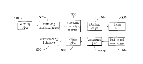
FIG. 1 is a flow chart of a method for manufacturing a light strip according
to
the present disclosure.
FIG. 2 is a schematic view of a winding rack wound with wires according to
the present disclosure.
FIG. 2A is a partially enlarged view of the winding rack according to the
present disclosure.
FIG. 2B is a sectional view of the winding rack according to the present
disclosure.
FIG. 3 is a schematic view of removing an insulation layer according to the
present disclosure.
2
CA 3013375 2018-08-03
FIG. 4 is a top view of the wires after the removal of the insulation layer
according to the present disclosure.
FIG. 5 is a schematic view of spreading a conductive material according to the
present disclosure.
FIG. 6 is a schematic view of attaching a chip according to the present
disclosure.
FIG. 7 is a schematic view of fixing the chip according to the present
disclosure.
FIG. 8 is a schematic view of dispensing glue according to the present
disclosure.
FIG. 9 is a schematic view of the winding rack and a carrier according to the
present disclosure.
FIG. 10 is a sectional view of a winding rack combination according to the
present disclosure.
FIG. 11 is a schematic view of a solder paste groove seat according to the
present disclosure.
FIG. 12 is a sectional view of another winding rack combination according to
the present disclosure.
DETAILED DESCRIPTION OF THE EXEMPLARY EMBODIMENTS
FIG. 1 is a flow chart of a method for manufacturing a light strip according
to
the present disclosure. The method of the present disclosure includes the
steps of:
winding a plurality of wires S10, removing an insulation layer S20, spreading
a
conductive material S30, attaching chips S40, fixing the chips in position
S50, testing
and maintaining S60, dispensing glue S70, solidifying the glue S80 and
extracting the
light strip S90, which will be respectively described in detail in the
following.
Referring to FIG. 2 to FIG. 2B, a winding rack 10 is provided in the step of
winding a plurality of wires S10. A wire fixing portion 12 is formed at both
ends of
the winding rack 10. A hollow portion 14 is formed at the winding rack 10
along a
longitudinal direction of the winding rack 10. The winding rack 10 may be a
metal
component, such as but not limited to a metal component made of an aluminum
material extruded from aluminum, or may be made of a thermal plastic material.
The
3
CA 3013375 2018-08-03
hollow portion 14 may be a partially open groove.
As shown in FIG. 2 and FIG. 2B, regarding the winding rack 10 made of metal,
the winding rack 10 preferably has a plurality of anti-slip strips 15
configured around
the winding rack 10 and being able to slightly protrude from a surface of the
winding
rack 10, but not limited thereto, so as to prevent wires W1 and W2 from
slipping. The
anti-slip strips 15 may be, for example, rubber, plastic, and so on. In this
embodiment,
two of the anti-slip strips 15 are disposed opposite to each other at two
sides of the
hollow portion 14 of the winding rack 10, and partially exposed from the top
surface
of the winding rack 10. In the present disclosure, the term "exposed from" may
include the meaning of "protruding from". Preferably, the anti-slip strips 15
are
replaceably configured on the winding rack 10.
In FIG. 2, the plurality of the wires W1 and W2 are wound around the winding
rack 10 in a plurality of coils so that the wires W1 and W2 extend repeatedly
across
the hollow portion 14. During the winding process, the ends of the wires WI
and W2
are fixedly wound to the wire fixing portion 12. In FIG. 2A, the wire fixing
portion 12
includes a concave portion 120 and a winding pin 123. The concave portion 120
is
formed at an end of the winding rack 10, and the winding pin 123 is fixed in
the
concave portion 120, wherein an end of the wires WI and W2 is wound to the
winding
pin 123. Then, a motor M rotates the winding rack 10. The wires W1 and W2 may
be, for example, enameled wires, but are not limited thereto. Each of the
wires WI and
W2 has an insulation layer covered on the outside (the outer layer shown in
FIG. 2, not
labeled). When the wires W1 and W2 are the enameled wires, the insulation
layer of
each of the wires W1 and W2 can be an enamel covering. In this embodiment, the
two
wires WI and W2 are taken as an exemplary example, but the present disclosure
is not
limited thereto. The number of the wires may be two or more, depending on the
requirements of the light strip.
Referring to FIG. 3 and FIG. 4, in the step of removing an insulation layer in
S20, a part of the insulation layer is removed from each of the wires WI and
W2 along
the hollow portion 14 to expose core wires CI and C2. In FIG. 3, removal of
the
insulation layer may be performed by a laser light source L emitting a laser
ray to
radiate the plurality of the wires WI and W2 along the hollow portion 14.
Then, LED chips C are attached and fixed to the core wires Cl and C2 of the
4
CA 3013375 2018-08-03
wires W1 and W2, so that the LED chips C are fixedly connected to the wires W1
and
W2. Specifically, the process of attaching and fixing the LED chips C include
the
steps S30, S40 and S50.
Referring to FIG. 5, in the step of spreading a conductive material S30, a
conductive material S is coated on each of the core wires Cl and C2 exposed
from the
wires WI and W2. For example, with a combination of a screen plate 90 and a
scraper
92, the conductive material S can be coated at a preset position. The
conductive
material S may be a solder paste, a silver paste, a conductive paste and so
on, but is
not limited thereto. A practical example is given by using the solder paste as
the
conductive material S, and the specific steps are as follows. Referring to
FIG. 9, for
batch production, this embodiment preferably provides a carrier 100. The
plurality of
the winding racks 10 with the wires W1 and W2 wound thereon are fixed side by
side
to the carrier 100, the carrier 100 has a pair of positioning seats 102, each
of the
positioning seats 102 is formed with a plurality of insertion concaves 1020,
and two
ends of each of the winding racks 10 are respectively placed in the insertion
concaves
1020 to print the conductive material S on the wires WI and W2 in a printing
manner.
A pair of grips 103 can also be configured on two sides of the carrier 100.
Referring to FIG. 6, the plurality of the LED chips C are placed on the
conductive material S in the step of attaching the LED chips C. In this
embodiment,
chip placing positions where the insulated layers are removed from the wires
W1 and
W2 are obtained by visual determination, and the LED chips C are held and
moved by
a suction head 30 to the chip placing positions.
Referring to FIG. 7, in the step of fixing the chips in position S50, the
conductive material S is baked along the hollow portion 14 of the winding rack
10 at a
predetermined temperature so that tin powder in the conductive material S is
melted to
fixedly connect the LED chips C to the wires W1 and W2. In this embodiment,
the
step of fixing the chips includes baking the positions where the LED chips C
are
disposed by a hot air device H along the hollow portion 14.
A purpose of the step of testing and maintaining S60 is to inspect whether the
LED chips C are able to emit light by being electrically connected to the
wires WI and
W2, before being fixedly welded. If the LED chips C fail to emit light, they
should be
checked and replaced.
5
CA 3013375 2018-08-03
In the step of dispensing glue S70, referring to FIG. 8, the LED chip C is
covered by a glue g with a glue gun G.
In the step of solidifying the glue S80, the glue g is usually solidified by
baking
with, for example, an oven.
In the step of extracting the light strip S90, the plurality of the wires W1
and
W2 are unwound from the winding rack 10.
Referring to FIG. 10 and FIG. 11, in the method for manufacturing the light
strip of the present disclosure, besides having cross sections that are
substantially the
same along a longitudinal direction, the winding rack 10 has a top surface, a
hollow
portion 14 along the longitudinal direction, and a plurality of anti-slip
strips 15
configured around the winding rack 10 and partially exposed from the top
surface.
Further, the present disclosure provides a winding rack 10 for manufacturing
the light
strip having relevant auxiliary elements. The winding rack 10 further has a
top wire
seat 20 and an outer seat 30. The top wire seat 20 is movably inserted in the
winding
rack 10, the winding rack 10 is placed in the outer seat 30, the top wire seat
20
includes a bottom 21 and a protrusion 22 protruding upward from the bottom 21,
the
bottom 21 of the top wire seat 20 has a bottom pad 28, and a wire groove 220
can be
formed on the top surface of the top wire seat 20 to fix the wires W1 and W2
in
position so as to prevent slippage. A depth of the wire groove 220 is smaller
than the
diameter of the wires WI and W2, and the wires W1 and W2 can be slightly
exposed
from the top surface of the top wire seat 20.
FIG. 11 shows another way of coating the conductive material. A solder paste
groove seat 95 is provided, and the winding rack 10 is inverted to coat the
conductive
material S on the wires WI and W2.
As shown in FIG. 12, a winding rack 10a has a plurality of insertion portions
17a and 17b, and a bottom 21a of a top wire seat 20a can be inserted into the
different
insertion portions 17a and 17b such that the length of winding the wires W1
and W2
would be different, namely, a circumference of the wires WI and W2 would be
different. Accordingly, the chip placing positions of the LED chips can be
adjusted to
manufacture a light strip having the LED chips with different spacing.
The feature of the present disclosure is that the LED light strip can be
automatically manufactured to lower the costs associated therewith.
6
CA 3013375 2018-08-03
The foregoing description of the exemplary embodiments of the disclosure has
been presented only for the purposes of illustration and description and is
not intended
to be exhaustive or to limit the disclosure to the precise forms disclosed.
Many
modifications and variations are possible in light of the above teaching.
The embodiments were chosen and described in order to explain the principles
of the disclosure and their practical application so as to enable others
skilled in the art
to utilize the disclosure and various embodiments and with various
modifications as
are suited to the particular use contemplated. Alternative embodiments will
become
apparent to those skilled in the art to which the present disclosure pertains
without
departing from its spirit and scope.
7
CA 3013375 2018-08-03