Note: Descriptions are shown in the official language in which they were submitted.
CA 03014085 2018-08-09
WO 2017/136951
PCT/CA2017/050164
THERMAL TREATMENT FOR PRECONDITIONING OR RESTORATION OF A SOLDER
JOINT
TECHNICAL FIELD
[0001] The following relates to systems and methods for soldering, and in
particular to a
thermal treatment operation which is applied for preconditioning and/or
restoration of a
solder joint.
DESCRIPTION OF THE RELATED ART
[0001] Historically, lead (Pb) containing solders, for example, tin-lead
(Sn-Pb)
solders, were used in the manufacture of electronics. However, lead and many
lead alloys
are toxic. Due to increasingly strict worldwide environmental regulations,
lead solders are
increasingly being replaced with less toxic lead-free solder counterparts that
also exhibit low
melting points and sufficient conductivity for electronics applications.
[0002] Lead-free solders containing alloys of tin (Sn) with silver (Ag)
and/or copper
(Cu) have been adopted by industry to replace the lead-containing solders. SAC
305 is an
example of a tin-silver-copper alloy solder that is widely used in industry.
The composition of
SAC305 is 96.5% tin, 3% silver and 0.5% copper.
[0003] It is commonly known that the solder properties of both Sn-Pb alloys
and their
replacement Sn-Ag-Cu alloys, such as SAC305, degrade over time. The primary
reason for
property degradation in Sn-Pb solder is grain growth, whereas in SAC305, the
second phase
(intermetallic) coarsening results in degradation of the solder properties
over time.
[0004] Early lead free solders typically required processing temperatures
higher than
those historically used for production with tin-lead solders. These early lead-
free solders
therefore required the use of specialized circuit board materials that could
withstand the
higher temperatures. Lead-free solders comprising alloys of tin (Sn), silver
(Ag), copper (Cu)
and bismuth (Bi) have been developed for low-temperature solder applications
that do not
require specialized circuit board materials. Examples of such low temperature
lead free
solders are described in US 2015/0258636. It has been found that individual
lead-free solder
joints formed using these alloys are typically composed of a few or even only
one Sn-rich
grain. As a result, failure of the solder joint may result when cleavage by
crack propagation
along the grain boundary occurs in response to impact or stress accumulation
on the joint.
Therefore, the typical grain structure of solder joints formed from tin,
silver, copper and
bismuth alloys results in unpredictable electronic solder joint reliability,
with a wide
distribution of lifetimes in the field.
- 1 -
CA 03014085 2018-08-09
WO 2017/136951
PCT/CA2017/050164
[0005] Another problem encountered with lead-free solder joints formed
using alloys of
tin, silver, copper and bismuth is that the Bi particles are unevenly
distributed in the
microstructure. The failure mechanism described above, of cleavage by crack
propagation
along a grain in response to impact or stress accumulation in the joint, is
exacerbated by the
brittleness of the precipitates.
[0006] The failure mechanisms resulting from the few large Sn grains and
the uneven
distribution of Bi particles may be summarized as failure due to unreliable
solder joints
caused by segregation of large, hard Bi and intermetallic compound (IMC)
particles around
unidirectional anisotropic Sn grains. The deformation behavior of as-cast lead-
free solder
joints in relation to grain size and orientation is described by Tae-Jyu Lee,
Bieler and Arfaei.
(Tae-Kyu Lee, Bite Zhou, Lauren Blair, Kuo-Chuan Liu, and Thomas R. Bieler, Sn-
Ag-Cu
Solder Joint Microstructure and Orientation Evolution as a Function of
Position and Thermal
Cycles in Ball Grid Arrays Using Orientation Imaging Microscopy, Journal of
Electronic
Materials, DOI: 10.1007/s11664-010-1348-4, 2010 TMS; R. J. Coyle, K. Sweatman
and B.
Arfaei, Thermal Fatigue Evaluation of Pb-Free Solder Joints: Results, Lessons
Learned, and
Future Trends, JOM, October 2015.)
[0007] It is possible to increase the number of grains of Sn in lead-free
electronic solder
joints through the use of aluminum (Al) as an additional alloying element. The
alloys with Al
have a trend to nucleate more Sn grains. However, the structure still consists
of a low
number of grains compared to Sn-Pb isotropic solder joints. Over E. Anderson,
Jason W.
Walleser, Joel L. Harringa, Fran Laabs and Alfred Kracher, Nucleation Control
and Thermal
Aging Resistance of Near-Eutectic Sn-Ag-Cu-X Solder Joints by Alloy Design,
Journal of
Electronic Materials, Vol. 38, No. 12, 2009.) Therefore, alternative solutions
to the problem
of the number of Sn grains are still needed.
[0008] The segregation of Bi particles and the impact of this phenomenon on
solder
joint reliability have not yet attracted significant research attention.
Therefore, solutions to
this problem are needed.
[0009] Annealing of lead-tin and lead-tin-antimony solders to improve
solder stability is
described by B.T. Lampe; "Room Temperature Aging Properties of Some Solder
Alloys
Welding Research Supplement," October 1976; p330-340 ("Lampe"). Lampe
describes
changes in the microstructure observed in the lead-containing alloys over a
period of aging
at room temperature, and found that heating at 200 F could produce similar
characteristics
in a tin-lead-antimony alloy, but at a faster rate. Lampe also found that the
annealing at
200QF resulted in a somewhat higher shear strength and hardness in the final
stabilized
product.
- 2 -
CA 03014085 2018-08-09
WO 2017/136951
PCT/CA2017/050164
[0010] In another study, heat treatment is used to artificially accelerate
aging of solder
alloys to study the properties of the solder alloys and to predict field
behavior over time. In
mainstream applications of Sn-based Pb-free solder, properties such as
hardness and
number of thermal cycles to failure degrade overtime. This property
degradation is caused
by microstructure degradation related to the second phase particles coarsening
as described
by T. K. Lee. (Tae-Kyu Lee, Hongtao Ma, Kuo-Chuan Liu and Jie Xue, Impact of
Isothermal
Aging on Long-Term Reliability of Fine-Pitch Ball Grid Array Packages with Sn-
Ag-Cu Solder
Interconnects: Surface Finish Effects, Journal of Electronic Materials, Vol.
39, No. 12, 2010.)
[0011] Beneficial changes in the microstructure of Sn-Zn-Cu alloys by
annealing at
elevated temperatures for extended time periods was reported by Klasik. (A.
Klasik et al.
"Relationship Between Mechanical Properties of Lead-Free Solder and Their Heat
Treatment Parameters" Journal of Materials Engineering and Performance, vol.
21(5) May
2012, p620-628.) These microstructural changes, observed after heating at
elevated
temperatures for time periods of from 168 to 24 hours, result in the
improvement of the
mechanical strength.
SUMMARY
[0012] It has been found that solder joints (interconnects) in an assembly
can be
conditioned to improve the solder joint properties. In one aspect the
conditioning treatment
can improve the solder joint properties by the formation of smaller bismuth
particles that are
more evenly distributed in the solder joint.
[0013] In one aspect there is provided a method for conditioning a solder
joint
comprising:
- i) obtaining an assembly having a solder joint wherein the
solder
joint is a lead free solder joint comprising Bi and Sn and
- ii) heating the assembly to a temperature near the solvus
temperature of the alloy,
- wherein when the assembly has cooled the bismuth particles are
smaller and more evenly distributed in the solder joint that before the
heating step.
[0014] In an embodiment of the method the lead free solder joint comprises
at least 2
weight percent of Bi. In another embodiment the lead free solder joint further
includes Ag
and/or Cu. The balance or remainder of the lead free solder joint is Sn.
- 3 -
CA 03014085 2018-08-09
WO 2017/136951
PCT/CA2017/050164
[0015] In another embodiment of the method, the step of heating the
assembly to a
temperature near the solvus temperature involves heating the assembly to a
temperature in
the range of up to 15 degrees Celsius below the solvus temperature and up to
40 degrees
Celcius above the solvus temperature. The solvus temperature for a solder
composition
may be experimentally determined by methods known in the art, for example,
DSC.
[0016] Conditioning of the solder joint may occur as part of the initial
manufacturing
process or may take place after a period of use of the assembly under field
conditions. In
the case where the conditioning occurs during the manufacturing process
(preconditioning)
the conditioning step will occur at a point after the step of reflow to form
the solder joint and
before the assembly is used in the field. Other processing or testing steps
may occur in the
manufacturing process before or after the conditioning step. In the case where
the
conditioning occurs after the use of the assembly under field conditions
(restoration or
reconditioning) the assembly will have had some period of use before the
conditioning
process is applied. The period of use will depend on factors such as the type
of solder, the
application that the assembly is used for, and the environment where it is
used.
[0017] In another aspect there is provided a process for preparing an
electronic
assembly comprising:
a) depositing a lead-free bismuth containing solder paste
b) placing surface mount components
c) forming solder joints (interconnects) by reflow and/or wave soldering
and
d) conditioning the lead-free bismuth containing solder joint by the
method as described herein.
BRIEF DESCRIPTION OF THE DRAWINGS
[0018] Embodiments will now be described by way of example only with
reference to
the appended drawings wherein:
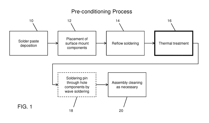
[0019] FIG. 1 is a flow diagram illustrating a soldering process with a
thermal treatment
step applied as a preconditioning operation;
[0020] FIG. 2 is a flow diagram illustrating a thermal treatment step
applied as a
restoration operation to a previously soldered joint;
[0021] FIG. 3 is a polarized light image showing Sn grains in an
interconnect (solder
joint);
- 4 -
CA 03014085 2018-08-09
WO 2017/136951
PCT/CA2017/050164
[0022] FIG. 4 is a polarized light image of lead free solder
interconnects in a 14x14 ball
grid array (BGA);
[0023] FIG. 5 is a SEM image of a lead-free solder joint
showing uneven distribution of
Bi particles;
[0024] FIG. 6 is a SEM image of grain microstructures in a
lead-free solder interconnect
after a standard reflow process;
[0025] FIG. 7 is a SEM image of grain microstructure in a
lead-free solder interconnect
after a thermal treatment following the standard reflow process;
[0026] FIG. 8 is an electron backscatter diffraction (EBSD)
analysis of the image of FIG.
6;
[0027] FIG. 9 is an EBSD analysis of the image of FIG. 7;
[0028] FIG. 10 is a graph showing the solvus temperature
curve for SnBi compounds,
the Y axis showing temperature in degrees Celsius and the X axis showing
increasing
percent Bi from left to right, with 0% Bi and 100% Sn at left with the
experimentally
determined solvus temperatures for specific compositions plotted on the graph;
[0029] FIG. 11 is a bar graph depicting hardness after aging
at room temperature for a
specific number of days as shown in the legend;
[0030] FIG. 12 is a bar graph depicting hardness after aging
at 100 C for a specific
number of days as shown in the legend;
[0031] FIG. 13 includes SEM images of microstructure changes
over time with heating
at 1250C;
[0032] FIG. 14 is a schematic showing microstructural changes
during thermal
treatment: Bi dissolution at high temperature, new grain formation and small
particles of Bi
precipitation at the cooling stage;
[0033] FIG. 15 is an SEM image showing Bi pinning of grain
boundaries in a SnAgCuBi
alloy;
[0034] FIG 16 is an SEM image showing microstructure changes
with temperature
cycling in a SnAgCuBi alloy;
[0035] FIG 17 is an SEM image showing microstructure in a
SnAgCuBi alloy coarsened
after aging;
- 5 -
1
CA 03014085 2018-08-09
WO 2017/136951 PCT/CA
2017/050164
[0036] FIG 18 is an SEM image showing microstructure changes after a
restoration
treatment in a SnAgCuBi alloy.
[0037] Figure 19 is a graph depicting creep rate changes after aging at 70
C for a
specific number of days and after thermal treatment as shown in the legend.
[0038] Figure 20 is a graph showing DSC scans of a composition of Sn /
0.7%Cu /
7%Bi.
DETAILED DESCRIPTION
[0039] The following relates generally to soldering processes and more
specifically to
lead-free solder containing bismuth. As described below, it has been found
that a thermal
treatment or processing operation can be applied to such solders to create a
more reliable
grain-refined solder joint with an even distribution of bismuth across the
solder joint. The
thermal treatment step can be incorporated into electronic assembly
manufacturing, e.g., of
circuit boards having soldered components.
[0040] As is known in the art, a standard electronics assembly soldering
process
includes the following steps, which have been implemented in various
applications for a long
period of time:
a) solder paste deposition by printing;
b) placement of surface mount components;
C) reflow soldering (melting of printed solder in an oven and solder joint
formation)
d) if applicable, soldering of pin through hole components by "wave" solder in
a pot; and
e) assembly cleaning as necessary.
[0041] It has been determined that for lead-free solders containing
bismuth, an
additional thermal treatment step can be applied after the initial solder
joint formation step,
known as reflow, to improve the solder joint properties. FIG. 1 illustrates
the above process
with the inclusion of this additional thermal treatment step. This thermal
treatment step,
which may also be referred to herein as "preconditioning", creates a more
reliable grain-
refined solder joint with a more even distribution of Bi across the solder
joint. The thermal
treatment may be combined with other assembly-level thermal treatments such as
curing of
conformal coating or high operating temperature burn-in. As such, the
particular
embodiment shown in FIG. 1 is for illustrative purposes only. The pre-
conditioning step may
- 6 -
CA 03014085 2018-08-09
WO 2017/136951
PCT/CA2017/050164
take place before or after other processing steps which occur after reflow.
The pre-
conditioning step will take place before the assembly is used in the field.
[0042] In the process exemplified in FIG. 1, solder paste deposition is
applied to the
circuit board at step 10 and surface mount components are placed on the board
at step 12.
Reflow soldering is then performed at step 14, which includes heating the
board to melt the
solder paste and thus form the solder joint with the leads of the component
that have been
aligned with the solder paste. The thermal treatment step 16 is applied after
the solder
reflow step at 14 to improve the solder joints as will be described in greater
detail below.
Step 18 includes soldering pin through hole components, if applicable (as
illustrated in
dashed lines), to the board. This normally includes a wave soldering process
using a pot
wherein a wave of molten solder comes into contact with the through hole
locations on the
board as it passes over the pot to solder the through hole pins to the board.
Some assembly
cleaning may be necessary at step 20, as is known in the art. This step may
include a visual
inspection of the soldered joints (manual or machine) as well as various other
quality control
measures.
[0043] It has also been found that the principles described herein can also
be used for
the restoration of acceptable solder joint properties after a period of time
and possible use
has elapsed. For example, restoration may be done after several years of
product service. A
similar thermal treatment step can be applied to a previously prepared solder
joint containing
a lead-free bismuth containing alloy. The thermal treatment step applied for
"restoration"
can be used to restore a more reliable grain-refined solder joint with even
distribution of Bi
across the solder joint, as part of a restoration and refurbishment process,
after the solder
interconnect structure has coarsened over time in service. FIG. 2 illustrates
an example of
an application for applying the heat treatment step 16 to a previously
soldered board that
has been in use for a period of time. A board to be restored is obtained at
step 30 and the
thermal treatment step 16 applied to one or more components on the board. A
cool down
step 34 is also applied, in which new small particles precipitate evenly in
the matrix, to
improve thermomechanical properties as discussed in greater detail below. A
preferred time
for the restoration of field products may be estimated either from historical
data collected for
products used in the field or by estimation of the effect of diffusion rates
of Bi in the solder at
the field conditions.
[0044] In a particular aspect the particles of Bismuth in a bismuth
containing lead-free
solder joint after conditioning treatment will be smaller and more evenly
distributed than the
particles before conditioning.
- 7 -
CA 03014085 2018-08-09
WO 2017/136951
PCT/CA2017/050164
[0045] In a particular embodiment, the lead-free solder alloy containing
bismuth further
contains tin. In still a further embodiment the solder alloy includes one or
more of silver and
copper. In a further embodiment, the solder has a bismuth concentration
between about 1
and about 10 weight percent. In a further embodiment the bismuth concentration
is equal to
or greater than 2 weight percent. In a particular embodiment, the bismuth
concentration is
between about 2 and about 7 weight percent. In another embodiment, the
composition of
lead-free bismuth containing solder has from 0 to 5% Ag, 0 to 1% Cu and 1 to
10% Bi with
the remainder being Sn (percentages are weight percent). In a further
embodiment the
composition of lead-free bismuth containing solder has from >0 to 5% Ag, >0 to
1% Cu and
from about 2 to 7% Bi with the remainder being Sn (percentages are weight
percent).
[0046] The term "pinning" as used herein refers to the action of a point
defect which
may be a second phase precipitate in a material which acts as a barrier to
movement of a
dislocation in the crystal structure.
[0047] The term "intermetallic compound" or "IMC" is a solid-state compound
exhibiting
metallic bonding, defined stoichiometry and ordered crystal structure.
[0048] The term "creep" or "creep rate" as used herein means the tendency
of
a solid material to move slowly or deform permanently under the influence of
mechanical stresses, and is measured by techniques such as nano-indentation.
[0049] The thermal treatment step 16 is described in more detail below,
making
reference to FIGS. 3 through 16.
[0050] It is generally known that solder interconnects with desirable
mechanical
properties can be achieved by using a material having a homogeneous structure
with small
grains of ductile matrix and an evenly distributed second phase pinning the
grain
boundaries. These features strengthen the solder material by acting as a
barrier which
prevents a dislocation which may occur in the material from traveling through
a lattice when
a relatively small stress is applied.
[0051] It has been recognized that individual lead-free solder
interconnects (solder
joints) are typically composed of a few or even only one Sn-rich grain. FIG. 3
is an SEM
image which shows 3 grains in one ball grid array (BGA) interconnect. In FIG.
4, a polarized
light image of a 14x14 BGA is provided which shows single crystals with only a
few crystal
orientations with each joint having a different orientation.
[0052] The method of conditioning and in particular thermal treatment step
16
described herein is aimed at converting the as-cast microstructure of the lead-
free bismuth-
containing alloys having large Sn dendrites (one or several grains in a solder
joint) and
- 8 -
CA 03014085 2018-08-09
WO 2017/136951
PCT/CA2017/050164
segregated, relatively large Bi particles in the interdendritic spaces, into
the desired more
reliable structure having many small Sn grains and more evenly distributed Bi
particles.
[0053] The overall performance of lead-free solder interconnects is
dictated by the
properties of p-Sn, which exhibits a significant anisotropic nature due to its
special body-
centered tetragonal (BCT) crystal structure with lattice parameters of a =
0.5632 nm, c --
0.3182 nm, and c/a = 0.547. Therefore, the small number of grains in an
interconnect and
the significant inherent anisotropic nature of the thermomechanical properties
of p-Sn make
Pb-free solder interconnects behave differently from their Sn-Pb counterparts,
and the
crystallographic orientation of each individual grain plays a very important
role in dictating
the overall thermomechanical performance. The stress state and strain history
of every joint
is different, because the orientation and boundary conditions are different.
[0054] These anisotropic interconnects can result in at worst,
unpredictable
performance, and at best, electronic solder joint reliability with a wide
distribution of lifetimes
in the field. The specific failure mechanism that is known to occur is early
life solder joint
cleavage by crack propagation along a grain in response to impact or stress
accumulation in
the joint.
[0055] It has also been recognized that after solidification of a lead-free
bismuth-
containing solder joint, the Bi particles are unevenly distributed in the
microstructure as
illustrated in FIG. 5. The Bi particles precipitate from the Sn matrix
predominately between
the Sn dendritic arms and in interdendritic spaces close to the intermetallic
particles such as
Ag3Sn and Cu6Sn5, solidifying from the last portion of liquid. The specific
failure mechanism
that occurs is early life solder joint cleavage by crack propagation along a
grain in response
to impact or stress accumulation in the joint, exacerbated by the brittleness
of the
precipitates.
[0056] The preconditioning and restoration treatments shown in FIGS. 1 and
2 can be
used to treat electronic solder assemblies with lead-free solder comprising
SnBi, Sn(Ag)Bi,
Sn(Cu)Bi or Sn(Ag)CuBi to advantageously achieve better properties for the
solder joints as
follows.
[0057] The thermal treatment step 16 is utilized to address the
aforementioned issue
with random crystal orientations and uneven microstructures. The thermal
treatment step 16
addresses this issue by obtaining a solder joint having many small randomly
oriented grains
with more uniformly distributed Bi particles. The resulting microstructure is
somewhat similar
to Sn-Pb.
- 9 -
I
CA 03014085 2018-08-09
WO 2017/136951
PCT/CA2017/050164
[0058] The recrystallization process can significantly change
the crystallographic
orientation and microstructure, and therefore, the mechanical properties of
the bismuth-
containing, lead-free solder interconnects.
[0059] According to the dispersion strengthening theory, the
presence of second-phase
particles can reinforce the solder matrix and inhibit the localized softening
and deformation in
the recrystallized region, improving the overall mechanical performance of
lead-free solder
interconnects.
[0060] The SEM image in FIG. 6 shows an example of the grain
structure after
standard reflow with a bismuth containing lead-free solder. The image shows
the large Bi
precipitate and uniaxial grain orientation (the corresponding grain
orientation is shown in
FIG. 8 using EBSD analysis). FIG. 7 shows the microstructure of the same
sample after
thermal treatment. The sample after the thermal treatment has small evenly
distributed Bi
particles in the Sn matrix with many differently oriented grains (the grain
orientation is shown
in FIG. 9 using EBSD analysis).
[0061] FIG. 8 shows the grain structure after standard
reflow, with large Bi precipitate
(more readily visible in FIG. 6) and uniaxial grain orientation. FIG. 9 shows
the
microstructure after thermal treatment, with small evenly distributed Bi
particles in Sn matrix
(more easily visible in FIG. 7), with many differently oriented grains. The
microstructures
shown in the images of FIGS. 6 through 9 are of interconnects formed using the
Violet alloy
having the composition Sn / 2.25 /0Ag / 0.5%Cu / 6%Bi, wherein the percentages
are weight
percentages and the Sn forms the balance of the composition. FIGS. 6 and 8 are
images
taken after reflow and solidification, while FIGS. 7 and 9 are images taken
after a
conditioning treatment comprising heating the sample for 50 hours at 125 C
then allowing
the sample to cool, following the original reflow and solidification process.
[0062] Table 1 shows the compositions of a variety of alloys
that were investigated
indicating the percent weight of the components. Where the percentage of Sn is
not defined
in the composition, Sn is assumed to make up the balance of the composition.
SnPb and
SAC305 were used as standards for comparison. Different thermal treatments
were
performed on the alloy compositions both above the temperature of Bi
dissolution in Sn
(above solvus) and below the temperature of Bi dissolution in Sn (below
solvus). The solvus
temperature for each alloy containing Bi was experimentally determined using
DSC
(differential scanning calorimetry) and microstructural analysis. By way of
example, FIG. 20
shows a graph of DSC scans obtained for the Sunflower composition. FIG. 10
illustrates a
solvus temperatures curve for compositions of Sn and Bi, with the Y axis
showing the
change in temperature in degrees celsius and the X axis showing increasing
percentage of
-10-
i
CA 03014085 2018-08-09
WO 2017/136951 PCT/CA2017/050164
Bi from left to right; with 100% Sn at the left. The portion of the curve
displayed in FIG. 10 is
the tin rich portion of the phase diagram shown in FIG. 14. The experimentally
determined
solvus temperatures for the compositions Senju, Violet and Sunflower (defined
in Table 1)
are plotted on the solvus curve shown in FIG. 10.
Table 1: Alloys Investigated
Alloy number Alloy Name Composition Comment
1 SnPb Sn /37%Pb = Baseline
2 SAC305 Sn / 3%Ag / 0.5%Cu = Pb-free Baseline
3 Senju M42 Sn / 2%Ag / 0.75%Cu / = Commercially
Available
3%Bi = Low Bi content
4 Violet Sn / 2.25%Ag / 0.5%Cu / = Performed well in vibration
6%Bi and thermal cycling
Screening Test
Sunflower Sn / 0.7%Cu / 7%Bi = No Ag
= Lower cost alternative
[0063] Table 2 describes the thermal treatment parameters applied to
various soldering
alloys; the compositions of the alloys tested are defined in Table 1. (The "+"
symbol
indicates that the alloy has been tested under the condition described in the
left hand
columns.) The solvus line for the lead-free alloys can be found in FIG. 10.
Table 2: Experimental Parameters for Thermal Treatments
Name of Treatmen Parameters tested Alloys (from Table
1)
thermal t #
treatment
Temp, C Time, cycles 4 5 3 2 1
hours
Annealing 1 125 2,4,8 N/A .. +
pre- 16, 24,
conditioning 50, 100,
200
2 75 2,4,8 N/A
16, 24,
50, 100,
200
-11-
CA 03014085 2018-08-09
WO 2017/136951
PCT/CA2017/050164
3 25 24,50, N/A
100,
200,
1000,
2000,
6000
Cycling pre- 4 125 0.1, 0.5, 2
conditioning 2, 8
75 0.1,0.5, 8
2,8
Annealing 6 120, 125 8, 24 N/A
restoration
after 70 C
300 hours
Annealing 7 125 8, 24 N/A
restoration
after 25 C
2000 hours
Cycling 8 125 0.1, 0.5 2, 8
restoration
after 75 C
300 hours
Cycling 9 125 0.1, 0.5 2, 8
restoration
after 25 C
2000 hours
[0064] Data from the experiments described in Table 2 have shown that the
desirable
results of grain refinement and more even distribution of small Bi particles
may be achieved
by heating the alloys above solvus or to a temperature in the proximity of
solvus. The
experimental data showed that with exposure for more than 24 hours at
temperatures above
solvus or with exposure for 100 hours or more at temperatures below solvus
good results in
terms of grain refinement and more even distribution of small Bi particles is
achieved.
[0065] It has been found that by employing multiple cycles of heating and
cooling, the
amount of time required to achieve the desired results of grain refinement and
more even Bi
particle distribution can be dramatically reduced. While experimental trials
using as many as
8 heating cycles were carried out, it was found that even using as few as two
cycles with 10
-12-
1
CA 03014085 2018-08-09
WO 2017/136951 PCT/CA
2017/050164
minutes dwell at a temperature above solvus results in a structure with small
grains with
different orientation.
[0066] Accordingly, a thermal treatment method has been
discovered that can improve
solder joints made from Pb-free alloys containing Bi. In a particular
embodiment the heating
temperature will be a temperature on or near the solvus line for the
composition. A
temperature near the solvus temperature may include temperatures up to about
15 C below
the solvus, up to 10 C below the solvus or up to 5 C below the solvus. In a
further
embodiment, a temperature near the solvus may include temperatures up to about
40 C
above the solvus, up to about 30 C above the solvus temperature, up to 20 C
above the
solvus, up to 10 C above the solvus or up to 5 C above the solvus.
[0067] In a further aspect the Pb-free bismuth containing
alloy is an alloy comprising at
least 2%Bi by weight. In yet another aspect the alloy has from about 0 to
about 5% Ag,
about 0 to about 1% Cu and about 1 to about 10% Bi with the remainder being Sn
(percentages are weight percent). In a further embodiment the composition of
lead-free
bismuth containing solder has from >0 to about 5% Ag, >0 to about 1% Cu and
from about 2
to about 7% Bi with the remainder being Sn (percentages are weight percent).
[0068] In still a further aspect the temperature for the
thermal treatment whether for
annealing or cyclic treatment will be selected such that it does not exceed a
temperature
which would damage other aspects of the circuit board of which the solder
forms a part
during the selected time duration of the heating.
[0069] In a particular aspect the thermal treatment step 16
includes the following
additional sub-steps after the reflow:
(1) Heating an electronic assembly to a temperature near the solvus of the
alloy
depending on the alloy used for the solder composition. For example for solder
compositions as shown in FIG. 10 and Table 3 the temperature may be in the
range
of 45-125 C.
(2) Thermal exposure of the interconnect to achieve full Bi particle
dissolution and
even distribution of subsequently precipitated Bi particles in Sn to approach
the r = 0
condition. Where in the r is the radius of the Bi particle and the radius of
the Bi
particle, r, is mathematically expressed as a function of the annealing time,
t, by the
parabolic relationship, r2 = Kt. The parabolic coefficient K is a function of
the
temperature, T, by an Arrhenius equation of K = Ko exp(-QIVRT), where R is the
gas
constant.
(3) Cooling down to ambient temperature for recrystallization and uniform Bi
particle
precipitation from a solid solution of Bi in Sn.
-13-
1
CA 03014085 2018-08-09
WO 2017/136951
PCT/CA2017/050164
Table 3: Experimentally determined solvus temperatures
Sample Sample Sample
Average Difference
Alloy 1 Peak 2 Peak 3 Peak
( C) ( C)
( C) ( C) ( C)
Sunflower
83 82 82.06 82
(Sn/0.7%Cu/7%Bi) 3
Sn/7%Bi 82 76 N/A 79
Violet
N/A 86 92 89
(Sn/2.25%Ag/0.5%Cu/6%Bi) 7
Sn/6%Bi 82 82 N/A 82
Senju
N/A N/A 42 42
(Sn/2%Ag/0.7%Cu/3%Bi) 6
Sn/3%Bi N/A N/A 36 36
[0070] The compositions are defined with respect to their weight
percentages with Sn
making up the balance of the composition.
[0071] Preconditioning may be done for several minutes or several hours and
up to
several days, in order to achieve full dissolution of the Bi particles and
even distribution of
the Bi across all grains in the solder joint. The time and temperature
duration is dependent
on the selected Bi-containing alloy. For example, Violet alloy requires up to
50 hours of
thermal treatment for full Bi dissolution. Pre-conditioning (or
reconditioning) under non-
optimized conditions, for example, at a temperature or for a time that is not
optimal may
result in partial dissolution which may also provide Bi particle size and/or
particle distribution
which is improved over samples that have not undergone a thermal treatment
step.
Preconditioning or reconditioning under non-optimized conditions may still
provide solder
interconnects having acceptable properties depending on the application.
[0072] In practice the time and temperature for the annealing or heat
cycling step may
be selected to provide suitable conditioning results and may also be adapted
or conformed
to other manufacturing requirements. For example, temperatures in a range from
about 25
C to about 180 C, from about 25 C to about 160 C, from about 25 C to about
130 C,
from about 75 C to about 180 C, from about 75 C to about 160 C, or from
about 75 C to
about 130 C may be used. In another example, the temperature may be 125 15 C
or
120 5 C. The time for a single step annealing process may, for example, range
from about
- 14-
CA 03014085 2018-08-09
WO 2017/136951
PCT/CA2017/050164
minutes to about 300 hours, from about 10 minutes to about 100 hours, from
about 10
minutes to about 50 hours, from about 10 minutes to about 24 hours, from about
2 hours to
about 50 hours or from about 2 hours to about 24 hours. The time duration for
one cycle of
a multicycle heating process may be from about 5 min to about 8 hours.
[0073] Solder joint recrystallization from anisotropically oriented large
grains to a grain
structure of many small grains isotropically oriented (non-oriented) has been
found to result
in improved solder joint reliability due to improved creep and fatigue
behaviour and improved
global modulus.
[0074] The interim indicator of solder joint improvement is hardness, which
is known to
correlate to solder joint reliability. In contrast to the SnAgCu (SAC) alloy,
which loses its
hardness over time at room and elevated temperature, alloys with Bi are stable
and keep
constant hardness under the same conditions.
[0075] It has been found therefore that alloys of Sn(Ag)CuBi, as shown in
FIGS. 11 and
12 increase or plateau in hardness with time. This illustrates the binary and
ternary alloy
behaviors with respect to Bi and Cu. In the bar graphs of FIGS. 11 and 12 the
Y axis shows
the hardness scale, Rockwell Superficial 15x, which refers to a superficial or
less deep
indent than standard, measured at a load of 15N where x represents the
diameter of the
indenter which was 1/4 inch.
[0076] The reliability of these alloys in this respect has already been
published. A
summary of the findings on the reliability studies of SnAgCuBi alloy can be
found in the
reference, Journal of Microelectronics and Electronic Packaging (2015) 12, 1-
29.
[0077] Bismuth containing alloys formed excellent joints on organic
solderability
preservative (OSP) finish. The interfacial intermetallic layer was comparable
to SnPb solders
in thickness and shape, and thinner than in SAC305. The solder composition
Sn2.25Ag0.5Cu6Bi (Violet), is compatible not only with OSP but also with
electroless nickel
immersion gold (ENIG) and electroless nickel electroless palladium immersion
gold
(ENEPIG), and forms excellent solder joints with uniform intermetallic layers
on both BGA
and leaded components.
[0078] All combinations of alloys tested (Paul (Sn3.4Ag4.8Bi) Violet,
Orchid
(Sn2Ag7Bi), SAC305, and SnPb), surface finishes (OSP, ENIG, and ENEPIG), and
board
laminate (normal and high glass transition (Tg)) passed the aerospace ATC
qualification
requirement of 1,000 cycles of 55 C to 125 C. There was no solder joint
failure on both
high gloss and normal Tg boards up to 3,010 cycles for Pb-free lower melt
(Paul, Violet, and
Orchid) and SAC305 alloys. All three experimental alloys (i.e., Paul, Violet,
and Orchid)
showed excellent performance in harsh-environment thermal cycling.
-15-
CA 03014085 2018-08-09
WO 2017/136951
PCT/CA2017/050164
[0079] The vibration failure analysis was based on 1 million cycles at 2G
and 5G, for
failures found by resistance monitoring. The lowest failure rate found was for
Violet at both
the 2-G and 5-G levels; the failure rates were better than for SnAgCu solder
alloys.
[0080] The microstructure improvement over time at 125 C is shown in FIG.
13. Small
equiaxial grains forming during Bi particles dissolution and Bi precipitation
on grain
boundaries (depicted in the schematic of FIG. 14) provide exceptional creep
and fatigue
resistance.
[0081] Currently the electronics industry standards governing the use of
soldering
materials focus on the use of approved solder metal alloys, acceptable
contaminant levels,
and appropriate flux materials under appropriate manufacturing conditions.
Specific process
parameters for high reliability are not addressed. The relevant electronic
industry IPC
standards are listed below.
[0082] The standards include IPC J-STD-001 Requirements for Soldered
Electrical and
Electronic Assemblies , J-STD-001xS Space Hardware Addendum, J-STD-004 , J-STD-
005
Requirements for Soldering Pastes, J-STD-006 Requirements for Electronic Grade
Solder
Alloys and Fluxed and Non-Fluxed Solid Solders for Electronic Soldering
Applications, IPC-
A-610 Acceptability of Electronic Assemblies, I PC/WHMA-A-620 Space Hardware
Addendum Space Applications Electronic Hardware Addendum for IPC/WHMA-A-620.]
[0083] The thermal process parameters for each material are different and
may be
experimentally determined and verified.
[0084] The thermal treatment process described above may be used in the
electronics
assembly manufacturing processes.
[0085] With respect to the application of the thermal treatment step 16 to
restoration, it
has also been recognized that lead-free solder interconnect microstructures
experience
coarsening over time. Sn grain size increases and Bi or other precipitants get
bigger and
form solid rims around grain boundaries. These properties are degrading to the
function of
the solder joint.
[0086] The thermal treatment step 16 allows one to restore the
microstructure and
properties of lead-free alloys with solid solution and precipitation
hardening.
[0087] Heating the assembly to a temperature near the solvus, allows Bi
particles to be
dissolved in Sn. For example, the assembly can be heated to about 652 to 100
C, for about
15 to 30 min. Following the heating step, the material is allowed to cool.
During cooling,
new small particles will precipitate evenly in the Sn matrix, which will
improve
thermomechanical properties.
[0088] Further evidence of the improvement of mechanical properties by the
conditioning treatment after aging in the field is provided by creep rate
experimental data.
-16-
I
CA 03014085 2018-08-09
WO 2017/136951
PCT/CA2017/050164
FIG. 19 shows the creep rate after aging for Violet alloy (defined above)
compared to SAC.
Aging was simulated by 300 hours baking of solder joints below solvus at 70 C.
A 24 hour
treatment of aged samples at 120 C was enough to provide a significant
improvement in
creep resistance. In this experiment with Violet alloy, additional treatments
at higher
temperatures of, for example 120 C for up to 300 hours did not show a
significant additional
benefit. However, additional treatment at higher temperatures and longer time
periods may
provide some additional benefit which in may be significant in certain
instances.
[0089] For simplicity and clarity of illustration, where
considered appropriate, reference
numerals may be repeated among the figures to indicate corresponding or
analogous
elements. In addition, numerous specific details are set forth in order to
provide a thorough
understanding of the examples described herein. However, it will be understood
by those of
ordinary skill in the art that the examples described herein may be practiced
without these
specific details. In other instances, well-known methods, procedures and
components have
not been described in detail so as not to obscure the examples described
herein. Also, the
description is not to be considered as limiting the scope of the examples
described herein.
[0090] It will be appreciated that the examples and
corresponding diagrams used herein
are for illustrative purposes only. Different configurations and terminology
can be used
without departing from the principles expressed herein.
[0091] The steps or operations in the flow charts and
diagrams described herein are just
for example. There may be many variations to these steps or operations without
departing
from the principles discussed above. For instance, the steps may be performed
in a differing
order, or steps may be added, deleted, or modified.
[0092] Although the above principles have been described with
reference to certain
specific examples, various modifications thereof will be apparent to those
skilled in the art as
outlined in the appended claims.
[0093] The disclosures of all prior art recited or described
herein are hereby
incorporated by reference in their entirety.
-17-
i