Note: Descriptions are shown in the official language in which they were submitted.
TECHNIQUES FOR LASER ALIGNMENT IN PHOTONIC INTEGRATED
CIRCUITS
FIELD OF THE DISCLOSURE
[0001] The present disclosure relates generally to semiconductor lasers
and, more
particularly, to techniques for aligning semiconductor lasers to a Photonic
Integrated Circuit
(PIC) substrate.
BACKGROUND OF THE DISCLOSURE
[0002] Silicon photonics chips require electric current and light to be
applied in order to
function. The electric current is provided in a similar fashion to that used
with other types of
silicon chips. However, various approaches have been used, thus far, to
provide the light
input to PIC substrates to foiiii a PIC. The main approach used for optical
coupling is based
on active alignment. Using active alignment, light may be generated by
powering a laser,
energy from which is typically detected downstream. To peak optical coupling,
the laser,
fiber, lens, or other intermediate objects are precisely moved relative to the
detector before
fixing the geometry. This approach requires electrical contact to the laser
early in the
assembly process, which can complicate manufacturability. Below are three
examples of light
coupling to PIC substrates.
[0003] A first example uses an optical fiber that brings light to a PIC
substrate. This
example uses active alignment of the optical fiber to the PIC substrate, which
can be time-
consuming and expensive and can produce fragile assembly. Using optical fiber
also
consumes a large amount of space not just for the fiber, but also for a
packaged
semiconductor laser that may be connected to the other end of the optical
fiber.
[0004] A second example uses an externally packaged semiconductor laser
diode with a
lens and other optical elements, as disclosed in US Patent 8,168,939. Although
this example
reduces an amount of space used compared to the first example, it still
consumes too much
space, as well as adds costs associated with the optical elements and required
assembly and
packaging. This example also typically requires activation of the laser during
alignment.
[0005] A third example uses a cleaved or etched facet semiconductor laser
directly with a
silicon photonics chip. This example minimizes overall size, however, it
requires either
active or passive alignment of the semiconductor laser to the silicon
photonics chip, which
are time-consuming and add cost.
[0006] To address the above shortcomings, some effort has been placed on
using passive
alignment to reduce cost and speed assembly. In passive alignment, optical
fiducials on parts
1
Date Recue/Date Received 2023-04-17
are typically viewed with a microscope imaging system, and the parts are then
simply mated
and fixed without measuring the optical coupling performance. Passive
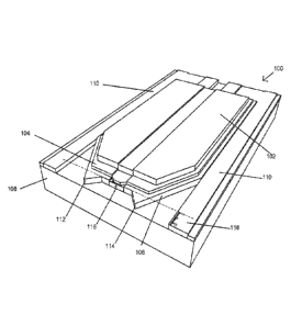
alignment can be
simple and quick, but is severely limited by the cost and time required to
achieve needed
precision. Resulting alignment precision below 15 microns is prohibitively
expensive.
[0007] The above challenges and shortcomings associated with current
delivery of light
to PIC substrates have hindered the ability to use PICs in a beneficial way in
applications
such as data center connectivity.
SUMMARY OF THE DISCLOSURE
[0008] In some embodiments, a photonic integrated circuit (PIC) comprises a
semiconductor laser including a forward guide surface and a PIC substrate
including a mated
surface, wherein the semiconductor laser is aligned in the PIC substrate by
placing the
semiconductor laser in the PIC substrate and mating the forward guide surface
to the mated
surface. The guide surfaces may have different shapes, such as triangles or
clipped triangles.
The mated surface may match the shape of the guide surface, or may contain
relief from the
guide surface. The mated surface may contain a curved edge. The semiconductor
laser and
the PIC substrate may contain rulers etched into the substrate to assist in
alignment. The
alignment may be active via external pushing force, or passive via surface
tension with solder
or resin. The laser may further contain a facet, and the PIC substrate may
contain a
waveguide. The facet and waveguide may be angled to prevent back reflection
into the laser.
The angle may be controlled in either the vertical dimension, horizontal
dimension, or both.
[0009] In some embodiments, a photonic integrated circuit (PIC) may include
a
semiconductor laser that includes a laser mating surface and a substrate that
includes a
substrate mating surface, wherein a shape of the laser mating surface and a
shape of the
substrate mating surface are configured to align the semiconductor laser with
the substrate in
three dimensions.
100101 In some embodiments, the shape of the laser mating surface and the
shape of the
substrate mating surface may be configured to align the semiconductor laser
with the
substrate when an external force is applied to the semiconductor laser. In
some embodiments,
the external force may be applied in a direction from the semiconductor laser
toward the
substrate.
[00111 In some embodiments, an edge of the laser mating surface can be
configured to
contact the substrate mating surface when the semiconductor laser is aligned
with the
substrate.
2
Date Recue/Date Received 2023-04-17
[0012] In some embodiments, a rear wall of the substrate can be configured
to contact a
back portion of the semiconductor laser and a side wall of the substrates
configured to contact
a side surface of the semiconductor laser when the semiconductor laser is
aligned with the
substrate.
[0013] In some embodiments, a portion of the side surface of the
semiconductor laser
may be configured to be located above a gap portion of the substrate when the
semiconductor
laser is aligned with the substrate.
[0014] In some embodiments, the shape of the laser mating surface can be
triangular or
trapezoidal. In some embodiments, the shape of the substrate mating surface
may be
triangular, trapezoidal, square, or rectangular.
[0015] In some embodiments, a first edge of the laser mating surface may
contact the
substrate mating surface, and a second edge of the laser mating surface may
not contact the
substrate mating surface.
[0016] In some embodiments, the substrate mating surface may include a
curved edge. In
some embodiments, the curved edge maybe configured to distribute an external
force applied
to the semiconductor laser during an alignment of the semiconductor laser with
the substrate.
[0017] In some embodiments, the substrate may include a waveguide and the
semiconductor laser may include a laser facet, and the waveguide can be
configured to
receive a laser beam that exits the laser facet.
[0018] In some embodiments, the laser facet may be angled and a leading
edge of the
waveguide may be angled, and the angle of the laser facet and the angle of the
leading edge
of the waveguide may be configured to reduce a back reflection of the laser
beam from the
waveguide into the laser facet. Additionally, in some embodiments, the laser
facet and the
leading edge of the waveguide can be angled in the same direction, and the
laser facet can be
angled in a vertical direction or a horizontal direction.
[0019] In some embodiments, the semiconductor laser may include a contact
surface
configured to form an electrical connection with the substrate, and the
substrate may include
a landing area configured to receive the semiconductor laser. In some
embodiments, the
landing area may include the substrate mating surface, and a contact pad
configured to
electrically connect to the contact surface of the semiconductor laser.
[0020] In some embodiments, solder may be located between the contact pad
and the
contact surface of the semiconductor laser.
[0021] In some embodiments, the landing area may further include .. a
solder layer
3
Date Recue/Date Received 2023-04-17
located on the contact pad and a run-off area that may be configured to
receive solder from
the solder layer located on the contact pad. In some embodiments, the run-off
area can be
configured to receive solder by drawing the solder from the solder layer away
from the
contact pad, and the run-off area may be angled vertically relative to the
contact pad.
[0022] In some embodiments, a method of fabricating a photonic integrated
circuit (PIC)
may include arranging a semiconductor laser on a substrate, the semiconductor
laser
including a laser mating surface and the substrate including a substrate
mating surface, and
aligning the semiconductor laser with the substrate in three dimensions using
a shape of the
laser mating surface and a shape of the substrate mating surface.
[0023] In some embodiments, the method may include applying an external
force to the
semiconductor laser in a direction from the semiconductor laser toward the
substrate, and
distributing the external force using a curved edge of the substrate mating
surface.
[0024] In some embodiments, the method may include depositing solder on a
contact
surface of the semiconductor laser prior to arranging the semiconductor laser
on the substrate,
wherein arranging the semiconductor laser on the substrate may include
attaching the contact
surface of the semiconductor laser to a contact pad of the substrate. In some
embodiments,
the solder may be located between the contact surface and the contact pad. In
some
embodiments, a surface tension of the solder may draw the laser mating surface
into
attachment with the substrate mating surface.
100251 In some embodiments, a photonic integrated circuit (PIC) substrate
may include a
substrate mating surface that may be configured contact a semiconductor device
mating
surface. In some embodiments, a shape of the substrate mating surface can
correspond to a
shape of the semiconductor device mating surface, and the shape of the
substrate mating
surface can be configured to align a semiconductor device with the PIC
substrate. In some
embodiments, the PIC substrate may include a recessed landing area, wherein
the recessed
landing area may include a contact pad configured to form an electrical
connection with a
semiconductor device. In some embodiments, the PIC substrate may include a
waveguide
configured to receive an optical signal produced by a semiconductor device,
wherein the
waveguide includes an angled front edge. In some embodiments, the angled front
edge may
be angled in a vertical direction or a horizontal direction. In some
embodiments, the shape of
the substrate mating surface may be triangular, trapezoidal, square, or
rectangular. In some
embodiments, the shape of the substrate mating surface may be configured to
contact a first
edge of a semiconductor device and preserve a space between the substrate
mating surface
4
Date Recue/Date Received 2023-04-17
and a second edge of the semiconductor device. In some embodiments, the
substrate mating
surface may include a curved edge configured to distribute an external force
directed toward
the substrate mating surface.
[0026] In some embodiments, a semiconductor laser may include an active
region
sandwiched between an upper and lower cladding layer. In some embodiments, the
semiconductor laser may include a laser mating surface formed through etching
that may be
configured to align the semiconductor laser with a substrate mating surface in
three
dimensions. In some embodiments, a shape of the laser mating surface may
correspond to a
shape of the substrate mating surface. In some embodiments, the laser may
include a contact
surface that may be configured to form an electrical connection with the
substrate and an
etched laser facet that may be configured to exit a laser beam produced by the
semiconductor
laser. In some embodiments, the laser facet may be angled. In some
embodiments, the shape
of the laser mating surface may be triangular or trapezoidal. The laser facet
may be angled in
a vertical direction or a horizontal direction. In some embodiments, a first
edge of the laser
mating surface can be configured to contact a substrate mating surface when
the
semiconductor laser is aligned with the substrate. In some embodiments, a back
portion of the
semiconductor laser can be configured to contact a rear wall of the substrate
when the
semiconductor laser is aligned with the substrate. In some embodiments, a side
surface of the
semiconductor laser can be configured to contact a side wall of the substrate
when the
semiconductor laser is aligned with the substrate. In some embodiments, a
portion of the side
surface of the semiconductor laser can be configured to be located above a gap
portion of the
substrate when the semiconductor laser is aligned with the substrate. In some
embodiments,
a second edge of the laser mating surface can be configured not to contact the
substrate
mating surface.
[0027] In some embodiments, the semiconductor laser may include a
semiconductor
contact layer above the upper cladding layer, and a metallic contact layer. In
some
embodiments, a surface of the metallic contact layer may be the contact
surface.
[0028] In some embodiments, the upper cladding layer may be configured to
keep optical
loss due to the semiconductor contact layer and metallic contact layer less
than 0.3/cm.
100291 In some embodiments, the metallic contact layer may include two
electrodes on
the same surface. In some embodiments, a first electrode of the two electrodes
may
correspond to a p-contact of the laser and a second electrode of the two
electrodes may
correspond to an n-contact of the laser.
Date Recue/Date Received 2023-04-17
[0030] The present disclosure will now be described in more detail with
reference to
particular embodiments thereof as shown in the accompanying drawings. While
the present
disclosure is described below with reference to particular embodiments, it
should be
understood that the present disclosure is not limited thereto. Those of
ordinary skill in the art
having access to the teachings herein will recognize additional
implementations,
modifications, and embodiments, as well as other fields of use, which are
within the scope of
the present disclosure as described herein, and with respect to which the
present disclosure
may be of significant utility.
BRIEF DESCRIPTION OF THE DRAWINGS
[0031] In order to facilitate a fuller understanding of the present
disclosure, reference is
now made to the accompanying drawings, in which like elements are referenced
with like
numerals. These drawings should not be construed as limiting the present
disclosure, but are
intended to be illustrative only.
[0032] FIG. 1 shows a view of a semiconductor laser in accordance with an
embodiment
of the present disclosure.
[0033] FIG. 2 shows a view of a PIC in accordance with an embodiment of the
present
disclosure.
[0034] FIG. 3 shows a view of a semiconductor laser and PIC in accordance
with an
embodiment of the present disclosure.
[0035] FIG. 4 shows another view of a semiconductor laser and PIC with an
embodiment
of the present disclosure.
[0036] FIG. 5 shows an alternate placement of a semiconductor laser and PIC
in
accordance with an embodiment of the present disclosure.
[0037] FIG. 6 shows a further view of an alternate placement of a
semiconductor laser
and PIC with an embodiment of the present disclosure.
[0038] FIG. 7 shows a top-down view of a semiconductor laser and PIC in
accordance
with an embodiment of the present disclosure.
[0039] FIG. 8 shows a cross-sectional view of a semiconductor laser and PIC
in
accordance with an embodiment of the present disclosure.
[0040] FIG. 9 shows a cross-sectional view of a semiconductor laser and PIC
in
accordance with an embodiment of the present disclosure.
[0041] FIG. 10 shows a cross-sectional view of a semiconductor laser and
PIC in
6
Date Recue/Date Received 2023-04-17
accordance with an embodiment of the present disclosure.
[0042] FIG. 11 shows a cross-sectional view of a semiconductor laser and
PIC in
accordance with an embodiment of the present disclosure.
[0043] FIG. 12 shows a cross-sectional view of a semiconductor laser and
PIC in
accordance with an embodiment of the present disclosure.
[0044] FIG. 13 shows a cross-sectional view of a semiconductor laser and
PIC in
accordance with an embodiment of the present disclosure.
[0045] FIG. 14 shows a cross-sectional view of a semiconductor laser and
PIC in
accordance with an embodiment of the present disclosure.
[0046] FIG. 15 shows a cross-sectional view of a semiconductor laser and
PIC in
accordance with an embodiment of the present disclosure.
[0047] FIG. 16 shows a cross-sectional view of a semiconductor laser and
PIC in
accordance with an embodiment of the present disclosure.
[0048] FIG. 17 shows a cross-sectional view of a semiconductor laser and
PIC in
accordance with an embodiment of the present disclosure.
[0049] FIG. 18 shows a top-down view of a semiconductor laser and PIC in
accordance
with an embodiment of the present disclosure.
[0050] FIG. 19 shows a top-down view of a semiconductor laser and PIC in
accordance
with an embodiment of the present disclosure.
[0051] FIG. 20 shows a top-down view of a semiconductor laser and PIC in
accordance
with an embodiment of the present disclosure.
[0052] FIG. 21 shows a top-down view of a semiconductor laser and PIC in
accordance
with an embodiment of the present disclosure.
[0053] FIG. 22 shows a method of fabricating a PIC arrangement in
accordance with an
embodiment of the present disclosure.
[0054] FIG. 23 shows an exemplary engagement method of aligning a device on
a
substrate in accordance with an embodiment of the present disclosure.
[0055] FIG. 24 shows a diagram of an exemplary alignment of a device with a
substrate
in accordance with an embodiment of the present disclosure.
[0056] FIG. 25(a) shows a diagram of a further exemplary alignment of a
device with a
substrate in accordance with an embodiment of the present disclosure.
[0057] FIG. 25(b) shows a diagram of another exemplary alignment of a
device with a
substrate in accordance with an embodiment of the present disclosure.
7
Date Recue/Date Received 2023-04-17
100581 FIG. 26 shows exemplary calculated optical loss as a function of
upper cladding
thickness for an exemplary laser epitaxial structure configured to emit
1310nm.
[0059] FIG. 27 shows an exemplary Finite Difference Time Domain (FDTD)
graph of
alignment tolerance.
DETAILED DESCRIPTION OF EMBODIMENTS
[0060] In the following description, numerous specific details are set
forth regarding the
systems and methods of the disclosed subject matter and the environment in
which such
systems and methods may operate, etc., in order to provide a thorough
understanding of the
disclosed subject matter. It will be apparent to one skilled in the art,
however, that the
disclosed subject matter may be practiced without such specific details, and
that certain
features, which are well known in the art, are not described in detail in
order to avoid
complication of the disclosed subject matter. In addition, it will be
understood that the
examples provided below are exemplary, and that it is contemplated that there
are other
systems and methods that are within the scope of the disclosed subject matter.
[0061] Embodiments of the disclosure are directed to improved alignment
techniques for
a semiconductor laser in a laser-integrated PIC device. Semiconductor lasers
are compact
lasers formed through the use of electrically stimulated p-n junctions.
Semiconductor lasers
provide significant improvements over conventional laser technologies by
reducing the power
required to operate the laser while also shrinking the size of the laser to
the micrometer scale.
These improvements allow many lasers to be placed in a single package. Unlike
many
conventional lasers, semiconductor lasers must generally be directed into a
specific guided
exit path to make use of the laser light, since the device is too small to
direct by hand.
Automated techniques which use moveable laser mounts or active lens elements
generally
require the laser to be activated electrically to emit laser light, i.e. are
"actively aligned," and
the coupling of light to the PIC is measured in real time while the moveable
elements are
brought into position. This adds substantial burden, time and cost to the
alignment function
because the elements must be electrically activate and very accurate feedback
control systems
must be employed to provide the necessary precision. The assembly of one or
more lasers
with a PIC through one or more precise alignments of the laser(s) to the PIC
forms the basis
of the laser integrated PIC. (It is to be understood that the laser here
represents any of several
device types which require tightly controlled assembly motions and precise
alignment with a
substrate. Not all such alignments need to be optical. Such devices may be
lasers, detectors,
and optical devices such as filters, modulators, amplifiers, and other
circuits, such as imagers
8
Date Recue/Date Received 2023-04-17
and purely electrically connected devices such as high-contact count memory
chips.)
[0062] For conventional semiconductor lasers in PICs, the laser must be
very precisely
aligned with the substrate for optimal coupling from the laser to the
waveguide. For
example, for a laser with a mode field diameter on the order of 1 to 3
microns, the alignment
accuracy should be within 0.05 to 0.5 microns (50 to 500 nm) to achieve the
desired result.
Achieving such accuracy is extremely costly and requires significant
investment with low
production speeds and high rates of error.
[0063] Embodiments of the disclosure provide devices and methods for
aligning a
semiconductor laser with the waveguide of a substrate at significantly greater
accuracy. In
particular, embodiments of the disclosure provide physical structures in both
the laser and the
semiconductor substrate that are shaped so that the structures of the laser
can be gently
pushed or pulled towards matching structures in the PIC substrate. These
matching physical
structures enable inexpensive alignment through simple thermal and mechanical
processes.
The device can be aligned via active assembly with self-alignment, and can be
aligned via
passive assembly with self-alignment.
[0064] As will be described in more detail below, embodiments of the
disclosure provide
precision reference mating surfaces as well as lithographically defined
sliding and stop
surfaces to allow for fine positioning of the laser on the PIC. These lasers
can be aligned to a
tolerance of within 100 nm in each of three rectilinear dimensions with high
yield using these
approaches.
[0065] Referring to FIG. 1, a three-dimensional offset view of a
semiconductor laser in
accordance with an embodiment is shown. In FIG. 1, laser 100 is a
semiconductor laser
device that is adapted to produce a laser beam of a specific color (i.e.,
wavelength) during the
fabrication process. Laser 100 contains electroplated gold surface 102,
conductive layer 104,
lower mating surface region 106, upper region 108, and side surfaces 110.
Lower mating
surface region 106 contains mating surfaces 112 and 114, laser facet 116, and
laser ruler 118.
[0066] Electroplated gold surface 102 can be a layer of gold that is used
for fonning an
electrical connection with the substrate of a PIC, as will be described in
more detail below in
FIG. 3. It should be noted that although this surface is electroplated, other
deposition
techniques other than electroplating (such as evaporation and liftoff) may be
used. In
addition, although many different thicknesses may be used, in one embodiment,
the thickness
of electroplated gold surface 102 can be around 5 microns.
[0067] Conductive layer 104 can be a stack of a number of metals used to
help aid
9
Date Recue/Date Received 2023-04-17
conduction of electrons from electroplated gold surface 102 to lower mating
surface region
106 and improve adhesion of the upper conductive layers to the laser or PIC
substrate.
Conductive layer 104 can contain, for example, a stack of platinum, gold,
platinum, and
titanium. In one embodiment, the total thickness of this layer can be 1.05
microns.
[0068] Lower mating surface region 106 and upper region 108 can
collectively comprise
the active region of laser 100. Lower mating surface region 106 can contain
the actual laser
that will be produced by the device. As shown, lower mating surface can
contain mating
surfaces 112 and 114. Mating surfaces 112 and 114 are physical features that
can provide a
point of contact between the edge of a PIC and the front of laser 100. As will
be shown in
FIG. 3, mating surfaces 112 and 114 can contact matching surfaces within a PIC
to provide
secure and very precise alignment of laser 100 to the semiconductor substrate.
In addition, as
will be shown in FIGS. 19-21, mating surfaces 112 and 114 can include a
variety of shapes
different from those shown in FIG. 1.
[0069] Upper region 108 is the portion of the active region of laser 100
that will not
directly contact the substrate of PIC substrate 200. Upper region 108 can be
any size that is
suitable for the production of a laser in a semiconductor device. After the
device is
assembled as shown in FIG. 4, upper region 108 can be connected to an external
wire to form
an electrical connection to a switching mechanism that will control the
operation of the laser.
[0070] Side surfaces 110 are regions of the laser that are specialized to
provide a contact
point between the top surface of a PIC and the laser 100. Side surfaces 110
will hold the bulk
of the weight of the laser when it is placed into a PIC, and they will also
permit the laser 100
to slide smoothly into position when the laser is placed for alignment into
the PIC. While
lower mating surfaces 106, upper region 108, and side surfaces 110 are
described separately,
it should be noted that these regions are formed from substantially the same
materials and do
not contain well defined boundaries between them, except as noted above.
[0071] Laser ruler 118 is a pattern on one of side surfaces 110. Laser
ruler 118 is etched
into the material forming side surfaces 110 to show a distance from the laser
facet to the end
of the laser device 100. This distance can be used to help determine precise
characteristics of
the device for alignment of the laser, as described in more detail below.
[0072] The material foiming the active region of the laser 100 can be
foimed using any
number of lithographic techniques. However, since the vertical position of the
laser filament
is extremely important to ensure proper functioning of the device, a number of
additional
techniques can be used to control this height. Thus, the heights of the
reference surfaces and
Date Recue/Date Received 2023-04-17
associated offsets on both the laser and the PIC substrate side surfaces can
be accurately
controlled through a variety of precision thin film deposition and removal
(subtractive)
processes.
[0073] For example, several deposition processes in which thin layers of
materials are
built up onto an underlying reference substrate can be employed. In some
embodiments,
epitaxial thin film growth of e.g. InP, InGaAs, InGasAsP and other
semiconductor or
dielectric materials and thin film deposition such as plasma assisted
deposition, atomic layer
deposition, and others are employed. These can now achieve levels of precision
in the range
of 100nm down to single atomic layers.
[0074] In other embodiments, one of several subtractive processes, in which
individual
layers of materials are removed in a precise way to leave a surface with
precisely known
heights, can be employed. For example, in some embodiments, selective wet and
dry etching
is used in which the etchant removes the desired material in, for example, a
lithographically
patterned area, but stops etching as a certain surface or material boundary is
reached. Further
examples include removal of a silicon dioxide layer using a buffered HF (BHF)
solution,
which exposes an underlying silicon surface serving as a stop etch layer since
the BHF
solution does not affect a monolithic silicon surface. Yet another example
includes
anisotropic wet etching, such as using KOH to etch down to and expose a
particular
crystallographic plane within the body of, for example, a silicon substrate.
Still another
example is to etch down through an InP layer using an HCl solution, which
would then stop
at an InGaAsP layer within the body of the etched component. For example, the
etching
described in this disclosure may be used to etch mating surfaces of the laser
100.
[0075] Finally, non-selective etchants such as gaseous SF6 thy etching can
be used to
etch into a surface by an amount determined by the etch time, substrate
temperature, or real
time in situ measurement. These subtractive processes can have precision
comparable to the
additive processes discussed above. Both additive and subtractive processes
for both vertical
and lateral reference position control are employed. These processes can be
mixed and
matched in combination according to the need to provide the desired resultant
surface
features in both vertical and lateral dimensions.
[0076] Referring to FIG. 2, a three-dimensional offset view of a
semiconductor laser PIC
in accordance with an embodiment of the present disclosure is shown. In FIG.
2, PIC
substrate 200 is an assembly adapted to house laser 100 for the production of
a laser beam in
a semiconductor substrate. PIC substrate 200 contains waveguide 202, recessed
landing area
11
Date Recue/Date Received 2023-04-17
204, front side walls 206 and 208, back side walls 210 and 212, gaps 214,
laser contacting
conductive pad 216, wire contacting conductive connections 218, wire
contacting conductive
pad 220. PIC substrate 200 may further include solder 222 arranged on laser
contacting
conductive pad 216, which is shown in FIG. 8. Laser landing area 204 contains
mating
surfaces 224 and 226. In addition, waveguide 202 contains PIC ruler 228.
[0077] Waveguide 202 is a structure adapted to guide the beam of an
incident laser
through the substrate. Waveguide 202 is an element formed on top of the
semiconductor
substrate. Waveguide 202 can be, for example, a sandwich of deposited
materials including a
lower oxide layer, a thin conductive layer, and an upper oxide layer. The thin
conductive
layer can be a layer that is adapted to permit transmission of a laser beam
through the
semiconductor substrate. In one exemplary implementation, the thin conductive
layer can be
silicon. In one embodiment, the lower oxide layer can be 2 micrometers, the
thin conductive
layer can be 220 nanometers, and the upper oxide layer can be 2.1 micrometers.
[0078] Generally, the remaining structures of PIC substrate 200 are formed
by etching the
structures shown in FIG. 2 into a semiconductor substrate, unless otherwise
noted. Recessed
landing area 204 is a recession in the substrate of PIC substrate 200 fomied
by etching.
Recessed landing area 204 is the area into which laser 100 will be placed, as
shown in FIG. 3.
Recessed landing area 204 can be a constant depth that permits firm contact
between
electroplated gold surface 102 and solder 222. In one embodiment, recessed
landing area can
be approximately 10 micrometers below the rest of the substrate. The shape of
recessed
landing area 204 and the remaining non-etched areas of PIC substrate 200 are
carefully
selected to pennit simple alignment of the laser 100 when it is placed in PIC
substrate 200, as
described more fully below.
[0079] Front side walls 206 and 208 comprise upper surfaces of the PIC
device 200 that
have not been etched. Front side walls 206 and 208 are adapted to permit
direct contact with
side surfaces 110 of the laser device 100 to support the weight of the device
when it is placed
in the substrate. As will be shown in FIG. 4, front side walls 206 and 208
will be aligned
with the front end of side surfaces 110 of laser 100. Similarly, back side
walls 210 and 212
of the PIC substrate 200 are adapted to contact the back portion of side
surfaces 110 of the
laser 100 to hold the remainder of the weight of the laser.
[0080] Gaps 214 are areas of the PIC substrate 200 that have been etched
away and
occupy the space between front side walls 206 and 208, and the corresponding
back side
walls 210 and 212. Gaps 214 are particularly shaped to allow room for
imprecise initial
12
Date Recue/Date Received 2023-04-17
placement of laser 100 into the semiconductor substrate. Gaps 214 may provide
a run-off area
for reflow solder. For example, gaps 214 may be configured to draw excess
solder away
from reflow solder located on one or more of laser contacting conductive pad
216, wire
contacting conductive connections 218, and wire contacting conductive pad 220.
Gaps 214
may receive the drawn solder. As shown by FIG. 2, gaps 214 may be angled
horizontally
relative to one or more of laser contacting conductive pad 216, wire
contacting conductive
connections 218, and wire contacting conductive pad 220, where back side walls
210 and 212
and front side walls 206 and 208 may define the angles. Gaps 214 may also be
angled
vertically relative to one or more of laser contacting conductive pad 216,
wire contacting
conductive connections 218, and wire contacting conductive pad 220. Gaps 214
may be
dimensioned such that excess solder that it receives does not reach back side
walls 210 and
212 and front side walls 206 and 208.
[0081] Gaps 214 may also provide a reservoir area for solder. For example,
solder can be
placed in one or more of gaps 214 and wicked to one or more of laser
contacting conductive
pad 216, wire contacting conductive connections 218, and wire contacting
conductive pad
220. The wicked solder may therefore be used to aid in the attachment of
substrate 200 to
laser 100.
[0082] Embodiments of the disclosure advantageously generate a particular
shape for
recessed landing area 204 that is specially adapted to assist in alignment of
laser 100 within
the PIC substrate. In particular, the shape of this area allows alignment of
the laser 100
through active or passive alignment techniques, as explained more fully below
in FIGS. 3-6.
Laser landing area 204 contains mating surfaces 224 and 226 that are shaped to
correspond
with mating surfaces 112 and 114 of laser 100. In FIGS. 1 and 2, the mating
surfaces are
shown to be triangular. However, this shape is not required, and a number of
other shapes are
contemplated for use as mating surfaces, as shown in FIGS. 19-21. For example,
the mating
surface may be trapezoidal, corresponding to a clipped version of a triangle,
to provide a
larger contact area between the mating surfaces.
[0083] Laser contacting conductor pad 216 is a region within recessed laser
landing area
204 into which a conductive element has been placed. In one embodiment, the
conductive
element of laser contacting conductor pad 216 can be a sandwich of materials
comprising
titanium, platinum, and gold. In one embodiment, this pad can have a height of
approximately .75 micrometers. Laser contacting conductor pad 216 is adapted
to hold
solder 222 that will be used to form an electrical connection between PIC
substrate 200 and
13
Date Recue/Date Received 2023-04-17
laser 100. Solder 222 can be any soldering material adapted to create this
electrical
connection. In one embodiment, solder 222 can be a gold-tin mixture of
approximately 5
micrometers in height. In one embodiment, solder 222 can be deposited on laser
100 instead
of PIC substrate 200.
[0084] Conductive connections 218 are two lines running through PIC
substrate 200 that
connect laser contacting conductor pad 216 to wire contacting conductive pad
220. Wire
contacting conductive pad 220 is a large, exposed region at the back of PIC
substrate 200 that
permits attachment of an external wire to electrically control the PIC
assembly.
[0085] PIC ruler 228 is a pattern on one of side of the waveguide 202. PIC
ruler 228 is
etched into the material the waveguide 202 to show a distance from the front
edge of the
waveguide 202 to the end of the PIC substrate 200. In conjunction with laser
ruler 118, this
distance can be used to help determine precise characteristics of the device
for alignment of
the laser. For example, the distance from the laser face to the end of laser
100 can be
precisely determined via laser ruler 118. In addition, the distance between
the front edge of
waveguide 202 and the edge of the PIC substrate 200 can be determined. When
the laser 100
is placed into the PIC substrate 200 as described in FIGS. 3-6, the
combination of these
measurements from rulers 118 and 228 can be used to determine the precise
distance between
the laser facet 116 and the front edge of waveguide 202. A second ruler can be
added, for
example, at a position symmetric around waveguide 202, to determine the
relative tilt angle
between laser 100 and PIC substrate 200.
[0086] Referring to FIG. 3, a three-dimensional offset view of a PIC
assembly in
accordance with an embodiment of the present disclosure is shown. In FIG. 3,
PIC 300 is the
combination of semiconductor laser 100 and PIC substrate 200. To achieve the
configuration
in FIG. 3, the laser of FIG. 1 is flipped upside-down so that electroplated
gold surface 102
points down towards the top of the substrate of PIC substrate 200, as shown.
[0087] FIG. 3 illustrates the configuration of the device when laser 100 is
initially placed
into PIC substrate 200 in a pre-aligned configuration. It should be understood
that when the
device is pre-aligned as shown, the laser 100 is placed so that the laser is
in perfect alignment
with waveguide 202, but is also some distance behind it. This perfect
alignment is an
idealized example, and it should be understood that the laser 100 will
generally not be in a
pre-aligned configuration when it is placed.
[0088] In FIG. 3, laser 100 is initially placed so that mating surfaces 112
and 114 are at a
distance far from contacting mating surfaces 224 and 226 of PIC substrate 200.
Laser 100
14
Date Recue/Date Received 2023-04-17
can be placed by any device that can carry laser 100 without damaging it. In
some
embodiments, laser 100 is placed via a suction cup assembly. At this stage,
side surfaces 110
should be in direct contact with front side walls 206 and 208, as well as back
side walls 210
and 212, as shown. A portion of each of side surfaces 110 will be above the
gaps 214. In this
configuration, at least a portion of electroplated gold surface 102 will be in
contact with
solder 222. However, the leading edge of the electroplated gold surface will
be substantially
at some distance from the front of the solder 222.
[0089] Referring to FIG. 4, a three-dimensional offset view of a PIC
assembly in
accordance with an embodiment of the present disclosure is shown. In FIG. 4,
PIC 300
contains semiconductor laser 100 and PIC substrate 200. FIG. 4 illustrates the
completion of
the assembly of the PIC 300 so that laser 100 is aligned for transmission of
produced laser
light into the waveguide 202 of PIC substrate 200. To achieve the
configuration in FIG. 4,
the laser 100 shown in FIG. 3 can be pushed forward either actively or
passively. When the
laser 100 is aligned actively, the laser device 100 must be turned on to
generate a reference
point for correction of the device's position. An external force is then
applied to the laser 100
to cause the device to move towards the waveguide 202. In some embodiments,
the laser can
be pushed forward via a suction cup attached to the upper region 108 of laser
100.
[0090] In other embodiments, the laser 100 can also be aligned passively.
In these
embodiments, the laser is not turned on when it is aligned; rather, the
alignment process
utilizes the shape of the reference surfaces in laser 100 and PI C substrate
200 to correct
misalignments and move the laser into the proper position with PIC 300. In
this embodiment,
the laser can be pushed actively by an external force. In an alternative
embodiment, the laser
100 can self-align without any external forces being applied. The alignment
forced is
provided when the laser 100 is pulled forward through the action of surface
tension via direct
contact with a liquid on the surface of PIC substrate 200. In some
embodiments, this liquid
can be solder 222 that has been heated to become molten. In these embodiments,
solder 222
can fluidly couple to electroplated gold surface 102 and conductive
connections 218. In these
embodiments, the surface tension of the molten solder can cause a weak force
to be applied to
the laser 100, causing the laser to be gently pulled forward towards the
mating surfaces 224
and 226. In yet another embodiment, the laser can be pushed forward via a
combination of
active and passive alignment. Although surface tension with solder 222 is
described as
providing this surface tension, other materials such as epoxy or resin can be
used as well.
[0091] When the laser is pushed forward, mating surfaces 112 and 114 will
be firmly
Date Recue/Date Received 2023-04-17
contacting mating surfaces 224 and 226 of PIC substrate 200. At this stage,
side surfaces 110
should be in direct contact with front side walls 206 and 208, as well as back
side walls 210
and 212. A portion of each of side surfaces 110 will be above the gaps 214;
however, this
portion will be different from the portion that was above the gaps in FIG. 3.
In this
configuration, electroplated gold surface 102 will initially be in fluid
contact with solder 222,
and eventually couple to solid, cooled solder 222. In addition, the leading
edge of the
electroplated gold surface will be substantially aligned with the front edge
of the solder 222.
At this stage, the alignment of the laser is complete, and the laser 100 will
be aligned in the
PIC substrate 200 to very precise measurements.
[0092] Referring to FIG. 5, a three-dimensional offset view of an alternate
arrangement
of a semiconductor laser 100 and PIC substrate 200 into PIC 300 in accordance
with an
embodiment of the present disclosure is shown. FIG. 5 illustrates the
placement of laser 100
into PIC substrate 200 as in FIG. 3; however, unlike in FIG. 3, the laser 100
is misaligned in
one or more dimensions so that laser facet 116 will not be lined up with the
waveguide 202 as
it is initially placed. As indicated above, there are substantial difficulties
with placing the
laser 100 into the PIC substrate 200 so that the laser facet 116 and the
waveguide 202 are
aligned. In particular, when the laser 100 is placed, it can be misaligned in
any of three
spatial dimensions (e.g., horizontal, vertical, and back-forward). Thus, a
method of
correcting the potential misalignment of the laser 100 is desirable. FIG. 5
illustrates one
potential misalignment of the laser 100; however, it should be understood that
the laser 100
can be misaligned to varying degrees in any spatial dimension.
[0093] Referring to FIG. 6, a three-dimensional offset view of an alternate
arrangement
of a semiconductor laser and PIC assembly in accordance with an embodiment of
the present
disclosure is shown. In FIG. 6, PIC assembly 500 contains semiconductor laser
100 and PIC
substrate 200. FIG. 6 illustrates the alignment of laser 100 into PIC
substrate 200. In FIG. 6,
the laser 100 in FIG. 5 is pushed forward via an active or passive process as
described above
so that mating surfaces 112 and 114 firmly contact mating surfaces 224 and 226
of PIC
substrate 200. Unlike in FIG. 3, the laser 100 in FIG. 5 was initially
misaligned with the
semiconductor substrate and waveguide 202. Since using alignment of the laser
requiring
activation of the laser is both difficult and costly, it is desirable to
correct the misalignment
using only the passive process described above.
[0094] FIG. 6 illustrates the action of the innovative design of the
present disclosure
whereby the shape of mating surfaces 112 and 114 and mating surfaces 224 and
226 leads to
16
Date Recue/Date Received 2023-04-17
natural alignment of the laser 100 with the PIC substrate 200 when the laser
100 is pushed or
pulled forward. In particular, the shape of these mating surfaces causes the
laser to move into
alignment with the waveguide 202 when the pushing or pulling force on laser
100 is applied.
In this way, the shape of these matching surfaces will cause the laser 100 to
move into
position and align laser facet 116 with waveguide 202 in a very precise
manner. Thus, the
assembly of FIG. 6 matches the assembly in FIG. 4, despite the laser 100 being
placed in a
very different initial position in FIGS. 3 and 5, and the only external
aligning force being
applied in one dimension, from the back of laser 100 towards the front of PIC
substrate 200.
Advantageously, this design allows the laser 100 to self-align with PIC
substrate 200 to a
very high degree of accuracy from any number of possible initial positions.
[0095] As in FIG. 4, once the laser 100 is aligned to its final position,
side surfaces 110
should be in direct contact with front side walls 206 and 208, as well as back
side walls 210
and 212. A portion of each of side surfaces 110 will be above the gaps 214;
however, this
portion will be different from the portion that was above the gaps in FIG. 5.
In this
configuration, electroplated gold surface will be in contact with solder 222,
and the leading
edge of the electroplated gold surface will be substantially aligned with the
front edge of the
solder 222. It should be noted that although FIGS. 1-6 illustrate the
alignment of the laser
100 with PIC substrate 200 via matching, pointed mating surfaces 112, 114,
224, and 226,
this shape is not required, and alternate shapes may be shown or preferred.
Some examples
of alternative mating surfaces are illustrated in FIGS. 19-21.
[0096] Referring to FIG. 7, a top-down view of a semiconductor laser and
PIC in
accordance with an embodiment of the present disclosure. In FIG. 7, laser 100
contains
electroplated gold surface 102, conductive layer 104, lower mating surface
region 106, upper
region 108, and side surfaces 110. Lower mating surface region 106 contains
mating surfaces
112 and 114, and laser facet 116. In addition, PIC substrate 200 contains
waveguide 202,
laser landing area 204, side walls 206 and 208, and conductive pad 210. Laser
landing area
204 contains mating surfaces 224 and 226. FIG. 7 further illustrates the
planes along which
cross-sections A-A', B-B', C-C', and D-D' will be taken, as shown in FIGS. 8-
17.
[0097] Referring to FIG. 8, a cross-sectional view of a semiconductor laser
100 and PIC
substrate 200 in accordance with an embodiment of the present disclosure is
shown. In
particular, FIG. 8 shows the A-A' cross section illustrated in FIG. 7, taken
through the center
of the active region of laser 100. FIG. 8 particularly shows this cross-
section prior to the
placement of the laser 100 into the PIC substrate 200. In FIG. 8, laser 100
contains
17
Date Recue/Date Received 2023-04-17
electroplated gold surface 102, conductive layer 104, lower mating surface
region 106, upper
region 108, and side surfaces 110. Lower mating surface region 106 contains
mating surfaces
112 and 114, and laser facet 116. In addition, PIC substrate 200 contains
waveguide 202,
laser landing area 204, side walls 206 and 208, and conductive pad 210. Laser
landing area
204 contains mating surfaces 224 and 226. PIC substrate 200 also contains
solder 222, which
can be heated to foim a liquid for bonding to electroplated gold surface 102,
as described
above.
[0098] Referring to FIG. 9, a further cross-sectional view of a
semiconductor laser and
PIC in accordance with an embodiment of the present disclosure is shown. In
particular, FIG.
9 shows the A-A' cross section illustrated in FIG. 7, taken through the center
of the active
region of laser 100. FIG. 9 particularly shows this cross-section after the
laser 100 in FIG. 8
has been placed into the PIC substrate 200 and aligned. The arrangement of
FIG. 9
corresponds to a cross section taken when the assembly 300 is in the
configuration shown in
FIG. 4. In FIG. 9, the laser 100 in FIG. 8 is has been pushed or pulled
forward to create
alignment of the laser facet 116 with the waveguide 202 so that mating
surfaces 112 and 114
fimily contact mating surfaces 224 and 226 of PIC substrate 200. At this
stage, side surfaces
110 should be in direct contact with front side walls 206 and 208, as well as
back side walls
210 and 212. A portion of each of side surfaces 110 will be above the gaps
214; however,
this portion will be different from the portion that was above the gaps in
FIG. 8. In this
configuration, electroplated gold surface will be in contact with solder 222,
which may pull
the laser 100 towards the front of PIC substrate 200 via surface tension. In
addition, the
leading edge of the electroplated gold surface will be substantially aligned
with the front edge
of the solder 222.
[0099] Referring to FIG. 10, a cross-sectional view of semiconductor laser
100 and PIC
substrate 200 in accordance with an alternate embodiment of the present
disclosure is shown.
In particular, FIG. 10 shows the A-A' cross section illustrated in FIG. 7,
taken through the
center of the active region of laser 100. FIG. 10 particularly shows this
cross-section prior to
the placement of the laser 100 into the PIC substrate 200. In FIG. 10, laser
100 contains
electroplated gold surface 102, conductive layer 104, lower mating surface
region 106, upper
region 108, and side surfaces 110. Lower mating surface region 106 contains
mating surfaces
112 and 114, and laser facet 116. In addition, PIC substrate 200 contains
waveguide 202,
laser landing area 204, side walls 206 and 208, and conductive pad 210. Laser
landing area
204 contains mating surfaces 224 and 226. PIC substrate 200 also contains
solder 222, which
18
Date Recue/Date Received 2023-04-17
can be heated to form a liquid for bonding to electroplated gold surface 102,
as described
above.
[0100] FIG. 10 illustrates the placement of laser 100 into PIC substrate
200 as shown in
FIG. 8, with an important difference. In FIG. 10, the facet 116 of laser 100
is not straight, but
rather is angled in the vertical direction, as shown. This angle is precisely
controlled during
the fabrication process by etching the edge of the facet to a high degree of
precision.
Providing this angle on the front of the laser facet 116 will cause the laser
beam to exit the
facet and be angled upward, as shown. Accordingly, in FIG. 10, the leading
edge of the
waveguide 202 is also angled in the vertical direction to allow the waveguide
202 to receive
and redirect the laser light so that it continues straight along the waveguide
202. In some
embodiments, the angle of the leading edge of waveguide 202 can be
approximately three
times as steep as the angle of facet 116.
[0101] Referring to FIG. 11, a cross-sectional view of a semiconductor
laser and PIC in
accordance with an embodiment of the present disclosure is shown. In
particular, FIG. 11
shows the A-A' cross section illustrated in FIG. 7, taken through the center
of the active
region of laser 100. FIG. 11 particularly shows this cross-section after the
laser 100 in FIG.
has been placed into the PIC substrate 200 and aligned. FIG. 11 is an
alternate
embodiment of FIG. 9 in which angled facet 116 and angled leading edge of
waveguide 202
are provided as shown. In this figure, the laser light bends upward after
leaving the angled
facet 116, and reaches angled leading edge of waveguide 202 at some vertical
offset above
the source of the laser. This arrangement of the laser 100 prevents
undesirable back
reflection of the laser from the waveguide 202 into the laser facet 116.
[0102] Referring to FIG. 12, a cross-sectional view of a semiconductor
laser and PIC in
accordance with an embodiment of the present disclosure is shown. In
particular, FIG. 12
shows the B-B' cross section illustrated in FIG. 7. FIG. 12 particularly shows
this cross-
section when the laser is in the configuration shown in FIG. 2. In FIG. 12,
laser 100 contains
electroplated gold surface 102, conductive layer 104, lower mating surface
region 106, upper
region 108, and side surfaces 110. Lower mating surface region 106 contains
mating surfaces
112 and 114, and laser facet 116. In addition, PIC substrate 200 contains
waveguide 202,
laser landing area 204, side walls 206 and 208, and conductive pad 210. Laser
landing area
204 contains mating surfaces 224 and 226.
[0103] FIG. 12 illustrates the placement of laser 100 into PIC substrate
200 in a pre-
aligned configuration. In FIG. 12, laser 100 is initially placed so that
mating surfaces 112
19
Date Recue/Date Received 2023-04-17
and 114 are at a distance far from contacting mating surfaces 224 and 226 of
PIC substrate
200. At this stage, side surfaces 110 should be in direct contact with front
side walls 206 and
208, as well as back side walls 210 and 212. A portion of each of side
surfaces 110 will be
above the gaps 214. In this configuration, electroplated gold surface will be
in contact with
solder 222. However, the leading edge of the electroplated gold surface will
be substantially
at a distance from the front of the solder 222.
101041 Referring to FIG. 13, a cross-sectional view of a semiconductor
laser and PIC in
accordance with an embodiment of the present disclosure is shown. In
particular, FIG. 13
shows the B-B' cross section illustrated in FIG. 7. FIG. 13 particularly shows
this cross-
section when the laser is in the configuration shown in FIG. 4. In FIG. 13,
PIC assembly 300
contains semiconductor laser 100 and PIC substrate 200. FIG. 13 illustrates
the alignment of
laser 100 into PIC substrate 200. In FIG. 13, the laser 100 in FIG. 12 is
pushed forward so
that mating surfaces 112 and 114 are fiiiiily contacting mating surfaces 224
and 226 of PIC
substrate 200. At this stage, side surfaces 110 should be in direct contact
with front side
walls 206 and 208, as well as back side walls 210 and 212. A portion of each
of side surfaces
110 will be above the gaps 214; however, this portion will be different from
the portion that
was above the gaps in FIG. 12. In this configuration, electroplated gold
surface will be in
contact with solder 222, and the leading edge of the electroplated gold
surface will be
substantially aligned with the front edge of the solder 222. Referring to FIG.
14, a cross-
sectional view of a semiconductor laser and PIC in accordance with an
embodiment of the
present disclosure is shown. In particular, FIG. 14 shows the C-C' cross
section illustrated in
FIG. 7. FIG. 14 particularly shows this cross-section when the laser is in the
configuration
shown in FIG. 2. In FIG. 14, laser 100 contains electroplated gold surface
102, conductive
layer 104, lower mating surface region 106, upper region 108, and side
surfaces 110. Lower
mating surface region 106 contains mating surfaces 112 and 114, and laser
facet 116. In
addition, PIC substrate 200 contains waveguide 202, laser landing area 204,
side walls 206
and 208, and conductive pad 210. Laser landing area 204 contains mating
surfaces 224 and
226.
101051 FIG. 14 illustrates the placement of laser 100 into PIC substrate
200 in a pre-
aligned configuration. In FIG. 14, laser 100 is initially placed so that
mating surfaces 112
and 114 are at a distance far from contacting mating surfaces 224 and 226 of
PIC substrate
200. At this stage, side surfaces 110 should be in direct contact with front
side walls 206 and
208, as well as back side walls 210 and 212. A portion of each of side
surfaces 110 will be
Date Recue/Date Received 2023-04-17
above the gaps 214. In this configuration, electroplated gold surface will be
in contact with
solder 222. However, the leading edge of the electroplated gold surface will
be substantially
at a distance from the front of the solder 222.
101061 Referring to FIG. 15, a cross-sectional view of a semiconductor
laser and PIC in
accordance with an embodiment of the present disclosure is shown. In
particular, FIG. 15
shows the C-C' cross section illustrated in FIG. 7. FIG. 15 particularly shows
this cross-
section when the laser is in the configuration shown in FIG. 4. In FIG. 15,
PIC assembly 300
contains semiconductor laser 100 and PIC substrate 200. FIG. 15 illustrates
the alignment of
laser 100 into PIC substrate 200. In FIG. 15, the laser 100 in FIG. 14 is
pushed forward so
that mating surfaces 112 and 114 are firmly contacting mating surfaces 224 and
226 of PIC
substrate 200. At this stage, side surfaces 110 should be in direct contact
with front side
walls 206 and 208, as well as back side walls 210 and 212. A portion of each
of side surfaces
110 will be above the gaps 214; however, this portion will be different from
the portion that
was above the gaps in FIG. 14. In this configuration, electroplated gold
surface will be in
contact with solder 222, and the leading edge of the electroplated gold
surface will be
substantially aligned with the front edge of the solder 222. Referring to FIG.
16, a cross-
sectional view of a semiconductor laser and PIC in accordance with an
embodiment of the
present disclosure is shown. In particular, FIG. 16 shows the D-D' cross
section illustrated in
FIG. 7. FIG. 16 particularly shows this cross-section when the laser is in the
configuration
shown in FIG. 2. In FIG. 16, laser 100 contains electroplated gold surface
102, conductive
layer 104, lower mating surface region 106, upper region 108, and side
surfaces 110. Lower
mating surface region 106 contains mating surfaces 112 and 114, and laser
facet 116. In
addition, PIC substrate 200 contains waveguide 202, laser landing area 204,
side walls 206
and 208, and conductive pad 210. Laser landing area 204 contains mating
surfaces 224 and
226.
101071 FIG. 16 illustrates the placement of laser 100 into PIC substrate
200 in a pre-
aligned configuration. In FIG. 16, laser 100 is initially placed so that
mating surfaces 112
and 114 are at a distance far from contacting mating surfaces 224 and 226 of
PIC substrate
200. At this stage, side surfaces 110 should be in direct contact with front
side walls 206 and
208, as well as back side walls 210 and 212. A portion of each of side
surfaces 110 will be
above the gaps 214. In this configuration, electroplated gold surface will be
in contact with
solder 222. However, the leading edge of the electroplated gold surface will
be substantially
at a distance from the front of the solder 222.
21
Date Recue/Date Received 2023-04-17
101081 Referring to FIG. 17, a cross-sectional view of a semiconductor
laser and PIC in
accordance with an embodiment of the present disclosure is shown. In
particular, FIG. 17
shows the D-D' cross section illustrated in FIG. 7. FIG. 17 particularly shows
this cross-
section when the laser is in the configuration shown in FIG. 4. In FIG. 17,
PIC assembly 300
contains semiconductor laser 100 and PIC substrate 200. FIG. 15 illustrates
the alignment of
laser 100 into PIC substrate 200. In FIG. 15, the laser 100 in FIG. 14 is
pushed forward so
that mating surfaces 112 and 114 are firmly contacting mating surfaces 224 and
226 of PIC
substrate 200. At this stage, side surfaces 110 should be in direct contact
with front side
walls 206 and 208, as well as back side walls 210 and 212. A portion of each
of side surfaces
110 will be above the gaps 214; however, this portion will be different from
the portion that
was above the gaps in FIG. 14. In this configuration, electroplated gold
surface will be in
contact with solder 222, and the leading edge of the electroplated gold
surface will be
substantially aligned with the front edge of the solder 222. Referring to FIG.
18, a top-down
view of a semiconductor laser and PIC in accordance with an alternate
embodiment of the
present disclosure. In FIG. 18, laser 100 contains electroplated gold surface
102, conductive
layer 104, lower mating surface region 106, upper region 108, and side
surfaces 110. Lower
mating surface region 106 contains mating surfaces 112 and 114, and laser
facet 116. In
addition, PIC substrate 200 contains waveguide 202, laser landing area 204,
side walls 206
and 208, and conductive pad 210. Laser landing area 204 contains mating
surfaces 224 and
226.
101091 FIG. 18 presents a top-down view of the configuration of laser 100
and PIC
substrate 200 shown in FIG. 3 with a modification to the laser facet 116 and
waveguide 202.
In FIGS. 3 and 9, laser facet 116 is etched so that it is straight along the
horizontal and
vertical axes of the device. However, as shown in FIG. 11, the laser facet 116
can be etched
so that is angled in the vertical direction. In conventional semiconductor
lasers, the laser
facet 116 is formed by cleaving the material that forms the laser to generate
an edge, but this
is a very imprecise process. This cleaving process can Timm an imprecise
vertical angle along
the facet of the laser, but the angle cannot be controlled as is shown in the
configuration of
FIG. 11.
101101 In particular, in the laser of the present disclosure, the laser
facet 116 is not
formed by cleaving, but rather it is etched out of the laser device. The
etching process allows
a high degree of accuracy in forming the edge of the facet 116. This etching
allows precise
control of the shape of the leading edge of the facet 116 not only in the
vertical direction, but
22
Date Recue/Date Received 2023-04-17
also in the horizontal direction. Thus, in FIG. 18, the laser facet 116 shown
is not etched in a
straight line along the horizontal axis, but rather it is etched at a
precisely controlled angle
with respect to the horizontal axis, as shown. Because the laser facet is not
a straight line, the
laser light will exit the facet an angle, as shown by laser light 1802. This
laser light will enter
the waveguide at a horizontal offset distance 1802 from the facet 116. The
front surface of
waveguide 202 will also be generated at an angle, as shown. Preferably, this
angle is
approximately three times the angle of the laser facet (determined by the
refractive index of
the materials), although many other angle ratios can be used. In addition, the
waveguide
front surface is preferably angled in the same direction as the laser facet.
By generating an
angled facet and placing the waveguide at an offset from the facet,
undesirable back
reflection of the laser light into the laser can be avoided.
101111 FIG. 19 presents a top-down view of the configuration of laser 100
and PIC
substrate 200 shown in FIG. 3 with a modification to the mating surfaces 112
and 114 of laser
100. Fabrication of the sharp corners of the mating surfaces 112 and 114 shown
in FIG. 1 is
difficult due to technical concerns regarding the ability of the fabrication
machine to resolve
small patterning details. As an alternative to the sharp corners shown in FIG.
1, FIG. 19
presents a laser device in which mating surfaces 112 and 114 have been clipped
to form the
configuration shown. In this way, the mating surfaces 112 and 114 do not form
a sharp point
at their ends, but rather contain a flat surface along the leading edge of the
mating surface. In
this configuration, some relief is provided so that the front edge of the
mating surfaces 112
and 114 will not contact mating surfaces 224 and 226. Rather, in this
embodiment, mating
surfaces 112 and 114 will contact mating surfaces 224 and 226 at some distance
behind the
front of edge of the pattern, forming holes 1902 and 1904 as shown. This
innovative design
advantageously provides relief from the direct contact that allows extremely
accurate self-
alignment of the laser device even in the presence of patterning defects in
laser 100 and PIC
substrate 200.
101121 FIG. 20 presents a top-down view of the configuration of laser 100
and PIC
substrate 200 shown in FIG. 3 with a modification to the mating surfaces 224
and 226.
Fabrication of the sharp corners of the mating surfaces 224 and 226 shown in
FIG. 2 is
difficult due to technical concerns regarding the ability of the fabrication
machine to resolve
small patterning details. As an alternative to the sharp corners shown in FIG.
2, FIG. 20
presents a laser device in which mating surfaces 224 and 226 have been
designed to form a
square like configuration as shown. In this way, the mating surfaces 224 and
226 do not form
23
Date Recue/Date Received 2023-04-17
a sharp point at their ends, but rather contain form a box like structure. In
this configuration,
some relief is provided so that the front edge of the mating surfaces 112 and
114 will not
directly contact mating surfaces 224 and 226. Rather, in this embodiment,
mating surfaces
112 and 114 will contact mating surfaces 224 and 226 at some distance behind
the front of
edge of the pattern of mating surfaces 224 and 226, forming holes 2002 and
2004 as shown.
Like the configuration in FIG. 19, this configuration provides an innovative
design that
advantageously provides relief from the direct contact that allows extremely
accurate self-
alignment of the laser device even in the presence of patterning defects in
laser 100 and PIC
substrate 200.
[0113] FIG. 21 presents a top-down view of the configuration of laser 100
and PIC
substrate 200 shown in FIG. 3 with a modification to the mating surfaces 224
and 226
different from the modification of FIG. 20. In FIG. 21, the edges of mating
surfaces 224 and
226 fonit a curve, as shown. The curvature of these edges provides a unique
configuration in
which, when the laser slide along the wall into alignment, a different portion
of the lower
mating surface 106 of laser 100 will contact the side wall along the way. In
this manner,
damage to the laser device can be minimized during alignment by distributing
the force
exerted on the laser device 100. Like the configurations in FIG. 19 and 20,
this configuration
also advantageously provides relief from the direct contact that allows
extremely accurate
self-alignment of the laser device even in the presence of patterning defects
in laser 100 and
PIC substrate 200.
[0114] The surfaces of parts to be mated that come into mutual contact may
be shaped to
eliminate contact at a sharp point during alignment. For example, consider
that a substrate,
such as substrate 200, for example, has a substrate mating surface that is
flat. A part, such as
laser 100, for example, may have a laser mating surface that mates with the
flat substrate
mating surface. Thus, the laser mating surface may be shaped to eliminate
sharp point
contact(s) with the substrate mating surface. The laser mating surface, for
example, may be
shaped to have a smooth sliding surface such that the laser mating surface and
substrate
mating surface are tangential to one another while in contact. The substrate
mating surface
may also be shaped to eliminate sharp point contact(s), and may be shaped to
similarly to
have a smooth sliding surface such that the laser mating surface and substrate
mating surface
are tangential to one another while in contact.
[0115] Moreover, to minimize the erosion or pitting of these surfaces
during the action of
sliding, laser and/or substrate mating surfaces may be shaped such that a
location of
24
Date Recue/Date Received 2023-04-17
tangential contact moves in a continuous or noncontiguous manner along one or
both of the
mating surfaces so that a location of contact smoothly moves to a front mating
region during
alignment. During alignment, a location of contact may move closer to a front
final
engagement position as alignment proceeds. This movement of location may help
provide
that erosion or debris created through friction during alignment do not
interfere with ongoing
alignment and remain in open areas to the rear of the contact area.
[0116] Mating surfaces of a substrate, such as substrate 200, for example,
and/or a part,
such as laser 100, for example, may be shaped such that alignment error is
reduced during the
alignment process. The mating surfaces may be shaped by tapering curved and/or
straight
surfaces such that alignment error tolerance is reduced. The shaping of mating
surfaces may
be provided by lithographic or other shaping processes. Alignment error
tolerance may be
reduced to necessary values by such shaping. For example, when an imperfectly
aligned part
is first brought into contact with a substrate, the maximum positioning error
may be as much
as 10 to 25 microns. However, alignment proceeds, the part may be moved
laterally and/or
longitudinally according a taper rate provided by one or more tapered mating
surfaces located
on the part and/or substrate. This movement may reduce lateral positioning
error as the
longitudinal distance is reduced, all the while smoothly moving the part (and
associated
contacts) closer to a final mating location. The positioning error may reduce
below 10
microns, below 2 microns, and finally below 1 micron, for example, as the part
is moved
closer to its final mating location.
[0117] FIG. 22 shows a method 2200 of fabricating a PIC arrangement, such
as PIC 300.
At step 2202, a device is arranged on a substrate. The device may be
semiconductor laser
100 or a different device, such as a different kind of laser, a filter,
modulator, amplifier,
imager, or memory chip, for example. The substrate may be PIC substrate 200.
Similar to as
discussed above in regard to FIG. 3, the device can be placed on the substrate
by a placement
assembly that can place the device without damaging it, such as a suction cup
assembly. At
step 2204, a force may be used to move the device on the substrate. The force
may be an
external force as described above or a passive force as described above. At
step 2206, the
device may be aligned with the substrate as a result of the external or
passive force.
Alignment may be performed as described above.
[0118] FIG. 23 shows an exemplary engagement method 2300 of aligning a
device on a
substrate. The method 2300 may be employed by any of the alignment procedures
previously
discussed above. After a device has been placed on a substrate, method 2300
may begin. At
Date Recue/Date Received 2023-04-17
step 2302, the device is initially moved. The initial movement may be of a
higher speed
relative to the other movements in engagement method 2300, and is provided to
initially align
the device on the substrate. At step 2304, an intermediate movement is device
is performed.
This movement is a finer movement relative to the movement of step 2302, and
carefully
aligns mating surfaces of the device with surfaces of the substrate. At step
2306, finalizing
device movement is performed. The finalizing device movement is the most
precise
movement of the device relative to the movements in steps 2302 and 2304, and
is used to
engage a front facet of the device laterally and vertically with the
substrate, and ensure that
the features of the device are accurately fitted with the substrate. The
movements of steps
2302, 2304, and 2306 may be caused by external force or passive force.
[0119] FIG. 24 is a diagram 2400 that shows an exemplary alignment of
device 2401
with substrate 2407. Device 2401 may be laser 100 or any of the other devices
previously
discussed. Substrate 2407 may be substrate 200 or any other substrate that
receives one or
more of the devices discussed in the present disclosure. In the example of
FIG. 24(a), device
2401 has mating surfaces 2402, 2404, and 2406. The mating surfaces are shown
in FIG.
24(a) as having minimal or no roughness, but alternatively may have a rough
surface.
Substrate 2407 has substrate mating surfaces 2408, 2410, and 2412. The
substrate mating
surfaces as shown in FIG. 24(a) have rough surfaces as indicated by the jagged
lines, but may
alternatively have minimal or no roughness. As indicated in FIG. 24(a), the X
direction is
horizontal relative to the perspective view of the figure. The Z direction is
vertical relative to
the perspective view of the figure and the Y direction is coming out of the
page relative to the
perspective view of the figure.
[0120] To align device 2401 with substrate 2407, the average roughness of
the device and
substrate mating surfaces, as well as the angles of the mating surfaces to
each other
determines a positional accuracy (or error) of the mated assembly. The angle
Beta (0) is an
angle of a mating surface of substrate 2407, such as surface 2412, relative to
a normal surface
of substrate 2407, such as surface 2408. Choosing an angle 0 has implications
on the angular
error tolerance of aligning device 2401 and substrate 2407.
[0121] For example, p may equal 45 degrees. A 0 of 45 degrees indicates
that for
successful alignment of device 2401 with substrate 2407, the allowable error
in the Z
direction is equal to the allowable error in the X direction. Thus, in such a
case, alignment of
device 2401 with substrate 2407 has the same error tolerance in the X and Z
directions.
[0122] In another example, p may be greater than 45 degrees. In this
example, for
26
Date Recue/Date Received 2023-04-17
successful alignment of device 2401 with substrate 2407, the allowable error
in the X
direction must be less than the allowable error in the Z direction. Thus, in
this example, the
error tolerance in the Z direction is higher relative to the error tolerance
in the X direction.
[0123] In a further example, 13 may be less than 45 degrees. In this
example, for
successful alignment of device 2401 with substrate 2407, the allowable error
in the Z
direction must be less than the allowable error in the X direction. Thus, in
this example, the
error tolerance in the X direction is higher relative to the error tolerance
in the Z direction.
[0124] In some embodiments, the allowable error tolerance may correspond to
ratios of
the X and Z directions. In one example, an allowable error ratio of M:1 may be
provided for
a directional ratio of Z:X, and p may therefore equal the arctangent of M.
Thus, in this
example, an angular error tolerance in the Z direction may be twice the
angular error
tolerance in the X direction, and M may be equal to 2. In such a case, the
optimum angle of13
is equal to the arctangent of 2.
[0125] FIG. 25(a) is a diagram 2500 that shows a further example alignment
of a device
with a substrate. A device 2502 must be aligned with substrate 2504. Device
2502 may be
laser 100 or any of the other devices previously discussed. Substrate 2504 may
be substrate
200 or any other substrate that receives one or more of the devices discussed
in the present
disclosure.
[0126] Device 2502 has several parameters that must be accounted for in its
design,
including parameters A, D, G, and angle phi (0). Parameter A is the step
height of device
2502, measured from a step origination plane (i) indicated in FIG. 25(a).
Parameter D is the
height measured from step original plane (i) to facet plane (ii). Facet plane
(ii) indicates the
location of a facet in device 2502, such as laser facet 116. Parameter G is
the gap between
device 2502 and substrate 2504 at the center of the active region of a laser
facet, such as laser
facet 116. The active region of the laser is described below. Angle phi (0) is
a vertical angle
of a surface of substrate 2504 that contacts the step of device 2502.
[0127] By increasing step height A, G also increases. Increasing G,
however, can
decrease performance when device 2502 is attached to substrate 2504, because
too large of a
gap between device 2502 and substrate 2504 can introduce back reflection,
increase the
likelihood of interference, and introduce other erroneous components.
Parameter D,
however, can be increased to alleviate this issue. By increasing parameter D,
the center of
the active region at the facet would be located further away from plane (i) in
device 2502 and
closer to substrate 2504, minimizing G. Care must be taken, however to ensure
that an
27
Date Recue/Date Received 2023-04-17
increased D does not make the step height A too large, as this may introduce
stack-up error
into device 2502 and cause alignment issues.
[0128] G may also be minimized by minimizing the height step A and
increasing the
angle phi (4)). Making these adjustments brings the center of the active
region at the facet
closer to substrate 2504 and minimizes G, and therefore may improve the
optical coupling of
the device 2502 to substrate 2504. However, making step height A too small can
cause
fabrication issues such as causing device 2502 to skip over substrate 2504 due
to a lack of
contact between the step of 2502 and substrate 2504. Thus, parameters A, D, G,
and 4) must
be carefully chosen.
[0129] FIG. 25(b) shows a diagram 2506 of the example discussed above where
a step
height A is increased in regard to device 2502 and substrate 2504. As shown in
FIG. 25(b),
increasing A in turn increases G, and such an increase of G may introduce back
reflection,
increase the likelihood of interference, and introduce other erroneous
components.
[0130] As discussed above, minimizing height A may improve optical coupling
of device
2502 to substrate 2504. Height A, however, also provides cladding thickness
for device
2502, and if this height is thinned too much, optical perfounance of device
2502 can suffer.
For example, device 2502 may be a InP based semiconductor laser. Such
semiconductor
lasers may be used to provide laser light to silicon photonic circuits, and
emit light in a range
that is transparent to silicon. Therefore, silicon can be used as a high index
material as part of
waveguide formations in the silicon photonic circuits.
[0131] InP based lasers, which may be a laser of the type depicted in Fig.
1, may be
fabricated from InGaAsP or InGaAlAs active regions, with claddings made of
InP, and may
have a semiconductor contact layer that is made from highly p-doped InGaAs,
all deposited
epitaxially on an n-type InP substrate. A metallization to the highly p-doped
InGaAs can be
Ti, Pt, and Au, for example. The metallization may form a metallic contact
layer that is a
contact surface that forms an electrical connection with a substrate. The
metallic contact
layer may include at least one electrodes. For example, the metallic contact
layer may
include two electrodes. The two electrodes may be located on a same surface.
One of the
electrodes may correspond to a p-contact of the laser, and another of the
electrodes may
correspond to an n-contact of the laser, as is discussed below. The
semiconductor contact
layer may be located above an upper cladding layer. These layers may be
deposited by
electron beam evaporation. Au may also be deposited using electroplating.
These metals as
well as the InGaAs layer can have loss at wavelengths at which the laser
operates and as
28
Date Recue/Date Received 2023-04-17
such, the upper cladding layer (e.g., included in height A and A-D) may be
made sufficiently
thick to avoid optical loss due to these layers to the laser mode. The
thickness of the upper
cladding layer can be configured to keep optical loss caused by absorption
equal to or below
about 0.3/cm. Keeping optical loss equal to or below about 0.3/cm helps ensure
that laser
efficiency is not detrimentally impacted. This optical loss may be caused by
absorption due
to the semiconductor contact layer and/or the metallic contact layer.
[0132] In one example, a laser epitaxial structure may be configured to
emit 1310nm.
Using deposition techniques such as Metalorganic Chemical Vapor Deposition
(MOCVD) or
Molecular Beam Epitaxy (MBE) for example, the following layers can be
epitaxially
deposited on an n-type InP substrate: an n-type InP lower cladding layer (the
lower cladding
may extend into the substrate); an undoped active region; a p-doped InP upper
cladding layer;
and a highly p-doped InGaAs contact layer. The active region may be formed
with
InAlGaAs-based compressively strained quantum wells and InAlGaAs-based tensile
strained
barriers, sandwiched by AlGaInAs graded layers. The active region may be
sandwiched
between the upper and lower cladding layers. The structure may also have a wet
etch stop
layer to aid the fabrication of a ridge laser. The structure may also contain
a grating layer that
is patterned with holographic lithography or e-beam lithography to allow the
formation of a
distributed feedback (DFB) laser. FIG. 26 shows exemplary calculated optical
loss as a
function of upper cladding thickness for an exemplary laser epitaxial
structure configured to
emit 1310nm in graph 2600. Optical loss can be attributed to the highly p-
doped InGaAs
and the metal layers. In this example, the exemplary laser operates
efficiently when the
optical loss is equal to or less than 0.3 cm-1. As shown by FIG. 26, optical
loss decreases as
the cladding thickness increases, and it is desirable to have an upper
cladding layer thickness
of at least 1.511m to keep the laser efficient, for this example.
[0133] An n-contact to the laser can be on the back of the InP substrate or
on top surface
of the semiconductor. Placing n- and p-contacts or electrodes on top of the
top surface of the
semiconductor laser 100 allows both electrical contacts to be made between the
laser chip and
the PIC substrate during the attachment process.
[0134] FIG. 27 shows a Finite Difference Time Domain (FDTD) graph 2700 of
alignment tolerance required to achieve minimal coupling losses for a laser
100 to the
interface of PIC substrate 200. The graph shows the expected coupling losses
as a function
of horizontal and vertical offsets for laser 100 relative to the interface of
PIC substrate 200.
The horizontal and vertical offsets of alignment are shown in nanometers (nm).
The coupling
29
Date Recue/Date Received 2023-04-17
loss is shown in decibels (dB). As shown by the graph, when the horizontal
offset up to 50
nm and the vertical offset is up to 60 nm, the coupling loss in dB is
minimized. As the offset
is increased in both the vertical and horizontal directions, the coupling loss
increases.
[0135] In sum, the present disclosure introduces a new paradigm of cost-
effective
precision assembly in the fottit new passive assembly techniques with enabling
structures.
These techniques allow for self-alignment and precision self-assembly. With
"self-aligned"
parts, a combination of precision surfaces and features are used in parts to
be mated together,
and a mechanical guiding function using an additional simple one-dimensional
limited
motion control is used to lock the mated parts together precisely in three
dimensions aligned
in six degrees of orientation. These techniques achieve better positional
tolerances than in
current methods, with speeds comparable to simple "as-is" passive assembly
techniques.
With precision self-assembly, the same innovative precision surfaces and
geometrical
features as described above may be used with the added feature that the parts
move together
into final position by themselves without external mechanical assistance, such
as by thermal
cycling, differential expansions, vibration, vacuum and other physical
effects. These
techniques have the potential to revolutionize the industry by achieving ultra-
high assembly
precision at very low costs points.
[0136] The present disclosure is not to be limited in scope by the specific
embodiments
described herein. Indeed, other various embodiments of and modifications to
the present
disclosure, in addition to those described herein, will be apparent to those
of ordinary skill in
the art from the foregoing description and accompanying drawings. Thus, such
other
embodiments and modifications are intended to fall within the scope of the
present
disclosure. Further, although the present disclosure has been described herein
in the context
of at least one particular implementation in at least one particular
environment for at least one
particular purpose, those of ordinary skill in the art will recognize that its
usefulness is not
limited thereto and that the present disclosure may be beneficially
implemented in any
number of environments for any number of purposes. Accordingly, the claims set
forth
below should be construed in view of the full breadth and spirit of the
present disclosure as
described herein.
Date Recue/Date Received 2023-04-17