Note: Descriptions are shown in the official language in which they were submitted.
CA 03015049 2018-08-17
1
DESCRIPTION
CONVERTER DEVICE
Field
[0001] The present invention relates to a converter
device including an interleaved power factor regulation
circuit to convert alternating current (AC) power into
direct current (DC) power, and to a technology for
detecting a fault of the power factor regulation circuit.
Background
[0002] Conventionally, to improve the power factor of an
input current and to boost an output voltage, it has been
proposed that a converter device that converts AC power
into DC power use a booster circuit (so-called a power
factor regulation circuit) consisting of a reactor, a
reverse-blocking diode, and a switching element. Patent
Literature 1 proposes a so-called interleaved power factor
regulation circuit as an application of such power factor
regulation circuit. That is, the power factor regulation
circuit disclosed in Patent Literature 1 is a circuit that
includes multiple booster sections coupled in parallel with
one another, each consisting of a reactor, a reverse-
blocking diode, and a switching element to allow the
current path to branch, and that provides control to
sequentially switch the switching elements of the
respective booster sections, thereby enabling harmonic
current to be reduced or eliminated.
Citation List
Patent Literature
[0003] Patent Literature 1: Japanese Patent Application
2
Laid-open No. 2007-195282
Summary
Technical Problem
[0004] When the conventional interleaved power factor
regulation circuit described in Patent Literature 1 employs a
one-shunt technique in which the control is provided by
detecting only the bus current as current information, each
shunt current cannot be individually detected, but the amount
of the bus current, i.e., the total current, can only be
determined. Accordingly, even when the parallel-coupled
booster sections include a non-conducting booster section due
to a cause such as disconnection of a connection terminal of
the reactor or an open fault of the switching element, such
booster section cannot be identified. In addition, the
presence of a non-conducting booster section increases the
current flowing to the other booster section(s) compared to
the originally expected current, thereby possibly causing an
overheat fault of a switching element and of a diode during a
high load operation.
[0005] The present invention has been made in view of the
foregoing, and it is an object of the present invention to
provide a converter device capable of preventing thermal
breakdown of a circuit element.
Solution to Problem
[0006] To solve the above problems and achieve an object,
according to an aspect of the present invention, there is
provided a converter device for converting alternating current
power supplied from an alternating current power supply into
CA 3015049 2019-12-12
2a
direct current power, and outputting the direct current power
to a load, the converter device comprising:
a rectification circuit configured to receive the
alternating current power from the alternating current power
supply as an input, and configured to perform full-wave
rectification on the alternating current power received;
a booster circuit configured to boost an output voltage
from the rectification circuit;
a smoothing capacitor configured to smooth an output
voltage from the booster circuit, and to output the voltage
smoothed, to the load; and
a controller configured to control the booster circuit,
wherein
the booster circuit includes a plurality of booster
sections coupled in parallel with one another each of which
includes a reactor, a switching element, and a reverse-
blocking diode, and
the controller is configured to compare a detected value
of bus current that flows while the switching element in at
least one of the plurality of booster sections is maintained
in an "on" state for a predetermined time period, with a fault
determination threshold to determine the presence or absence
of a fault of the at least one of the plurality of booster
sections, wherein
when the at least one of the plurality of booster
sections is detected as having a fault, the controller is
configured to inhibit power factor regulation control and an
increase in a load of the load.
According to another aspect of the present invention,
CA 3015049 2019-12-12
2b
there is provided a converter device for converting
alternating current power supplied from an alternating current
power supply into direct current power, and outputting the
direct current power to a load, the converter device
comprising:
a rectification circuit configured to receive the
alternating current power from the alternating current power
supply as an input, and configured to perform full-wave
rectification on the alternating current power received;
a booster circuit configured to boost an output voltage
from the rectification circuit;
a smoothing capacitor configured to smooth an output
voltage from the booster circuit, and configured to output the
voltage smoothed, to the load; and
a controller configured to control the booster circuit,
wherein
the booster circuit includes a plurality of booster
sections coupled in parallel with one another each of which
includes a reactor, a switching element, and a reverse-
blocking diode, and
the controller is configured to compare a detected value
of bus current that flows while the switching element in at
least one of the plurality of booster sections is maintained
in an "on" state for a predetermined time period, with a fault
determination threshold to determine the presence or absence
of a fault of the at least one of the plurality of booster
sections,
wherein when n booster sections are detected as having a
fault among parallel-coupled m booster sections of the
plurality of booster sections, a power factor improvement
CA 3015049 2019-12-12
2c
operation is permitted, but an increase in a load of the load
is limited to (m-n)/m times a rated value of the load, wherein
m and n are each an integer greater than or equal to 1, and
satisfy nsm.
According to a further aspect of the present invention,
there is provided a converter device for converting
alternating current power supplied from an alternating current
power supply into direct current power, and outputting the
direct current power to a load, the converter device
comprising:
a rectification circuit configured to receive the
alternating current power from the alternating current power
supply as an input, and configured to perform full-wave
rectification on the alternating current power received;
a booster circuit configured to boost an output voltage
from the rectification circuit;
a smoothing capacitor configured to smooth an output
voltage from the booster circuit, and to output the voltage
smoothed, to the load;
a controller configured to control the booster circuit,
and
a phase detection section configured to detect a phase of
a voltage applied by the alternating current power supply,
wherein
the booster circuit includes a plurality of booster
sections each of which includes a reactor, a switching element,
and a reverse-blocking diode, and
the controller is configured to turn on the switching
element when the phase of the voltage applied by the
CA 3015049 2019-12-12
2d
alternating current power supply reaches a predetermined value
to determine the presence or absence of a fault of at least
one of the plurality of booster sections.
According to a further aspect of the present invention,
there is provided a converter device for converting
alternating current power supplied from an alternating current
power supply into direct current power, and outputting the
direct current power to a load, the converter device
comprising:
a rectification circuit configured to receive the
alternating current power from the alternating current power
supply as an input, and configured to perform full-wave
rectification on the alternating current power received;
a booster circuit configured to boost an output voltage
from the rectification circuit;
a smoothing capacitor configured to smooth an output
voltage from the booster circuit, and to output the voltage
smoothed, to the load;
a controller configured to control the booster circuit,
and
a supply voltage detector configured to detect an
instantaneous value of a voltage applied by the alternating
current power supply, wherein
the booster circuit includes a plurality of booster
sections each of which includes a reactor, a switching element,
and a reverse-blocking diode, and
the controller is configured to turn on the switching
element when the instantaneous value of the voltage applied by
the alternating current power supply reaches a predetermined
CA 3015049 2019-12-12
2e
value to determine the presence or absence of a fault of at
least one of the plurality of booster sections.
According to a further aspect of the present invention,
there is provided a converter device for converting
alternating current power supplied from an alternating current
power supply into direct current power, and outputting the
direct current power to a load, the converter device
comprising:
a rectification circuit configured to receive the
alternating current power from the alternating current power
supply as an input, and to perform full-wave rectification on
the alternating current power received;
a booster circuit configured to boost an output voltage
from the rectification circuit;
a smoothing capacitor configured to smooth an output
voltage from the booster circuit, and to output the voltage
smoothed, to the load;
a controller configured to control the booster circuit,
and
a bus current detector configured to detect a current
flowing to the rectification circuit, wherein
the booster circuit includes a plurality of booster
sections each of which includes a reactor, a switching element,
and a reverse-blocking diode, and
the controller is configured to maintain, in an "on"
state, the switching element included in at least one of the
plurality of booster sections for a predetermined time period
to determine presence or absence of a fault of the at least
one of the booster sections, and is configured to perform, on
CA 3015049 2019-12-12
2f
bus current information detected by the bus current detector,
a low-pass filtering operation based on a first time constant,
or no low-pass filtering operation based on the first time
constant, for detecting a fault of the at least one of the
plurality of booster sections, and a low-pass filtering
operation based on a second time constant larger than the
first time constant, for power factor regulation control.
According to a further aspect of the present invention,
there is provided a converter device for converting
alternating current power supplied from an alternating current
power supply into direct current power, and outputting the
direct current power to a load, the converter device
comprising:
a rectification circuit configured to receive the
alternating current power from the alternating current power
supply as an input, and to perform full-wave rectification on
the alternating current power received;
a booster circuit configured to boost an output voltage
from the rectification circuit;
a smoothing capacitor configured to smooth an output
voltage from the booster circuit, and to output the voltage
smoothed, to the load;
a controller configured to control the booster circuit,
and
wherein
the converter device includes a bus voltage detection
circuit to detect a voltage applied to the smoothing capacitor,
the booster circuit includes a plurality of booster
sections each of which includes a reactor, a switching element,
CA 3015049 2019-12-12
2g
and a MOSFET that is a metal oxide semiconductor field effect
transistor, and
the controller is configured to turn on both of the
switching element in at least one of the plurality of booster
sections and the MOSFET, and is configured to compare a
difference between the bus voltages detected by the bus
voltage detection circuit before and after the turning on to
determine the presence or absence of a fault of the at least
one of the plurality of booster sections.
According to a further aspect of the present invention,
there is provided a converter device for converting
alternating current power supplied from an alternating current
power supply into direct current power, and outputting the
direct current power to a load, the converter device
comprising:
a rectification circuit configured to receive the
alternating current power from the alternating current power
supply as an input, and to perform full-wave rectification on
the alternating current power received;
a booster circuit configured to boost an output voltage
from the rectification circuit;
a smoothing capacitor configured to smooth an output
voltage from the booster circuit, and to output the voltage
smoothed, to the load;
a controller configured to control the booster circuit,
and
wherein
the booster circuit includes a plurality of booster
sections each of which includes a reactor, a switching element,
CA 3015049 2019-12-12
3
and a MOSFET that is a metal oxide semiconductor field effect
transistor, and
the controller is configured to turn on both of the
switching element in at least one of the plurality of booster
sections and the MOSFET, and to compare the amount of current
detected by a current detector that detects a total amount of
currents flowing through the switching elements in the
plurality of booster sections during the "on" state with a
fault determination threshold to determine the presence or
absence of a fault of the at least one of the booster sections.
Advantageous Effects of Invention
[0007] A converter device according to the present
invention is advantageous in being capable of preventing
thermal breakdown of a circuit element.
Brief Description of Drawings
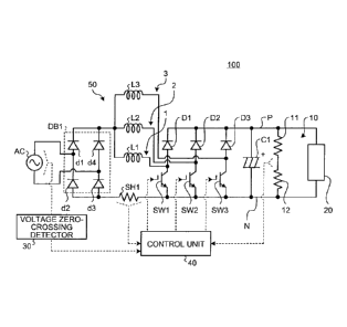
[0008] FIG. 1 is a configuration diagram of a converter
device according to a first embodiment of the present
invention.
FIG. 2 is a first chart for explaining an operation for
fault detection in the converter device according to the first
embodiment of the present invention.
FIG. 3 is a second chart for explaining an operation for
fault detection in the converter device according to the first
embodiment of the present invention.
FIG. 4 is a chart for explaining an advantage of
utilizing the supply voltage phase in fault detection
CA 3015049 2019-12-12
CA 03015049 2018-08-17
4
control in the converter device according to a second
embodiment of the present invention.
FIG. 5 is a chart for explaining a fault detection
operation utilizing the supply voltage phase in the
converter device according to the second embodiment of the
present invention.
FIG. 6 is a configuration diagram of the converter
device according to a third embodiment of the present
invention.
FIG. 7 is a diagram illustrating a bus current flowing
to a bus current detector during power factor regulation
control, and a target bus current.
FIG. 8 is a configuration diagram of the converter
device according to a fourth embodiment of the present
invention.
FIG. 9 is a diagram for explaining a fault detection
operation for a MOSFET in the converter device according to
the fourth embodiment of the present invention.
FIG. 10 is a configuration diagram of the converter
device according to a fifth embodiment of the present
invention.
Description of Embodiments
[0009] A converter device according to embodiments of
the present invention will be described below in detail
with reference to the drawings. Note that these
embodiments are not intended to limit this invention.
[0010] First Embodiment
FIG. 1 is a configuration diagram of a converter
device according to a first embodiment of the present
invention. A converter device 100 according to the first
embodiment includes an interleaved power factor regulation
circuit. The power factor regulation circuit is a circuit
I I
CA 03015049 2018-08-17
that includes multiple booster sections each including a
set of a reactor, a switching element, and a reverse-
blocking diode, and provides control to sequentially switch
the switching elements of the respective booster sections,
5 thereby enabling harmonic current to be reduced or
eliminated. Although FIG. 1 illustrates, by way of example,
a three-stage interleave circuit including three booster
sections 1, 2, and 3 coupled in parallel with one another,
the interleave circuit applied to the converter device 100
is not limited to a three-stage interleave circuit, but may
be an interleave circuit having two or more stages.
[0011] The converter device 100 illustrated in FIG. 1
includes a diode bridge DB1, which is a rectification
circuit that receives, as an input, AC power from a single-
phase AC power supply AC, and performs full-wave
rectification on the AC power received; a booster circuit
50 that boosts the output voltage from the diode bridge
DB1; a smoothing capacitor Cl that smooths the output
voltage from the booster circuit 50, and outputs the
smoothed voltage to a load 20; a bus voltage detection
circuit 10; a bus current detector SH1; a voltage zero-
crossing detector 30; and a control unit 40 that controls
the booster circuit 50. An example of the load 20 is an
air conditioner.
[0012] Although the diode bridge DB1 illustrated in FIG.
1 is a full-wave rectification circuit formed by a
combination of four diodes dl, d2, d3, and d4, the
configuration of the diode bridge DB1 is not limited
thereto, and the diode bridge DB1 may be configured by a
combination of metal oxide semiconductor field effect
transistors (MOSFETs).
[0013] The booster circuit 50 includes a booster section
1 including a reactor Li, a switching element SW1, and a
CA 03015049 2018-08-17
6
reverse-blocking diode Dl; a booster section 2 including a
reactor L2, a switching element SW2, and a reverse-blocking
diode D2; and a booster section 3 including a reactor L3, a
switching element SW3, and a reverse-blocking diode D3.
[0014] The AC power supply AC is connected to the diode
bridge DB1, and the positive end of the diode bridge DB1 is
connected to one end of the reactor Ll. The other end of
the reactor Li is connected to a connection terminal
between the switching element SW1 and the anode side of the
reverse-blocking diode Dl. The cathode side end of the
reverse-blocking diode D1 is connected to the positive end
of the smoothing capacitor Cl. The reactor Li, the
switching element SW1, and the reverse-blocking diode D1
connected as above configure the booster section 1.
[0015] The positive side of the diode bridge DB1 is also
connected to one end of the reactor L2. The other end of
the reactor L2 is connected to a connection terminal
between the switching element SW2 and the anode side of the
reverse-blocking diode D2. The cathode side end of the
reverse-blocking diode D2 is connected to the positive end
of the smoothing capacitor Cl. The reactor L2, the
switching element SW2, and the reverse-blocking diode D2
connected as above configure the booster section 2.
[0016] The positive side of the diode bridge DB1 is also
connected to one end of the reactor L3. The other end of
the reactor L3 is connected to a connection terminal
between the switching element SW3 and the anode side of the
reverse-blocking diode D3. The cathode side end of the
reverse-blocking diode D3 is connected to the positive end
of the smoothing capacitor Cl. The reactor L3, the
switching element SW3, and the reverse-blocking diode D3
connected as above configure the booster section 3.
[0017] The end portions of the three switching elements
6
CA 03015049 2018-08-17
7
SW1, SW2, and SW3 other than the end portions respectively
connected to the reactors Li, L2, and L3 are connected to
the negative end of the smoothing capacitor Cl and to one
end of the bus current detector SH1. The other end of the
bus current detector SH1 is connected to the negative end
of the diode bridge DB1.
[0018] The positive end of the smoothing capacitor Cl is
connected to a positive-side DC bus P, and the negative end
of the smoothing capacitor Cl is connected to a negative-
side DC bus N. Both ends of the smoothing capacitor Cl are
connected to the load 20.
[0019] The bus voltage detection circuit 10 includes a
voltage divider resistor 11 and a voltage divider resistor
12. One end of the serial circuit constituted by the
voltage divider resistor 11 and the voltage divider
resistor 12 is connected to the positive-side DC bus P, and
the other end of the serial circuit is connected to the
negative-side DC bus N. The combination of the voltage
divider resistors 11 and 12 divides and limits the charged
voltage the smoothing capacitor Cl within a voltage range
detectable by the control unit 40.
[0020] The voltage zero-crossing detector 30, which is a
phase detection section, detects the zero-crossing point of
the AC power from the AC power supply AC, and outputs
information on the zero-crossing point detected, to the
control unit 40. The bus current detector SH1 detects a
bus current flowing between the diode bridge DB1 and the
load 20, and outputs information on the bus current
detected, to the control unit 40.
[0021] The control unit 40 outputs a pulse width
modulation (PWM) signal for driving the switching elements
SW?, SW2, and SW3 based on pieces of the information output
from the voltage zero-crossing detector 30, from the bus
CA 03015049 2018-08-17
8
current detector SH1, and from the bus voltage detection
circuit 10 to provide ON and OFF control. This operation
provides power factor regulation control. Note that the
control unit 40 may receive information other than the
information described above, and the operation of the power
factor regulation control may use such other information.
[0022] The control unit 40 according to the present
embodiment performs fault detection on each of the booster
sections 1, 2, and 3 before the beginning of power factor
regulation control and when the load of the load 20 is very
low. It is assumed that before any of the switching
elements SW1, SW2, and SW3 is turned on, the load of the
load 20 is very low, and therefore, substantially no bus
current is flowing. In addition, a fault detection
operation on any one of the booster sections 1, 2, and 3
may hereinafter referred to simply as "fault detection."
[0023] An operation of fault detection in the control
unit 40 will next be described in detail referring to FIGS.
2 and 3.
[0024] FIG. 2 is a first chart for explaining an operation
for fault detection in the converter device according to the
first embodiment of the present invention. FIG. 2 illustrates
waveforms of the PWM signals for driving the corresponding
switching elements SW1, SW2, and SW3. In FIG. 2, the PWM
signals for providing ON and OFF control of the switching
elements SW1, SW2, and SW3 are respectively denoted by an
output to SW1, an output to SW2, and an output to SW3. FIG. 2
also illustrates a waveform of the bus current detected when
the output of PWM signal to SW1 is provided, a waveform of the
bus current detected when the output of PWM signal to SW2 is
provided, and a waveform of the bus current detected when the
output of PWM signal to SW3 is provided. FIG. 2 further
illustrates, using a dotted line, a fault determination
I 1
CA 03015049 2018-08-17
9
threshold for determining the presence or absence of a
fault in each of the booster sections 1, 2, and 3.
[0025] In the fault detection operation, the control
unit 40 first maintains the switching element SW1 in an ON
state for a certain time period. Turning on the switching
element SW1 establishes a current path including the AC
power supply AC, the diode bridge Dill, the reactor Li, the
switching element SW1, the bus current detector Sill, the
diode bridge DB1, and the AC power supply AC illustrated in
FIG. 1, thereby causing a bus current to start flowing.
[0026] Next, when the switching element SW1 is turned
off after the predetermined time period, the bus current
immediately before the turning off is detected by the bus
current detector SH1. The current detected at this time
point is the current that has flowed to the booster section
1 along the current path described above. Due to a high
inductance of the reactor Li in the current path, the
magnitude of the current generated by turning on the
switching element SW1 will not immediately decrease to zero
after the switching element SW1 is turned off. Thus, the
switching element SW1 is turned off and the off state is
maintained until the bus current attenuates to a very low
value. Then, the switching element SW2 is turned on, and
current detection is performed similarly to the case of the
switching element SW1 to detect the current that has flowed
to the booster section 2. Then, after a certain time
period is allowed to elapse to cause the bus current to
attenuate to a very low value, the switching element SW3 is
turned on to detect the current that has flowed to the
booster section 3, similarly.
[0027] When the magnitude of the bus current that has
flowed to one of the booster sections 1, 2, and 3 is
greater than or equal to the fault determination threshold,
CA 03015049 2018-08-17
it is determined that the one booster section is in a
normal condition. When all of the booster sections 1, 2,
and 3 are in a normal condition, it is determined that the
control unit 40 is in a normal condition.
5 [0028] FIG. 3 is a second chart for explaining an
operation for fault detection in the converter device
according to the first embodiment of the present invention.
FIG. 3 illustrates, similarly to FIG. 2, waveforms of the
outputs of PWM signal to SW1, SW2, and SW3, and a waveform
10 of the bus current detected when outputs of PWM signal to
SW1, SW2, and SW3 are provided. FIG. 3 differs from FIG. 2
in that an anomaly in the booster section 2 causes the
value of the bus current to be less than the threshold even
when the switching element SW2 is turned on. As described
above, having detected a bus current less than the
threshold level, the control unit 40 determines that the
booster section 2 has a fault.
[0029] Although FIGS. 2 and 3 illustrate the number of
switching operations for determining the presence or
absence of a fault as one for each of the booster sections
1, 2, and 3, such number may be two or more. That is, a
determination of the presence or absence of a fault may be
made by outputting a PWM signal multiple times to each of
the switching elements SW1, SW2, and SW3 to switch each of
the switching elements SW1, SW2, and SW3 multiple times.
When each of the switching elements SW1, SW2, and SW3 is
switched multiple times, the determination method may
follow, for example, a so-called majority rule to determine
that the device is in a normal condition when the value of
[the number of times the threshold is reached or
exceeded]/[the number of switching operations] is greater
than 1/2. Moreover, although FIGS. 2 and 3 illustrate that
the switching element SW1, switching element SW2, and the
CA 03015049 2018-08-17
11
switching element SW3 are sequentially switched in this
order, the switching elements SW!, SW2, and SW3 may be
switched in any order.
[0030] When the control unit 40 determines that all of
the booster sections 1, 2, and 3 are in a normal condition,
the control unit 40 then begins to perform power factor
regulation control, and permits the load of the load 20 to
increase. When at least one of the booster sections 1, 2,
and 3 is in an abnormal condition, the control unit 40
determines that the booster circuit 50 is in an abnormal
condition. Consequently, the control unit 40 does not
permit the power factor regulation control and an increase
in the load of the load 20. Alternatively, the control
unit 40 may be configured to, when one of the booster
sections 1, 2, and 3 has a fault, reduce the rated current
of the load 20 to 2/3, and permit an increase in the load
of the load 20 and the power factor regulation control
within that limit. The control unit 40 may further be
configured to, when two of the booster sections 1, 2, and
3 have a fault, permit an increase in the load of the load
20 and the power factor regulation control within 1/3 of
the rated current of the load 20, and permit the operation
to continue. The control unit 40 may further be
configured to, when all of the booster sections 1, 2, and
3 have a fault, recognize an abnormal condition, and
inhibit power factor regulation control and an increase in
the load of the load 20. Any of these operations can
prevent a current higher than a predicted level from
flowing to a circuit element, and can thus prevent an
overheat fault from occurring.
[0031] Second Embodiment
A second embodiment describes an example configuration
of the converter device 100 that uses a supply voltage
CA 03015049 2018-08-17
12
phase in the fault detection control. The converter device
100 of the second embodiment uses a circuit similar to the
configuration of the converter device 100 illustrated in
FIG. 1. The first embodiment and the second embodiment
differ from each other in the method of fault detection in
the control unit 40.
[0032] An advantage of the use of the supply voltage
phase in the fault detection control will first be
described. The magnitude of the current caused to flow by
turning on a switching element during a fault detection
operation depends on the amplitude of the supply voltage,
on the phase of the supply voltage at the time when that
switching element is turned on, on the inductance of the
corresponding reactor, and on the duration of the ON state
of that switching element. In this regard, the amplitude
of the supply voltage and the inductance of the
corresponding reactor are constant values, and the duration
of the ON state is also a predetermined value. However,
the phase of the supply voltage is undetermined in the
method of the first embodiment.
[0033] Here, FIG. 4 is a chart for explaining an
advantage of utilizing the supply voltage phase in the
fault detection control in the converter device according
to the second embodiment of the present invention. FIG. 4
illustrates the amplitude of the supply voltage, an output
to SW, and the bus current. As illustrated in FIG. 4, even
for the same amplitude of the supply voltage, the same
inductance of the corresponding reactor, and the same
duration of the ON state (hereinafter referred to as ON
duration), turning on a switching element when the supply
voltage phase is near 0 or 180 degrees results in a slow
increase in the bus current due to a low supply voltage,
and hence in a low current flow, while turning on a
CA 03015049 2018-08-17
13
switching element when the supply voltage phase is near 90
or 270 degrees results in a rapid increase in the current
due to a high supply voltage, and hence in a high current
flow. Thus, in the first embodiment, turning on a
switching element when the supply voltage phase is near 0
or 180 degrees needs a long ON duration to allow a bus
current significantly higher than the threshold to flow,
while turning on a switching element when the supply
voltage phase is near 90 or 270 degrees requires an
appropriately short ON duration to prevent breakdown of an
element due to a significantly high current. Accordingly,
determination of a suitable combination of the threshold
and the ON duration is not a straightforward matter. Thus,
when the supply voltage phase is detected and the supply
voltage phase at which a switching element is to be turned
on is specified, the magnitude of the bus current that will
flow can be previously predicted, thereby determination of
a suitable combination of the threshold and the ON duration
is facilitated.
[0034] FIG. 5 is a chart
for explaining a fault detection
operation utilizing the supply voltage phase in the converter
device according to the second embodiment of the present
invention. FIG. 5 illustrates the supply voltage, the supply
voltage phase, the outputs of PWM signal to SW1, SW2, and
SW3, and a wavefoLm of the bus current detected when the
outputs of PWM signal to SW1, SW2, and SW3 are provided.
The voltage zero-crossing detector 30 detects the time points
when the supply voltage phase is 0 degree and 360 degrees.
Thus, the control unit 40 operates to restart the timer in
the control unit 40 at the time point when the zero-crossing
signal output from the voltage zero-crossing detector 30
is received, and measures the input interval of the zero-
crossing signal using that timer. This operation enables
CA 03015049 2018-08-17
14
the control unit 40 to calculate the current supply voltage
phase (in degree) by [current count value of timer]/[timer
value for the interval of zero-crossing signa1]x360. In
the fault detection operation, the supply voltage phase is
determined using this technique; a switching element is
turned on at the time point when the supply voltage phase
reaches a certain value; and the magnitude of the current
is detected in the OFF state after a predetermined time
period elapses. The control unit 40 performs this
operation on each of the three booster sections 1, 2, and 3.
This operation is capable of eliminating the risk of
causing an excessively high current to flow during the
fault detection operation, and moreover, is capable of
eliminating the possibility that a current less than the
threshold level flows even in a normal phase, and thus a
fault becomes undetectable.
[0035] Note that, instead of the method in which the
supply voltage phase is determined and a switching element
is turned on at a particular supply voltage phase, another
method may be used in which the converter device 100
includes a supply voltage detector (not illustrated) that
detects an instantaneous value of the supply voltage, and
the control unit 40 turns on a switching element when the
instantaneous value of the supply voltage detected by the
supply voltage detector reaches a certain value. Such
configuration is also capable of providing an advantage
equivalent or similar to an advantage provided by the use
of the supply voltage phase.
[0036] Third Embodiment
FIG. 6 is a configuration diagram of the converter
device according to a third embodiment of the present
invention. The converter device 100 of the first
embodiment and a converter device 100-3 of the third
CA 03015049 2018-08-17
embodiment differ as below. The fault detection method is
similar to the fault detection method of the second
embodiment.
(1) In the interleaved power factor regulation circuit
5 of the third embodiment, bus current information for fault
detection and bus current information for power factor
improvement control that are analog signals detected by the
bus current detector SH1, are input to the control unit 40
through separate paths.
10 (2) The path for fault detection includes a filter
circuit, or a low-pass filter circuit having a small time
constant, which is inserted in the path for transmitting an
analog signal.
(3) The path for power factor regulation control
15 includes a low-pass filter circuit having a large time
constant that is inserted in the path for transmitting an
analog signal.
(4) The bus current information detected by the bus
current detector SH1 is subjected to a low-pass filtering
operation based on a first time constant, or alternatively
is not subjected to that low-pass filtering operation, for
detecting a fault of any of the booster sections 1, 2, and
3. The bus current information is subjected to a low-pass
filtering operation based on a second time constant that is
larger than the first time constant, for the power factor
regulation control.
[0037] A benefit of separating the bus current
information path will be described below. First, the bus
current flowing to the bus current detector SH1 during the
power factor regulation control will be described below
referring to FIG. 7. FIG. 7 is a diagram illustrating a
bus current flowing to the bus current detector during the
power factor regulation control, and a target bus current.
CA 03015049 2018-08-17
16
In FIG. 7, the dotted line indicates the waveform of the
target bus current, and this waveform is a sine curve. The
solid line indicates the waveform of the bus current that
actually flows to the bus current detector. The current is
made to have a waveform approximated to a sine curve by
repeatedly turning on and off the switching elements, and
therefore, the bus current consequently has a waveform
formed of a continuous set of triangular waves having an
ON/OFF frequency of that switching elements. The ON and
OFF frequency of the switching elements is referred to as
carrier frequency.
[0038] The carrier component of the bus current is
desirably removed before power factor regulation control.
To this end, a low-pass filter having a large time constant
is installed in the analog signal path for detecting the
current for the purpose of the power factor regulation
control.
[0039] In contrast, during the fault detection, a
switching element is turned off after the current has been
increased in a short time period, thereby making the
current waveform like a triangular wave. Accordingly, a
low-pass filter having a large time constant prevents the
current value from being accurately detected. Thus, for
the fault detection, a configuration is used such that a
low-pass filter having a very small time constant is
connected, or no filter is connected, in the analog signal
path.
[0040] The configuration of the third embodiment can
provide both fault detection and power factor regulation
control with high accuracy.
[0041] Note that when the bus current information, which
is an analog signal, is to be processed after being
converted into a digital signal in the control unit 40, the
CA 03015049 2018-08-17
17
low-pass filter may be implemented as a digital filter in
the control unit 40. In this case, control may be
performed without using the digital filter during the fault
detection, and control may be performed using digital
filter control during the power factor regulation control,
thereby control can be performed without need for
separating the path.
[0042] Fourth Embodiment
FIG. 8 is a configuration diagram of the converter
device according to a fourth embodiment of the present
invention. FIG. 8 illustrates an example configuration of
the booster circuit 50 in a case in which the interleaved
power factor regulation circuit utilizes synchronous
rectification. The converter device 100 of the first
embodiment and a converter device 100-4 of the fourth
embodiment differ as below.
(1) The converter device 100-4 of the fourth
embodiment includes a booster circuit 50A in place of the
booster circuit 50.
(2) The booster section 1 includes a transistor SR1,
which is a MOSFET, in place of the reverse-blocking diode
D1 of the first embodiment.
(3) The booster section 2 includes a transistor SR2,
which is a MOSFET, in place of the reverse-blocking diode
D2 of the first embodiment.
(4) The booster section 3 includes a transistor SR3,
which is a MOSFET, in place of the reverse-blocking diode
D3 of the first embodiment.
(5) The transistors SRI, SR2, and SR3 are each
controlled by a gate drive signal output from the control
unit 40. The transistor SR1 is maintained in the ON state
while the switching element SW1 is in the OFF state, and is
maintained in the OFF state while the switching element SW1
CA 03015049 2018-08-17
18
is in the ON state. The transistor 5R2 is maintained in
the ON state while the switching element SW2 is in the OFF
state, and is maintained in the OFF state while the
switching element SW2 is in the ON state. The transistor
SR3 is maintained in the ON state while the switching
element SW3 is in the OFF state, and is maintained in the
OFF state while the switching element SW3 is in the ON
state. This operation provides synchronous rectification,
thereby enabling electrical loss to be reduced.
[0043] The interleave circuit utilizing synchronous
rectification of the fourth embodiment can also detect a
fault of any of the switching element and the reactor in
each of the booster sections 1, 2, and 3 in accordance with
each control of the first, second, and third embodiments.
On the other hand, whether a MOSFET has a fault or not
needs to be determined by another method.
[0044] FIG. 9 is a diagram for explaining a fault
detection operation for a MOSFET in the converter device
according to the fourth embodiment of the present invention.
FIG. 9 illustrates the transistor SR1, the switching
element SW1, and the smoothing capacitor Cl, all of which
constitute a part of the circuit illustrated in FIG. 8. In
addition, the dotted line indicates the path of the current
flowing through the transistor SR1, the switching element
SW1, and the smoothing capacitor Cl.
[0045] For example, to detect a fault of the booster
section 1, the control unit 40 turns on both of the switching
element SW1 and the transistor SR1 and maintains the switching
element SW1 and the transistor SR1 in the ON state for a short
time period. This ON duration is set so as not to damage the
element due to an overcurrent. Under this condition, a
current flows along a path from the positive side of the
smoothing capacitor Cl through the transistor SR1 and the
CA 03015049 2018-08-17
19
switching element SW1 to the negative side of the smoothing
capacitor Cl to allow an electrical charge to be discharged
from the smoothing capacitor Cl, and thus bus voltage
across both ends of the smoothing capacitor Cl decreases.
[0046] The control unit 40 detects the bus voltage
before and after the switching element SW1 and the transistor
SR1 are both turned on, and determines that the transistor
SR1 is in a normal condition when the difference in the bus
voltage detected before and after the turning on is greater
than or equal to a threshold. Otherwise, when the difference
in the bus voltage detected before and after the turning on
is less than the threshold, the control unit 40 determines
that the path described above is not established, and thus,
that the transistor SR1 is in an abnormal condition.
[0047] Similarly to the detection of a fault of the
booster section 1, the control unit 40 turns on both of the
switching element SW2 and the transistor SR2 to detect a
fault of the transistor SR2, and turns on both of the
switching element SW3 and the transistor SR3 to detect a
fault of the transistor SR3. When a fault is detected, an
operation is performed similarly to the first embodiment.
Thus, the presence or absence of a fault of a MOSFET can be
detected.
[0048] Note that when only one turn-on operation does
not generate a sufficient voltage drop, thus making it hard
to make a determination due to a small difference in the
bus voltage between before and after both of the element SR
and the element SW are turned on, the control unit 40 may
perform the turn-on operation multiple times to cause a
further reduction in the voltage, and thus provide control
to increase the difference in the bus voltage.
[0049] Fifth Embodiment
FIG. 10 is a configuration diagram of the converter
CA 03015049 2018-08-17
device according to a fifth embodiment of the present
invention. Similarly to the fourth embodiment, a converter
device 100-5 of the fifth embodiment includes an interleave
circuit that utilizes synchronous rectification. The
5 converter device 100-4 of the fourth embodiment and the
converter device 100-5 of the fifth embodiment differ as
below.
(1) As illustrated in FIG. 10, the converter device
100-5 includes a current detector SH2 disposed between the
10 connection terminal of the switching elements SW1, SW2, and
SW3 and the negative-side DC bus N.
(2) The current detector SH2 detects the total amount
of the currents flowing through the switching elements SW1,
SW2, and SW3 respectively in the multiple booster sections
15 1, 2, and 3.
(3) The control unit 40 detects a fault of any of the
transistors SR1, SR2, and SR3 using the value of the
current detected by the current detector SH2.
[0050) For example, when, in the booster section 1, both
20 of the switching element SW1 and the transistor SR1 are
turned on, and the magnitude of the current detected by the
current detector SH2 is greater than or equal to a
threshold, the control unit 40 determines that the
transistor SR1 is in a normal condition, while when the
magnitude of the current detected by the current detector
SH2 is less than the threshold, the control unit 40
determines that the transistor SR1 is in an abnormal
condition. Determinations on the booster section 2 and on
the booster section 3 are performed similarly. Thus, the
presence or absence of faults of the transistors SR1, SR2,
and SR3 can be detected.
[0051] Note that, because the current detector SH2 is a
current detector merely for a protection function, the
CA 03015049 2018.--17
21
current detector SH2 may have an accuracy lower than the
accuracy of the bus current detector SH1, thereby enabling
the cost to be reduced.
[0052] In addition, the control unit 40 of the first
through fifth embodiments may be configured such that, upon
detection of a fault in at least one booster section of the
multiple booster sections 1, 2, and 3, the control unit 40
inhibits power factor regulation control and an increase of
the load of the load 20. This operation can prevent a
current higher than a predicted level from flowing to a
circuit element, and can thus prevent an overheat fault
from occurring.
[0053] Moreover, the control unit 40 of the first
through fifth embodiments may be configured to, when n
booster sections are detected as having a fault among
parallel-coupled m multiple booster sections 1, 2, ... m,
permit the power factor improvement operation, but limit
the increase of the load to (m-n)/m times the rated value
of the load. Here, m and n are each an integer greater
than or equal to 1, and satisfy n5.m. This operation can
prevent a current higher than a predicted level from
flowing to a circuit element, and can thus prevent an
overheat fault from occurring.
[0054] The configurations described in the foregoing
embodiments are merely examples of various aspects of the
present invention. These configurations may be combined
with a known other technology, and moreover, a part of such
configurations may be omitted and/or modified without
departing from the spirit of the present invention.
Reference Signs List
[0055] 1, 2, 3 booster section; 10 bus voltage
detection circuit; 11, 12 voltage divider resistor; 20
CA 03015049 2018-08-17
22
load; 30 voltage zero-crossing detector; 40 control unit;
50, 50A booster circuit; 100, 100-3, 100-4, 100-5
converter device; AC AC power supply; Cl smoothing
capacitor; D1, D2, D3 reverse-blocking diode; DB1 diode
bridge; dl, d2, d3, d4 diode; Li, L2, L3 reactor; N
negative-side DC bus; P positive-side DC bus; SH1 bus
current detector; SH2 current detector; SR1, SR2, SR3
transistor; SW1, SW2, SW3 switching element.