Note: Descriptions are shown in the official language in which they were submitted.
CA 03015622 2018-08-23
WO 2017/147382 PCT/US2017/019297
- 1 -
LOW CADMIUM CONTENT NANOSTRUCTURE COMPOSITIONS
AND USES THEREOF
BACKGROUND OF THE INVENTION
Field of the Invention
100011 The invention is in the field of nanotechnology. Low concentration
cadmium-
containing quantum dot compositions are disclosed which, when in a film within
a
display, exhibit high color gamut, high energy efficiency, and a narrow full
width at half
maximum at individual wavelength emissions.
Background Art
100021 Semiconductor nanostructures can be incorporated into a variety of
electronic and
optical devices. The electrical and optical properties of such nanostructures
vary, e.g.,
depending on their composition, shape, and size. For example, size-tunable
properties of
semiconductor nanoparticles are of great interest for applications such as
light emitting
diodes (LEDs), lasers, and biomedical labeling. Highly luminescent
nanostructures are
particularly desirable for such applications.
[0003] To exploit the full potential of nanostructures in applications such
as LEDs and
displays, the nanostructures need to simultaneously meet five criteria: narrow
and
symmetric emission spectra, high photoluminescence (PL) quantum yields (QYs),
high
optical stability, eco-friendly materials, and low-cost methods for mass
production. Most
previous studies on highly emissive and color-tunable quantum dots have
concentrated on
materials containing cadmium, mercury, or lead. Wang, A., et al., Nanoscale
7:2951-2959
(2015). But, there are increasing concerns that toxic materials such as
cadmium, mercury,
and lead pose serious threats to human health and the environment. The
European
Union's Restriction of Hazardous Substances rules ban any consumer electronics
containing more than trace amounts of these materials. Therefore, there is a
need to
produce materials that contain no more than trace amounts of cadmium, mercury,
and
lead for the production of LEDs and displays.
100041 Cadmium-free quantum dots based on indium phosphide are inherently
less stable
than the prototypic cadmium selenide quantum dots. The higher valence and
conduction
CA 03015622 2018-08-23
WO 2017/147382 PCT/US2017/019297
- 2 -
band energy levels make InP quantum dots more susceptible to photooxidation by
electron transfer from an excited quantum dot to oxygen, as well as more
susceptible to
photoluminescence quenching by electron-donating agents such as amines or
thiols which
can refill the hole states of excited quantum dots and thus suppress radiative
recombination of excitons. See, e.g., Chibli, H., et al., "Cytotoxicity of
InP/ZnS quantum
dots related to reactive oxygen species generation,"Nanoscak 3:2552-2559
(2011);
Blackburn, J.L., et al., "Electron and Hole Transfer from Indium Phosphide
Quantum
Dots,"J. Phys. Chem. B /09:2625-2631 (2005); and Selmarten, D., et al.,
"Quenching of
Semiconductor Quantum Dot Photoluminescence by a it-Conjugated Polymer," J.
Phys.
Chem. B 109:15927-15933 (2005).
100051 Inorganic shell coatings on quantum dots are a universal approach to
tailoring
their electronic structure. Additionally, deposition of an inorganic shell can
produce more
robust particles by passivation of surface defects. Ziegler, J., et al., Adv.
Mater. 20:4068-
4073 (2008). For example, shells of wider band gap semiconductor materials
such as ZnS
can be deposited on a core with a narrower band gap ¨ such as CdSe or InP ¨ to
afford
structures in which excitons are confined within the core. This approach
increases the
probability of radiative recombination and makes it possible to synthesize
very efficient
quantum dots with quantum yields close to unity and thin shell coatings.
100061 Core/shell quantum dots that have a shell of a wider band gap
semiconductor
material deposited onto a core with a narrower band gap are still prone to
degradation
mechanisms ¨ because a thin shell of less than a nanometer does not
sufficiently
suppress charge transfer to environmental agents. A thick shell coating of
several
nanometers would reduce the probability of tunneling or exciton transfer and
thus, it is
believed that a thick shell coating would improve stability ¨ a finding that
has been
demonstrated for the CdSe/CdS system.
100071 Regardless of the composition of quantum dots, most quantum dots do
not retain
their originally high quantum yield after continuous exposure to excitation
photons.
Elaborate shelling engineering such as the formation of multiple shells and
thick shells ¨
wherein the carrier wave functions in the core become distant from the surface
of the
quantum dot ¨ have been effective in mitigating the photoinduced quantum dot
deterioration. Furthermore, it has been found that the photodegradation of
quantum dots
CA 03015622 2018-08-23
WO 2017/147382 PCT/US2017/019297
- 3 -
can be retarded by encasing them with an oxide ¨ physically isolating the
quantum dot
surface from their environment. Jo, J.-H., et al., J. Alloys Compd. 647:6-13
(2015).
[0008] Thick coatings on CdSe/CdS giant shell quantum dots have been found
to improve
their stability towards environmental agents and surface charges by decoupling
the light-
emitting core from the surface over several nanometers. But, it is difficult
to retain the
beneficial properties of thin shell quantum dots when producing thick shells
due to the
manifold opportunities for failure and degradation such as: (1) dot
precipitation due to
increased mass, reduced surface-to-volume ratio, and increased total surface
area; (2)
irreversible aggregation with shell material bridging dots; (3) secondary
nucleation of
shell material; (4) relaxation of lattice strain resulting in interface
defects; (5) anisotropic
shell growth on preferred facets; (6) amorphous shell or non-epitaxial
interface; and (7) a
broadening of size distribution resulting in a broad emission peak.
[0009] The interfaces in these heterogeneous nanostructures need to be free
of defects
because defects act as trap sites for charge carriers and result in a
deterioration of both
luminescence efficiency and stability. Due to the naturally different lattice
spacings of
these semiconductor materials, the crystal lattices at the interface will be
strained. The
energy burden of this strain is compensated by the favorable epitaxial
alignment of thin
layers, but for thicker layers the shell material relaxes to its natural
lattice ¨ creating
misalignment and defects at the interface. There is an inherent tradeoff
between adding
more shell material and maintaining the quality of the material.
[0010] Recent advances have made it possible to obtain highly luminescent
plain core
nanocrystals. But, the synthesis of these plain core nanocrystals has shown
stability and
processibility problems and it is likely that these problems may be intrinsic
to plain core
nanocrystals. Thus, core/shell nanocrystals are preferred when the
nanocrystals must
undergo complicated chemical treatments ¨ such as for biomedical applications
¨ or
when the nanocrystals require constant excitation as with LEDs and lasers. See
Li, J.J., et
al., J. Am. Chem. Soc. 125:12567-12575 (2003).
[0011] There are two critical issues that must be considered to control the
size
distribution during the growth of shell materials: (1) the elimination of the
homogenous
nucleation of the shell materials; and (2) homogenous monolayer growth of
shell
precursors to all core nanocrystals in solution to yield shells with equal
thickness around
each core nanocrystal. Successive ion layer adsorption and reaction (S1LAR)
was
CA 03015622 2018-08-23
WO 2017/147382 PCT/US2017/019297
- 4 -
originally developed for the deposition of thin films on solid substrates from
solution
baths and has been introduced as a technique for the growth of high-quality
core/shell
nanocrystals of compound semiconductors.
100121 CdSe/CdS core/shell nanocrystals have been prepared with
photoluminescence
quantum yields of 20-40% using the SILAR method. Li, J.J., et al., J. Am.
Chem. Soc.
125:12567-12575 (2003). In the SILAR process, the amount of the precursors
used for
each half-reaction are calculated to match one monolayer coverage for all
cores ¨ a
technique that requires precise knowledge regarding the surface area for all
cores present
in the reaction mixture. And, the SILAR process assumes quantitative reaction
yields for
both half-reactions and thus, inaccuracies in measurements accumulate after
each cycle
and lead to a lack of control.
100131 The colloidal atomic layer deposition (c-ALD) process was proposed
in Ithurria,
S., et al., J. Am. Chem. Soc. 134:18585-18590 (2012) for the synthesis of
colloidal
nanostructures. In the c-ALD process, either nanoparticles or molecular
precursors are
sequentially transferred between polar and nonpolar phases to prevent
unreacted
precursors and byproducts from accumulating in the reaction mixture. The c-ALD
process
has been used to grow CdS layers on colloidal CdSe nanocrystals, CdSe
nanoplatelets,
and CdS nanorods. But, the c-ALD process suffers from the need to use phase
transfer
protocols that introduce exposure to potentially detrimental highly polar
solvents such as
formamide and N-methyl-formamide hydrazine.
100141 A need exists for quantum dot compositions with low levels of Cd and
high color
gamut. The present invention provides such compositions that are useful in
films, e.g. for
display devices.
BRIEF SUMMARY OF THE INVENTION
100151 The invention provides an optical film useful in a display device
comprising at
least one first population of cadmium-containing core-shell nanostructures and
at least
one second population of core-shell nanostructures that are not cadmium-
containing core-
shell nanostructures in a common matrix material. In one embodiment, the
optical film is
substantially free of cadmium. In another embodiment, the optical film
contains 10 to 99
ppm of cadmium. In another embodiment, the at least one second population of
nanostructures has a core selected from the group consisting of ZnO, ZnSe,
ZnS, ZnTe,
CA 03015622 2018-08-23
WO 2017/147382 PCT/US2017/019297
- 5 -
Hg0, HgSe, HgS, HgTe, BN, BP, BAs, AIN, AIP, AlAs, AlSb, GaN, GaP, GaAs, GaSb,
InN, InP, InAs, InSb, perovskite, and CuInxGai,SySe2_y. In another embodiment,
the shell
for each population is selected from the group consisting of Group BI-V
elements and
oxides thereof. In another embodiment, the shell for each population is
independently
selected from the group consisting of ZnS, ZnSe, ZnSSe, ZnTe, ZnTeS, and
ZnTeSe. In
another embodiment, the first population of core-shell nanostructures are
CdSe/ZnSe/ZnS
and the at least one second population of shellkore-nanostructures are
InP/ZnSe/ZnS. In
one embodiment, the emission spectra of each core-shell nanostructure has a
FWHM of
10-50 nm. In another embodiment, the optical film, when in a display device,
is capable
of achieving a Rec.2020 coverage of about 72% to about 98%. In another
embodiment,
the display device is capable of achieving a Rec.2020 coverage of greater than
about
90%. In another embodiment, the optical film comprises a green-emitting first
population
of cadmium-containing core-shell nanostructures with an emission maximum at
about
520-530 nm, a FWHM of less than 40 nm. In one embodiment, the FWHM is 20-40
nm.
In another embodiment, the FWHM is less than or equal to 30 nm. In another
embodiment, the quantum yield is about 85%-about 98%. In another embodiment,
the
quantum yield is greater than about 85%, greater than about 90%, greater than
about 95%,
or about 98%. In another embodiment, the optical film comprises a red-emitting
second
population of indium core-shell nanostructures with an emission maximum at
about 630
nm, a FWHM of about 20-45 urn, and a quantum yield of greater than about 70%,
e.g.,
greater than about 75%, e.g., about 78%.
100161 The invention also provides a display device, comprising the optical
film
described herein. In one embodiment, the display has a Rec.2020 coverage of
about 80%
to about 98%. In one embodiment, the Rec.2020 coverage is about 90%-about 98%.
100171 In another embodiment, the display device comprises:
a layer that emits radiation;
the optical film layer disposed on the radiation emitting layer;
an optically transparent barrier layer on the film layer; and
an optical element, disposed on the barrier layer.
100181 In one embodiment, the radiation emitting layer, the film layer, and
the optical
element are part of a pixel unit of the display device. In another embodiment,
the optical
element is a color filter. In another embodiment, the barrier layer comprises
an oxide. In
CA 03015622 2018-08-23
WO 2017/147382 PCT/US2017/019297
- 6 -
another embodiment, the film layer further comprises surfactants or ligands
bonded to the
optically transparent barrier layer. In another embodiment, the optically
transparent
barrier layer is configured to protect the nanostructures from degradation by
light flux,
heat, oxygen, moisture, or a combination thereof.
100191 In another embodiment, the invention provides an optical film for
use in a display
device having less than 100 ppm of cadmium and comprising at least one
population of
cadmium-containing core-shell quantum dots in a matrix material having a FWHM
less
than about 40 nm and a quantum efficiency greater than 90%, and the device
comprising
the optical film capable of achieving a Rec.2020 coverage of at least 85%. In
another
embodiment, the film further comprises at least one second population of non-
cadmium
containing core-shell quantum dots in the matrix material. In another
embodiment, the at
least second population of core-shell quantum dots comprises an InP core. In
another
embodiment, the display device comprising the optical film is capable of
achieving a
Rec.2020 coverage of greater than about 90%. In another embodiment, the first
population of core-shell quantum dots have a FWHM of less than about 30 nm. In
another
embodiment, the second population of core-shell quantum dots have a FWHM of
less
than about 45 nm. In another embodiment, the second population of core-shell
quantum
dots have a quantum efficiency of greater than about 75%. In another
embodiment, the
first population of core-shell quantum dots are CdSe/ZnSe/ZnS and the at least
one
second population of core-shell quantum dots is InP/ZnSe/ZnS.
BRIEF DESCRIPTION OF THE DRAWINGS
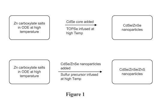
100201 FIGURE 1 depicts a scheme for a process of preparing a thick shell
coating on
CdSe nanostructures.
[0021] FIGURE 2 illustrates the concept of "gamut coverage" using the
Rec.2020 color
gamut in 1976 CIE(u',v') color space.
DETAILED DESCRIPTION OF THE INVENTION
Definitions
100221 Unless defined otherwise, all technical and scientific terms used
herein have the
same meaning as commonly understood by one of ordinary skill in the art to
which the
CA 03015622 2018-08-23
WO 2017/147382 PCT/US2017/019297
- 7 -
invention pertains. The following definitions supplement those in the art and
are directed
to the current application and are not to be imputed to any related or
unrelated case, e.g.,
to any commonly owned patent or application. Although any methods and
materials
similar or equivalent to those described herein can be used in the practice
for testing of
the present invention, the preferred materials and methods are described
herein.
Accordingly, the terminology used herein is for the purpose of describing
particular
embodiments only, and is not intended to be limiting.
100231 As used in this specification and the appended claims, the singular
forms "a," "an"
and "the" include plural referents unless the context clearly dictates
otherwise. Thus, for
example, reference to "a nanostructure" includes a plurality of such
nanostructures, and
the like.
100241 The term "about" as used herein indicates the value of a given
quantity varies by
10% of the value. For example, "about 100 nm" encompasses a range of sizes
from 90 nm
to 110 nm, inclusive.
100251 A "nanostructure" is a structure having at least one region or
characteristic
dimension with a dimension of less than about 500 nm. In some embodiments, the
nanostructure has a dimension of less than about 200 nm, less than about 100
nm, less
than about 50 nm, less than about 20 nm, or less than about 10 nm. Typically,
the region
or characteristic dimension will be along the smallest axis of the structure.
Examples of
such structures include nanowires, nanorods, nanotubes, branched
nanostructures,
nanotetrapods, tripods, bipods, nanocrystals, nanodots, quantum dots,
nanoparticles, and
the like. Nanostructures can be, e.g., substantially crystalline,
substantially
monocrystalline, polycrystalline, amorphous, or a combination thereof In some
embodiments, each of the three dimensions of the nanostructure has a dimension
of less
than about 500 nm, less than about 200 nm, less than about 100 nm, less than
about 50
nm, less than about 20 nm, or less than about 10 nm.
100261 The term "heterostructure" when used with reference to
nanostructures refers to
nanostructures characterized by at least two different and/or distinguishable
material
types. Typically, one region of the nanostructure comprises a first material
type, while a
second region of the nanostructure comprises a second material type. In
certain
embodiments, the nanostructure comprises a core of a first material and at
least one shell
of a second (or third etc.) material, where the different material types are
distributed
CA 03015622 2018-08-23
WO 2017/147382 PCT/US2017/019297
- 8 -
radially about the long axis of a nanowire, a long axis of an arm of a
branched nanowire,
or the center of a nanocrystal, for example. A shell can but need not
completely cover the
adjacent materials to be considered a shell or for the nanostructure to be
considered a
heterostructure; for example, a nanocrystal characterized by a core of one
material
covered with small islands of a second material is a heterostructure. In other
embodiments, the different material types are distributed at different
locations within the
nanostructure; e.g., along the major (long) axis of a nanowire or along a long
axis of arm
of a branched nanowire. Different regions within a heterostructure can
comprise entirely
different materials, or the different regions can comprise a base material
(e.g., silicon)
having different dopants or different concentrations of the same dopant.
100271 As used herein, the "diameter" of a nanostructure refers to the
diameter of a cross-
section normal to a first axis of the nanostructure, where the first axis has
the greatest
difference in length with respect to the second and third axes (the second and
third axes
are the two axes whose lengths most nearly equal each other). The first axis
is not
necessarily the longest axis of the nanostructure; e.g., for a disk-shaped
nanostructure, the
cross-section would be a substantially circular cross-section normal to the
short
longitudinal axis of the disk. Where the cross-section is not circular, the
diameter is the
average of the major and minor axes of that cross-section. For an elongated or
high aspect
ratio nanostructure, such as a nanowire, the diameter is measured across a
cross-section
perpendicular to the longest axis of the nanowire. For a spherical
nanostructure, the
diameter is measured from one side to the other through the center of the
sphere.
100281 The terms "crystalline" or "substantially crystalline," when used
with respect to
nanostmctures, refer to the fact that the nanostructures typically exhibit
long-range
ordering across one or more dimensions of the structure. It will be understood
by one of
skill in the art that the term "long range ordering" will depend on the
absolute size of the
specific nanostmctures, as ordering for a single crystal cannot extend beyond
the
boundaries of the crystal. In this case, "long-range ordering" will mean
substantial order
across at least the majority of the dimension of the nanostructure. In some
instances, a
nanostructure can bear an oxide or other coating, or can be comprised of a
core and at
least one shell. In such instances it will be appreciated that the oxide,
shell(s), or other
coating can but need not exhibit such ordering (e.g. it can be amorphous,
polycrystalline,
or otherwise). In such instances, the phrase "crystalline," "substantially
crystalline,"
CA 03015622 2018-08-23
WO 2017/147382 PCT/US2017/019297
- 9 -
"substantially monocrystalline," or "monocrystalline" refers to the central
core of the
nanostructure (excluding the coating layers or shells). The terms
"crystalline" or
"substantially crystalline" as used herein are intended to also encompass
structures
comprising various defects, stacking faults, atomic substitutions, and the
like, as long as
the structure exhibits substantial long range ordering (e.g., order over at
least about 80%
of the length of at least one axis of the nanostructure or its core). In
addition, it will be
appreciated that the interface between a core and the outside of a
nanostructure or
between a core and an adjacent shell or between a shell and a second adjacent
shell may
contain non-crystalline regions and may even be amorphous. This does not
prevent the
nanostructure from being crystalline or substantially crystalline as defined
herein.
100291 The term "monocrystalline" when used with respect to a nanostructure
indicates
that the nanostructure is substantially crystalline and comprises
substantially a single
crystal. When used with respect to a nanostructure heterostructure comprising
a core and
one or more shells, "monocrystalline" indicates that the core is substantially
crystalline
and comprises substantially a single crystal.
[0030] A "nanocrystal" is a nanostructure that is substantially
monocrystalline. A
nanocrystal thus has at least one region or characteristic dimension with a
dimension of
less than about 500 nm. In some embodiments, the nanocrystal has a dimension
of less
than about 200 nm, less than about 100 nm, less than about 50 nm, less than
about 20 nm,
or less than about 10 nm. The term "nanocrystal" is intended to encompass
substantially
monocrystalline nanostructures comprising various defects, stacking faults,
atomic
substitutions, and the like, as well as substantially monocrystalline
nanostructures without
such defects, faults, or substitutions. In the case of nanocrystal
heterostructures
comprising a core and one or more shells, the core of the nanocrystal is
typically
substantially monocrystalline, but the shell(s) need not be. In some
embodiments, each of
the three dimensions of the nanocrystal has a dimension of less than about 500
nm. In
other embodiments, each of the dimensions of the nanocrystal has a dimension
of less
than about 200 nm, less than about 100 nm, less than about 50 nm, less than
about 20 nm,
or less than about 10 nm.
[0031] The term "quantum dot" (or "dot") refers to a nanocrystal that
exhibits quantum
confinement or exciton confinement. Quantum dots can be substantially
homogenous in
material properties, or in certain embodiments, can be heterogeneous, e.g.,
including a
CA 03015622 2018-08-23
WO 2017/147382 PCT/US2017/019297
- 10 -
core and at least one shell. The optical properties of quantum dots can be
influenced by
their particle size, chemical composition, and/or surface composition, and can
be
determined by suitable optical testing available in the art. The ability to
tailor the
nanocrystal size, e.g., in the range between about 1 nm and about 15 mn,
enables
photoemission coverage in the entire optical spectrum to offer great
versatility in color
rendering.
100321 As used herein, "RoHS compliant" optical films refers to optical
films with less
than 1000 ppm of lead (Pb), less than 100 ppm cadmium (Cd), less than 100 ppm
mercury
(Fig), less than 1000 ppm hexavalent chromium (Hex-Cr), less than 1000 ppm
polybrominated biphenyls (PBB), and less than 1000 ppm polybrominated diphenyl
ethers (PBDE). The Restriction of Hazardous substances (RoHS) directive aims
to restrict
certain dangerous substances commonly used in electrical and electronic
equipment.
RoHS compliant components are tested for the presence of cadmium and
hexavalent
chromium, there must be less than 0.01% of the substance by weight at the raw
homogeneous materials level. For lead, PBB, and PBDE, there must be no more
than
0.1% of the material, when calculated by weight at raw homogeneous materials.
Any
RoHS compliant component must have 100 ppm or less of mercury and the mercury
must
not have been intentionally added to the component. In the EU, some military
and
medical equipment are exempt from RoHS compliance.
100331 A "ligand" is a molecule capable of interacting (whether weakly or
strongly) with
one or more faces of a nanostructure, e.g., through covalent, ionic, van der
Waals, or
other molecular interactions with the surface of the nanostructure.
100341 "Photoluminescence quantum yield" is the ratio of photons emitted to
photons
absorbed, e.g., by a nanostructure or population of nanostructures. As known
in the art,
quantum yield is typically determined by a comparative method using well-
characterized
standard samples with known quantum yield values.
100351 As used herein, the term "shell" refers to material deposited onto
the core or onto
previously deposited shells of the same or different composition and that
result from a
single act of deposition of the shell material. The exact shell thickness
depends on the
material as well as the precursor input and conversion and can be reported in
nanometers
or monolayers. As used herein, "target shell thickness" refers to the intended
shell
thickness used for calculation of the required precursor amount. As used
herein, "actual
CA 03015622 2018-08-23
WO 2017/147382 PCT/US2017/019297
- 11 -
shell thickness" refers to the actually deposited amount of shell material
after the
synthesis and can be measured by methods known in the art. By way of example,
actual
shell thickness can be measured by comparing particle diameters determined
from TEM
images of nanocrystals before and after a shell synthesis.
100361 As used herein, the term "full width at half-maximum" (FWHM) is a
measure of
the size distribution of quantum dots. The emission spectra of quantum dots
generally
have the shape of a Gaussian curve. The width of the Gaussian curve is defined
as the
FWHM and gives an idea of the size distribution of the particles. A smaller
FWHM
corresponds to a narrower quantum dot nanocrystal size distribution. FWHM is
also
dependent upon the emission wavelength maximum.
100371 "Alkyl" as used herein refers to a straight or branched, saturated,
aliphatic radical
having the number of carbon atoms indicated. In some embodiments, the alkyl is
C1_2
alkyl, Ci.3 alkyl, C1.4 alkyl, C1..5 alkyl, C1.6 alkyl, Ci.7 alkyl, C1..5
alkyl, C1.9 alkyl, C1.10
alkyl, C1-12 alkyl, C1..14 alkyl, C1-16 alkyl, C1-18 alkyl, C1-20 alkyl, C8-20
alkyl, C12-20 alkyl,
C14-20 alkyl, C16-20 alkyl, or C18-20 alkyl. For example, C1_6 alkyl includes,
but is not
limited to, methyl, ethyl, propyl, isopropyl, butyl, isobutyl, sec-butyl, tert-
butyl, pentyl,
isopentyl, and hexyl. In some embodiments, the alkyl is octyl, nonyl, decyl,
undecyl,
dodecyl, tridecyl, tetradecyl, pentadecyl, hexadecyl, heptadecyl, octadecyl,
nonadecyl, or
icosanyl.
100381 Unless clearly indicated otherwise, ranges listed herein are
inclusive.
100391 A variety of additional terms are defined or otherwise characterized
herein.
Production of a Core
[0040] Methods for colloidal synthesis of a variety of nanostructures are
known in the art.
Such methods include techniques for controlling nanostructure growth, e.g., to
control the
size and/or shape distribution of the resulting nanostructures.
[0041] In a typical colloidal synthesis, semiconductor nanostructures are
produced by
rapidly injecting precursors that undergo pyrolysis into a hot solution (e.g.,
hot solvent
and/or surfactant). The precursors can be injected simultaneously or
sequentially. The
precursors rapidly react to form nuclei. Nanostructure growth occurs through
monomer
addition to the nuclei, typically at a growth temperature that is lower than
the
injection/nucleation temperature.
CA 03015622 2018-08-23
WO 2017/147382 PCT/US2017/019297
-12-
100421 Ligands interact with the surface of the nanostructure. At the
growth temperature,
the ligands rapidly adsorb and desorb from the nanostructure surface,
permitting the
addition and/or removal of atoms from the nanostructure while suppressing
aggregation
of the growing nanostructures. In general, a ligand that coordinates weakly to
the
nanostructure surface permits rapid growth of the nanostructure, while a
ligand that binds
more strongly to the nanostructure surface results in slower nanostructure
growth. The
ligand can also interact with one (or more) of the precursors to slow
nanostructure
growth.
[0043] Nanostructure growth in the presence of a single ligand typically
results in
spherical nanostructures. Using a mixture of two or more ligands, however,
permits
growth to be controlled such that non-spherical nanostructures can be
produced, if, for
example, the two (or more) ligands adsorb differently to different
crystallographic faces
of the growing nanostructure.
[0044] A number of parameters are thus known to affect nanostructure growth
and can be
manipulated, independently or in combination, to control the size and/or shape
distribution of the resulting nanostructures. These include, e.g., temperature
(nucleation
and/or growth), precursor composition, time-dependent precursor concentration,
ratio of
the precursors to each other, surfactant composition, number of surfactants,
and ratio of
suifactant(s) to each other and/or to the precursors.
[0045] The synthesis of Group III-VI nanostructures has been described in
U.S. Patent
Nos. 6,225,198, 6,322,901, 6,207,229, 6,607,829, 7,060,243, 7,374,824,
6,861,155,
7,125,605, 7,566,476, 8,158,193, and 8,101,234 and in U.S. Patent Appl.
Publication Nos.
2011/0262752 and 2011/0263062. The synthesis of Group II-V nanostructures has
been
described in U.S. Patent Nos. 5,505,928, 6,306,736, 6,576,291, 6,788,453,
6,821,337, and
7,138,098, 7,557,028, 8,062,967, 7,645,397, and 8,282,412 and in U.S. Patent
Appl.
Publication No. 2015/236195.
100461 The synthesis of Group II-V nanostructures has also been described
in Wells,
R.L., et al., "The use of tris(trimethylsilyl)arsine to prepare gallium
arsenide and indium
arsenide," C'hem. Mater. /:4-6 (1989) and in Guzelian, A.A., et al.,
"Colloidal chemical
synthesis and characterization of InAs nanocrystal quantum dots," App!. Phys.
Lett. 69:
1432-1434(1996).
CA 03015622 2018-08-23
WO 2017/147382 PCT/US2017/019297
- 13 -
[0047] Synthesis of InP-based nanostnictures has been described, e.g., in
Xie, R., et al.,
"Colloidal InP nanocrystals as efficient emitters covering blue to near-
infrared," J. Am.
Chem. Soc. 129:15432-15433 (2007); Micic, 0.I., et al., "Core-shell quantum
dots of
lattice-matched ZnCdSe2 shells on InP cores: Experiment and theory," j Phys.
Chem. B
104:12149-12156(2000); Liu, Z., et al., "Coreduction colloidal synthesis of II-
V
nanocrystals: The case of InP,"Angew. Chem. Int. Ed. EngL 47:3540-3542 (2008);
Li, L.
et al., "Economic synthesis of high quality InP nanocrystals using calcium
phosphide as
the phosphorus precursor," Chem. Mater. 20:2621-2623 (2008); D. Battaglia and
X.
Peng, "Formation of high quality InP and InAs nanocrystals in a
noncoordinating
solvent," Nano Letters 2:1027-1030 (2002); Kim, S., et al., "Highly
luminescent
InP/GaP/ZnS nanocrystals and their application to white light-emitting
diodes," J. Am.
Chem. Soc. /34:3804-3809 (2012); Nann, T., et al., "Water splitting by visible
light: A
nanophotocathode for hydrogen production," Angew. Chem. Int. Ed 49:1574-1577
(2010); Borchert, H., et al., "Investigation of ZnS passivated InP
nanocrystals by XPS,"
Nano Letters 2:151-154 (2002); L. Li and P. Reiss, "One-pot synthesis of
highly
luminescent InP/ZnS nanocrystals without precursor injection," J. Am. Chem.
Soc.
130:11588-11589 (2008); Hussain, S., et al. "One-pot fabrication of high-
quality InP/ZnS
(core/shell) quantum dots and their application to cellular imaging,"
Chemphyschem.
10:1466-1470 (2009); Xu, S., et al., "Rapid synthesis of high-quality InP
nanocrystals," J.
Am. Chem. Soc. 128:1054-1055 (2006); Miele, 0.I., et al., "Size-dependent
spectroscopy
of InP quantum dots," J. Phys. Chem. B /01:4904-4912 (1997); Haubold, S., et
al.,
"Strongly luminescent InP/ZnS core-shell nanoparticles," Chemphyschem. 5:331-
334
(2001); CrosGagneux, A., et al., "Surface chemistry of InP quantum dots: A
comprehensive study," J. Am. Chem. Soc. 132:18147-18157 (2010); Micic, 0.I.,
et al.,
"Synthesis and characterization of InP, GaP, and GalnP2 quantum dots," J.
Phys. Chem.
99:7754-7759 (1995); Guzelian, A.A., et al., "Synthesis of size-selected,
surface-
passivated IriP nanocrystals,"./ Phys. Chem. /00:7212-7219(1996); Lucey, D.W.,
et al.,
"Monodispersed InP quantum dots prepared by colloidal chemistry in a non-
coordinating
solvent," Chem. Mater. /7:3754-3762 (2005); Lim, J., et al., "InP@ZnSeS,
core@composition gradient shell quantum dots with enhanced stability," Chem.
Mater.
23:4459-4463 (2011); and Zan, F., et al., "Experimental studies on blinking
behavior of
CA 03015622 2018-08-23
WO 2017/147382 PCT/US2017/019297
- 14 -
single InP/ZnS quantum dots: Effects of synthetic conditions and UV
irradiation," J.
Phys. Chem. C116:394-3950 (2012).
100481 In some embodiments, the core is a Group II-VI nanocrystal selected
from the
group consisting of ZnO, ZnSe, ZnS, ZnTe, CdO, CdSe, CdS, CdTe, Hg0, HgSe,
HgS,
HgTe, perovskite, and CuInõGai,SySe2_y. In some embodiments, the core is a
nanocrystal
selected from the group consisting of ZnSe, ZnS, CdSe, and CdS.
100491 In some embodiments, the at least one first core is a cadmium-
containing
nanostnicture and an at least one second core is a Group II-VI nanostructure.
In some
embodiments, the second core is a Group II-VI nanocrystal selected from the
group
consisting of BN, BP, BAs, AIN, AIP, AlAs, AlSb, GaN, GaP, GaAs, GaSb, InN,
InP,
InAs, InSb, perovskite, and CuInõGal,SySe2_y. In some embodiments, the at
least one
second core is a InP nanocrystal.
[0050] In some embodiments, the core is doped. In some embodiments, the
dopant of the
nanocrystal core comprises a metal, including one or more transition metals.
In some
embodiments, the dopant is a transition metal selected from the group
consisting of Ti,
Zr, Hf, V, Nb, Ta, Cr, Mo, W, Mn, Tc, Re, Fe, Ru, Os, Co, Rh, Tr, Ni, Pd, Pt,
Cu, Ag, Au,
and combinations thereof. In some embodiments, the dopant comprises a non-
metal. In
some embodiments, the dopant is ZnS, ZnSe, ZnTe, CdSe, CdS, CdTe, HgS, HgSe,
HgTe, CuInS2, CuInSei, AIN, AlP, AlAs, GaN, GaP, or GaAs.
[0051] In some embodiments, the core is purified before deposition of a
shell. In some
embodiments, the core is filtered to remove precipitate from the core
solution.
[0052] In some embodiments, the core is subjected to an acid etching step
before
deposition of a shell.
[0053] In some embodiments, the diameter of the core is determined using
quantum
confinement. Quantum confinement in zero-dimensional nanocrystallites, such as
quantum dots, arises from the spatial confinement of electrons within the
crystallite
boundary. Quantum confinement can be observed once the diameter of the
material is of
the same magnitude as the de Broglie wavelength of the wave function. The
electronic
and optical properties of nanoparticles deviate substantially from those of
bulk materials.
A particle behaves as if it were free when the confining dimension is large
compared to
the wavelength of the particle. During this state, the bandgap remains at its
original
energy due to a continuous energy state. However, as the confining dimension
decreases
CA 03015622 2018-08-23
WO 2017/147382 PCT/US2017/019297
- 15 -
and reaches a certain limit, typically in nanoscale, the energy spectrum
becomes discrete.
As a result, the bandgap becomes size-dependent.
Production of a Shell
100541 In some embodiments, the nanostructures include a core and at least
one shell. In
some embodiments, the nanostructures include a core and at least two shells.
The shell
can, e.g., increase the quantum yield and/or stability of the nanostructures.
In some
embodiments, the core and the shell comprise different materials. In some
embodiments,
the nanostructure comprises shells of different shell material.
100551 In some embodiments, shell material is deposited onto a core or a
core/shell(s)
that comprises a mixture of Group TT and VI materials. In some embodiments,
the shell
material comprises at least two of a zinc source, a selenium source, a sulfur
source, a
tellurium source, and a cadmium source. In some embodiments, the shell
material
comprise two of a zinc source, a selenium source, a sulfur source, a tellurium
source, and
a cadmium source. In some embodiments, the shell material comprises three of a
zinc
source, a selenitun source, a sulfur source, a tellurium source, and a cadmium
source. In
some embodiments, the shell material deposited is ZnS, ZnSe, ZnSSe, ZnTe,
ZnTeS, or
ZnTeSe. In other embodiments, alloyed shells containing low levels of cadmium
can also
be used.
100561 The thickness of the shell can be controlled by varying the amount
of precursor
provided. For a given shell thickness, at least one of the precursors is
optionally provided
in an amount whereby, when a growth reaction is substantially complete, a
shell of a
predetermined thickness is obtained. If more than one different precursor is
provided,
either the amount of each precursor can be limited or one of the precursors
can be
provided in a limiting amount while the others are provided in excess.
100571 The thickness of each shell can be determined using techniques known
to those of
skill in the art. In some embodiments, the thickness of each shell is
determined by
comparing the average diameter of the nanostructure before and after the
addition of each
shell. In some embodiments, the average diameter of the nanostructure before
and after
the addition of each shell is determined by transmission electron microscopy.
In some
embodiments, each shell has a thickness of between 0.05 nm and 3.5 run,
between 0.05
nm and 2 nm, between 0.05 nm and 1 nm, between 0.05 nm and 0.5 nm, between
0.05 nm
and 0.3 nm, between 0.05 nm and 0.1 nm, between 0.1 nm and 3.5 nm, between 0.1
nm
CA 03015622 2018-08-23
WO 2017/147382 PCT/US2017/019297
- 16 -
and 2 nm, between 0.1 nm and 1 nm, between 0.1 nm and 0.5 nm, between 0.1 nm
and
0.3 nm, between 0.3 nm and 3.5 nm, between 0.3 nm and 2 nm, between 0.3 nm and
1
nm, between 0.3 nm and 0.5 nm, between 0.5 nm and 3.5 nm, between 0.5 nm and 2
nm,
between 0.5 nm and 1 nm, between 1 nm and 3.5 nm, between 1 nm and 2 nm, or
between 2 nm and 3.5 nm.
100581 In some embodiments, each shell is synthesized in the presence of at
least one
nanostructure ligand. Ligands can, e.g., enhance the miscibility of
nanostructures in
solvents or polymers (allowing the nanostructures to be distributed throughout
a
composition such that the nanostructures do not aggregate together), increase
quantum
yield of nanostructures, and/or preserve nanostructure luminescence (e.g.,
when the
nanostructures are incorporated into a matrix). In some embodiments, the
ligand(s) for the
core synthesis and for the shell synthesis are the same. In some embodiments,
the
ligand(s) for the core synthesis and for the shell synthesis are different.
Following
synthesis, any ligand on the surface of the nanostructures can be exchanged
for a different
ligand with other desirable properties. Examples of ligands are disclosed in
U.S. Patent
Nos. 7,572,395, 8,143,703, 8,425,803, 8,563,133, 8,916,064, 9,005,480,
9,139,770, and
9,169,435, and in U.S. Patent Application Publication No. 2008/0118755.
100591 Ligands suitable for the synthesis of a shell are known by those of
skill in the art.
In some embodiments, the ligand is a fatty acid selected from the group
consisting of
lauric acid, caproic acid, myristic acid, palmitic acid, stearic acid, and
oleic acid. In some
embodiments, the ligand is an organic phosphine or an organic phosphine oxide
selected
from trioctylphosphine oxide (TOPO), trioctylphosphine (TOP),
diphenylphosphine
(DPP), triphenylphosphine oxide, and tributylphosphine oxide. In some
embodiments, the
ligand is an amine selected from the group consisting of dodecylamine,
oleylamine,
hexadecylamine, dioctylamine, and octadecylamine. In some embodiments, the
ligand is
tributylphosphine, oleic acid, or zinc oleate.
100601 In some embodiments, each shell is produced in the presence of a
mixture of
ligands. In some embodiments, each layer of a shell is produced in the
presence of a
mixture comprising 2, 3, 4, 5, or 6 different ligands. in some embodiments,
each shell is
produced in the presence of a mixture comprising 3 different ligands. In some
embodiments, the mixture of ligands comprises tributylphosphine, oleic acid,
and zinc
oleate.
CA 03015622 2018-08-23
WO 2017/147382 PCT/US2017/019297
-17-
100611 In some embodiments, each shell is produced in the presence of a
solvent. In some
embodiments, the solvent is selected from the group consisting of 1-
octadecene, 1-
hexadecene, 1-eicosene, eicosane, octadecane, hexadecane, tetradecane,
squalene,
squalane, trioctylphosphine oxide, and dioctyl ether. In some embodiments, the
solvent is
1-octadecene.
100621 In some embodiments, a core or a core/shell(s) and shell materials
are contacted at
an addition temperature between 20 C and 310 C, between 20 C and 280 C,
between
20 C and 250 C, between 20 C and 200 C, between 20 C and 150 C, between
20 C
and 100 C, between 20 C and 50 C, between 50 C and 310 C, between 50 C
and
280 C, between 50 C and 250 C, between 50 C and 200 C, between 50 C and
150
C, between 50 C and 100 C, between 100 C and 310 C, between 100 C and 280
C,
between 100 C and 250 C, between 100 C and 200 C, between 100 C and 150
C,
between 150 C and 310 C, between 150 C and 280 C, between 150 C and 250 C,
between 150 C and 200 C, between 200 C and 310 C, between 200 C and 280
C,
between 200 C and 250 C, between 250 C and 310 C, between 250 C and 280
C, or
between 280 C and 310 C. In some embodiments, a core or a core/shell(s) and
shell
materials are contacted at an addition temperature between 20 C and 100 C.
100631 In some embodiments, after contacting a core or core/shell(s) and
shell materials,
the temperature of the reaction mixture is increased to an elevated
temperature between
200 C and 310 C, between 200 C and 280 C, between 200 C and 250 C,
between
200 C and 220 C, between 220 C and 310 C, between 220 C and 280 C,
between
220 C and 250 C, between 250 C and 310 C, between 250 C and 280 C, or
between
280 C and 310 C. In some embodiments, after contacting a core or
core/shell(s) and
shell materials, the temperature of the reaction mixture is increased to
between 250 C
and 310 C.
100641 In some embodiments, after contacting a core or core/shell(s) and
shell materials,
the time for the temperature to reach the elevated temperature is between 2
and 240
minutes, between 2 and 200 minutes, between 2 and 100 minutes, between 2 and
60
minutes, between 2 and 40 minutes, between 5 and 240 minutes, between 5 and
200
minutes, between 5 and 100 minutes, between 5 and 60 minutes, between 5 and 40
minutes, between 10 and 240 minutes, between 10 and 200 minutes, between 10
and 100
minutes, between 10 and 60 minutes, between 10 and 40 minutes, between 40 and
240
CA 03015622 2018-08-23
WO 2017/147382 PCT/US2017/019297
- 18 -
minutes, between 40 and 200 minutes, between 40 and 100 minutes, between 40
and 60
minutes, between 60 and 240 minutes, between 60 and 200 minutes, between 60
and 100
minutes, between 100 and 240 minutes, between 100 and 200 minutes, or between
200
and 240 minutes.
[0065] In some embodiments, after contacting a core or core/shell(s) and
shell materials,
the temperature of the reaction mixture is maintained at an elevated
temperature for
between 2 and 240 minutes, between 2 and 200 minutes, between 2 and 100
minutes,
between 2 and 60 minutes, between 2 and 40 minutes, between 5 and 240 minutes,
between 5 and 200 minutes, between 5 and 100 minutes, between 5 and 60
minutes,
between 5 and 40 minutes, between 10 and 240 minutes, between 10 and 200
minutes,
between 10 and 100 minutes, between 10 and 60 minutes, between 10 and 40
minutes,
between 40 and 240 minutes, between 40 and 200 minutes, between 40 and 100
minutes,
between 40 and 60 minutes, between 60 and 240 minutes, between 60 and 200
minutes,
between 60 and 100 minutes, between 100 and 240 minutes, between 100 and 200
minutes, or between 200 and 240 minutes. In some embodiments, after contacting
a core
or core/shell(s) and shell materials, the temperature of the reaction mixture
is maintained
at an elevated temperature for between 30 and 120 minutes.
100661 In some embodiments, additional shells are produced by further
additions of shell
material precursors that are added to the reaction mixture followed by
maintaining at an
elevated temperature. Typically, additional precursor is provided after
reaction of the
previous shell is substantially complete (e.g., when at least one of the
previous precursors
is depleted or removed from the reaction or when no additional growth is
detectable). The
further additions of precursor create additional shells.
[0067] In some embodiments, the nanostructure is cooled before the addition
of
additional shell material precursor to provide further shells. In some
embodiments, the
nanostructure is maintained at an elevated temperature before the addition of
shell
material precursor to provide further shells.
[0068] After sufficient layers of shell have been added for the
nanostructure to reach the
desired thickness and diameter, the nanostructure can be cooled. In some
embodiments,
the core/shell(s) nanostructures are cooled to room temperature. In some
embodiments, an
organic solvent is added to dilute the reaction mixture comprising the
core/shell(s)
nanostructures.
CA 03015622 2018-08-23
WO 2017/147382 PCT/US2017/019297
- 19 -
[0069] In some embodiments, the organic solvent used to dilute the reaction
mixture is
ethanol, hexane, pentane, toluene, benzene, diethylether, acetone, ethyl
acetate,
dichloromethane (methylene chloride), chloroform, dimethylformamide, or N-
methylpyrrolidinone. In some embodiments, the organic solvent is toluene.
[0070] In some embodiments, the core/shell(s) nanostructures are isolated
by
precipitation using an organic solvent. In some embodiments, the core/shell(s)
nanostructures are isolated by flocculation with ethanol.
Production of a ZnSe Shell
[0071] In some embodiments, the shell deposited onto the core or
core/shell(s)
nanostructure is a ZnSe shell.
[0072] In some embodiments, the shell materials contacted with a core or
core/shell(s)
nanostructure to prepare a ZnSe shell comprise a zinc source and a selenium
source.
[0073] In some embodiments, the zinc source is a diallcyl zinc compound. In
some
embodiments, the zinc source is a zinc carboxylate. In some embodiments, the
zinc
source is diethylzinc, dimethylzinc, zinc acetate, zinc acetylacetonate, zinc
iodide, zinc
bromide, zinc chloride, zinc fluoride, zinc carbonate, zinc cyanide, zinc
nitrate, zinc
oleate, zinc oxide, zinc peroxide, zinc perchlorate, zinc sulfate, zinc
hexanoate, zinc
octanoate, zinc laurate, zinc myristate, zinc palmitate, zinc stearate, zinc
dithiocarbamate,
or mixtures thereof. In some embodiments, the zinc source is zinc oleate, zinc
hexanoate,
zinc octanoate, zinc laurate, zinc myristate, zinc palmitate, zinc stearate,
zinc
dithiocarbamate, or mixtures thereof. In some embodiments, the zinc source is
zinc
oleate.
[0074] In some embodiments, the selenium source is an alkyl-substituted
selenourea. In
some embodiments, the selenium source is a phosphine selenide. In some
embodiments,
the selenium source is selected from trioctylphosphine selenide, tri(n-
butyl)phosphine
selenide, tri(sec-butyl)phosphine selenide, tri(tert-butyl)phosphine selenide,
trimethylphosphine selenide, triphenylphosphine selenide, diphenylphosphine
selenide,
phenylphosphine selenide, tricyclohexylphosphine selenide, cyclohexylphosphine
selenide, 1-octaneselenol, 1-dodecaneselenol, selenophenol, elemental
selenium,
hydrogen selenide, bis(trimethylsily1) selenide, selenourea, and mixtures
thereof. In some
embodiments, the selenium source is tri(n-butyl)phosphine selenide, tri(sec-
CA 03015622 2018-08-23
WO 2017/147382 PCT/US2017/019297
- 20 -
butyl)phosphine selenide, or tri(tert-butyl)phosphine selenide,. In some
embodiments, the
selenium source is trioctylphosphine selenide.
[0075] In some embodiments, each ZnSe shell has a thicicriess of between
0.2 nm and 3.5
nm, between 0.2 nm and 2 nm, between 0.2 nm and 1 nm, between 0.2 nm and 0.5
nm,
between 0.4 nm and 3.5 nm, between 0.4 nm and 2 nm, between 0.4 nm and 1 nm,
between between 0.6 nm and 3.5 nm, between 0.6 nm and 2 nm, between 0.6 nm and
1
nm, between 0.8 nm and 3.5 nm, between 0.8 nm and 2 nm, between 0.8 nm and 1
rim,
between 1 nm and 3.5 nm, between 1 nm and 2 nm, or between 2 nm and 3.5 nm.
Production of a ZnS Shell
[0076] In some embodiments, the shell deposited onto the core or
core/shell(s)
nanostrticture is a ZnS shell.
[0077] In some embodiments, the shell materials contacted with a core or
core/shell(s)
nanostiucture to prepare a ZnS shell comprise a zinc source and a sulftir
source.
[0078] In some embodiments, the ZnS shell passivates defects at the
particle surface,
which leads to an improvement in the quantum yield and to higher efficiencies
when used
in devices such as LEDs and lasers. Furthermore, spectral impurities which are
caused by
defect states may be eliminated by passivation, which increases the color
saturation.
[0079] In some embodiments, the zinc source is a diallcyl zinc compound. In
some
embodiments, the zinc source is a zinc carboxylate. In some embodiments, the
zinc
source is diethylzinc, dimethylzinc, zinc acetate, zinc acetylacetonate, zinc
iodide, zinc
bromide, zinc chloride, zinc fluoride, zinc carbonate, zinc cyanide, zinc
nitrate, zinc
oleate, zinc oxide, zinc peroxide, zinc perchlorate, zinc sulfate, zinc
hexanoate, zinc
octanoate, zinc laurate, zinc myristate, zinc palmitate, zinc stearate, zinc
dithiocarbamate,
or mixtures thereof. In some embodiments, the zinc source is zinc oleate, zinc
hexanoate,
zinc octanoate, zinc laurate, zinc myristate, zinc palmitate, zinc stearate,
zinc
dithiocarbamate, or mixtures thereof. In some embodiments, the zinc source is
zinc
oleate.
[0080] In some embodiments, the zinc source is produced by reacting a zinc
salt with a
carboxylic acid. In some embodiments, the carboxylic acid is selected from
acetic acid,
propionic acid, butyric acid, valeric acid, caproic acid, heptanoic acid,
caprylic acid,
capric acid, undecanoic acid, lauric acid, myristic acid, palmitic acid,
stearic acid, behenic
acid, acrylic acid, methacrylic acid, but-2-enoic acid, but-3-enoic acid, pent-
2-enoic acid,
CA 03015622 2018-08-23
WO 2017/147382 PCT/US2017/019297
- 21 -
pent-4-enoic acid, hex-2-enoic acid, hex-3-enoic acid, hex-4-enoic acid, hex-5-
enoic acid,
hept-6-enoic acid, oct-2-enoic acid, dec-2-enoic acid, undec-10-enoic acid,
dodec-5-enoic
acid, oleic acid, gadoleic acid, erucic acid, linoleic acid, a-linolenic acid,
calendic acid,
eicosadienoic acid, eicosatrienoic acid, arachidonic acid, stearidonic acid,
benzoic acid,
para-toluic acid, ortho-toluic acid, meta-toluic acid, hydrocinnamic acid,
naphthenic acid,
cinnamic acid, para-toluenesulfonic acid, and mixtures thereof.
100811 In some embodiments, the sulfur source is selected from elemental
sulfur,
octanethiol, dodecanethiol, octadecanethiol, tributylphosphine sulfide,
cyclohexyl
isothiocyanate, a-toluenethiol, ethylene trithiocarbonate, allyl mercaptan,
bis(trimethylsily1) sulfide, trioctylphosphine sulfide, and mixtures thereof.
In some
embodiments, the sulfur source is an alkyl-substituted zinc dithiocarbamate.
In some
embodiments, the sulfur source is octanethiol.
100821 In some embodiments, each ZnS shell has a thickness of between 0.2
nm and 3.5
nm, between 0.2 nm and 2 nm, between 0.2 nm and 1 nm, between 0.2 mu and 0.5
nm,
between 0.4 nm and 3.5 nm, between 0.4 nm and 2 nm, between 0.4 nm and 1 nm,
between between 0.6 nm and 3.5 nm, between 0.6 nm and 2 nm, between 0.6 nm and
1
nm, between 0.8 nrn and 3.5 nm, between 0.8 nm and 2 nm, between 0.8 nm and 1
nm,
between 1 nm and 3.5 nm, between 1 nm and 2 nm, or between 2 nm and 3.5 nm.
Core/Shell(s) Nanostructures
100831 In some embodiments, the core/shell(s) nanostructure is a
core/ZnSe/ZnS
nanostructure. In some embodiments, the core/shell(s) nanostructure is a
CdSe/ZnSe/ZnS
nanostructure or a InPanSeanS nanostructure.
100841 In some embodiments, the core/shell(s) nanostructures display a high
photoluminescence quantum yield. In some embodiments, the core/shell(s)
nanostructures
display a photoluminescence quantum yield of between 60% and 99%, between 60%
and
95%, between 60% and 90%, between 60% and 85%, between 60% and 80%, between
60% and 70%, between 70% and 99%, between 70% and 95%, between 70% and 90%,
between 70% and 85%, between 70% and 80%, between 80% and 99%, between 80%
and 95%, between 80% to 90%, between 80% and 85%, between 85% and 99%, between
85% and 95%, between 80% and 85%, between 85% and 99%, between 85% and 90%,
between 90% and 99%, between 90% and 95%, or between 95% and 99%. In some
CA 03015622 2018-08-23
WO 2017/147382 PCT/US2017/019297
- 22 -
embodiments, the core/shell(s) nanostructures display a photoluminescence
quantum
yield of between 85% and 96%.
[0085] The photoluminescence spectrum of the core/shell(s) nanostructures
can cover
essentially any desired portion of the spectrum. In some embodiments, the
photoluminescence spectrum for the core/shell(s) nanostructures have a
emission
maximum between 300 nm and 750 nm, between 300 nm and 650 nm, between 300 nm
and 550 nm, between 300 nm and 450 nm, between 450 nm and 750 nm, between 450
nm
and 650 nm, between 450 nm and 550 nm, between 450 nm and 750 nm, between 450
nm
and 650 nm, between 450 nm and 550 nm, between 550 nm and 750 nm, between 550
nm
and 650 nm, or between 650 nm and 750 nm. In some embodiments, the
photoluminescence spectrum for the core/shell(s) nanostructures has an
emission
maximum of between 500 nm and 550 nm. In some embodiments, the
photoluminescence
spectrum for the core/shell(s) nanostructures has an emission maximum of
between 600
nm and 650 nm.
[0086] The size distribution of the core/shell(s) nanostructures can be
relatively narrow.
In some embodiments, the photoluminescence spectrum of the population or
core/shell(s)
nanostructures can have a full width at half maximum of between 10 nm and 60
nm,
between 10 nm and 40 nm, between 10 nm and 30 nm, between 10 nm and 20 nm,
between 20 nm and 60 nm, between 20 nm and 40 nm, between 20 rim and 30 nm,
between 30 nm and 60 nm, between 30 nm and 40 nm, or between 40 nm and 60 nm.
In
some embodiments, the photoluminescence spectrum of the population or
core/shell(s)
nanostructures can have a full width at half maximum of between 35 nm and 45
nm.
[0087] In some embodiments, the core/shell(s) nanostructures are able to
maintain high
levels of photoluminescence intensity for long periods of time under
continuous blue light
exposure. In some embodiments, the core/shell(s) nanostructrures are able to
maintain
90% intensity (compared to the starting intensity level) of at least 2,000
hours, at least
4,000 hours, at least 6,000 hours, at least 8,000 hours, or at least 10,000
hours. In some
embodiments, the core/shell(s) nanostructures are able to maintain 80%
intensity
(compared to the starting intensity level) of at least 2,000 hours, at least
4,000 hours, at
least 6,000 hours, at least 8,000 hours, or at least 10,000 hours. In some
embodiments, the
core/shell(s) nanostructures are able to maintain 70% intensity (compared to
the starting
CA 03015622 2018-08-23
WO 2017/147382 PCT/US2017/019297
- 23 -
intensity level) of at least 2,000 hours, at least 4,000 hours, at least 6,000
hours, at least
8,000 hours, or at least 10,000 hours.
100881 The relative molar ratios of core, ZnSe, and ZnS are calculated
based on a
spherical core of a given diameter by measuring the volumes, masses, and thus
molar
amounts of the desired spherical shells. For example, a green InP core of 1.8
nm diameter
coated with ZnSe and ZnS requires 9.2 molar equivalents of ZnSe and 42.8 molar
equivalents of ZnS relative to the molar amount of InP bound in the cores.
This shell
structure results in a total particle diameter of 6.23 nm. A green InP core of
1.8 nm
diameter coated with ZnSe and ZnS provides a particle size with a measured
mean
particle diameter of 5.9 nm.
Coating the Nanostructures with an Oxide Material
100891 Regardless of their composition, most quantum dots do not retain
their originally
high quantum yield after continuous exposure to excitation photons. Although
the use of
thick shells may prove effective in mitigating the effects of photoinduced
quantum yield
deterioration, the photodegradation of quantum dots may be further retarded by
encasing
them with an oxide. Coating quantum dots with an oxide causes their surface to
become
physically isolated from their environments.
100901 Coating quantum dots with an oxide material has been shown to
increase their
photostability. In Jo, J.-H., et al., J. Alloys & Compounds 647:6-13 (2015),
InP/ZnS red-
emitting quantum dots were overcoated with an oxide phase of In203 which was
found to
substantially alleviate quantum dot photodegradation as shown by comparative
photostability results.
100911 In some embodiments, the nanostructures are coated with an oxide
material for
increased stability. In some embodiments, the oxide material is In203, SiO2,
Al2O3, or
TiO2.
Films, Devices and Uses
100921 The at least one first and second populations of nanostructures are
embedded in a
matrix that forms a film (e.g., an organic polymer, silicon-containing
polymer, inorganic,
glassy, and/or other matrix). This film may be used in production of a
nanostructure
phosphor, and/or incorporated into a device, e.g., an LED, backlight,
downlight, or other
display or lighting unit or an optical filter. Exemplary phosphors and
lighting units can,
CA 03015622 2018-08-23
WO 2017/147382 PCT/US2017/019297
- 24 -
e.g., generate a specific color light by incorporating a population of
nanostructures with
an emission maximum at or near the desired wavelength or a wide color gamut by
incorporating two or more different populations of nanostructures having
different
emission maxima. A variety of suitable matrices are known in the art. See,
e.g., U.S.
Patent No. 7,068,898 and U.S. Patent Application Publication Nos.
2010/0276638,
2007/0034833, and 2012/0113672. Exemplary nanostructure phosphor films, LEDs,
backlighting units, etc. are described, e.g., in U.S. Patent Application
Publications Nos.
2010/0276638, 2012/0113672, 2008/0237540, 2010/0110728, and 2010/0155749 and
U.S. Patent Nos. 7,374,807, 7,645,397, 6,501,091, and 6,803,719.
[0093] In some embodiments, the optical films containing nanostructure
compositions are
substantially free of cadmium. As used herein, the term "substantially free of
cadmium"
is intended that the nanostructure compositions contain less than 100 ppm by
weight of
cadmium. The RoHS compliance definition requires that there must be no more
than
0.01% (100 ppm) by weight of cadmium in the raw homogeneous precursor
materials.
The cadmium concentration can be measured by inductively coupled plasma mass
spectroscopy (ICP-MS) analysis, and are on the parts per billion (ppb) level.
In some
embodiments, optical films that are "substantially free of cadmium" contain 10
to 90 ppm
cadmium. In other embodiment, optical films that are substantially free of
cadmium
contain less than about 50 ppm, less than about 20 ppm, less than about 10
ppm, or less
than about 1 ppm of cadmium.
[0094] In one embodiment, the at least one first population of cadmium-
containing core-
shell nanostructures and the at least one second population of core-shell
nanostructures
are combined with a matrix and manufactured into an optical film. The optical
film may
be used in a commercial display to give a Rec.2020 color gamut of at least 80%
and
RoHS compliance. In another embodiment, the Rec.2020 color gamut of the
optical film
is about 85-98%
[0095] The "gamut coverage" of a film or display is the percentage of a
color gamut that
the film or display is capable of rendering, measured as an area in the 1976
CIE(u',v ')
color space. Figure 2 shows the Rec.2020 color gamut as solid triangle 20 in
the 1976
CIE(u',v') color space.
[0096] A display can render any color inside the polygon defined by the CIE
coordinates
of its pixels in a color space. For a display with red (R), green (G) and blue
(B) pixels, the
CA 03015622 2018-08-23
WO 2017/147382 PCT/US2017/019297
- 25 -
C1 E coordinates (u'R, v'R), (u'G, v'G), and (u'R, v'R) of those pixels,
represented by points
21, 22 and 23 of Figure 2, respectively, define triangle 25. The display can
render any
color along the edges or within the interior of triangle 25. Shaded area 26 is
the overlap
between the Rec.2020 color gamut and the colors that the display is capable of
rendering.
The gamut coverage of the display is this shaded area 26 divided by the area
of solid
triangle 20.
100971 Gamut coverage is sometimes calculated using other color spaces,
most frequently
1931 CIE color space. As used in this application, "gamut coverage" refers to
a
calculation performed using the 1976 CIE(u',V) color space, which provides a
more
consistent correlation across different colors between area in color space and
the ability of
the human eye to distinguish color. A definition of gamut coverage may be
found at
www.eim.com/librarvibasicsiled monitor color Efamuil. See also, "Information
Display
Measurements Standard version 1.03" published by the International Committee
for
Display Metrology (1CDM), in section 5.18 and appendix B29. See also ws,v-
w.icdm-
sjipa. The gamut coverage of an optical film of the present invention is
determined
using the color filter of Vizio P6521.1I-B2.
[0098] The invention also provides a display device comprising:
(a) a layer that emits radiation;
(b) an optical film layer comprising the at least one first and second
populations of nanostructures, disposed on the radiation emitting layer;
(c) an optically transparent barrier layer on the optical film layer; and
(d) an optical element, disposed on the barrier layer.
[0099] In one embodiment, the radiation emitting layer, the optical film
layer, and the
optical element are part of a pixel unit of the display device. In another
embodiment, the
optical element is a color filter. In another embodiment, the barrier layer
comprises an
oxide. In another embodiment, the film layer further comprises surfactants or
ligands
bonded to the optically transparent barrier layer. In another embodiment, the
optically
transparent barrier layer is configured to protect the nanostructure from
degradation by
light flux, heat, oxygen, moisture, or a combination thereof.
CA 03015622 2018-08-23
WO 2017/147382 PCT/US2017/019297
- 26 -
EXAMPLES
[0100] The following examples are illustrative and non-limiting, of the
products and
methods described herein. Suitable modifications and adaptations of the
variety of
conditions, formulations, and other parameters normally encountered in the
field and
which are obvious to those skilled in the art in view of this disclosure are
within the spirit
and scope of the invention.
101011 The following sets forth a series of examples that demonstrate the
preparation of
optical films and display devices having low levels of cadmium and high color
gamut.
Example 1
[0102] A high temperature thick shell coating method is described here
which produces
ZnSe/ZnS shells of several nanometers thickness on CdSe nanoparticles.
Photoluminescence quantum yields exceed 90% and very narrow inter-particle
size
distribution is maintained. The method produces green and red emitting core
shell
Quantum Dot nanoparticles.
[0103] The synthesis scheme of Figure 1 illustrates the method. CdSe
nanoparticles
acting as cores are first diluted in ODE and zinc oleate, and the Se precursor
(TOPSe or
TBPSe) was added a temperature of 110-3000 C. After cooling, the reaction
mixture was
transferred into a 2nd flask containing additional zinc precursor in a high
boiling point
solvent, then the sulfur precursor (dodecanethiol, octanethiol, TOPS, or TBPS)
was
slowly added to construct the final ZnS shell. The amount of precursor is
calculated
precisely based on the CdSe nanoparticle size and concentration.
[0104] The resulting nanoparticles were washed twice using a mixture of
toluene and
ethanol. Table 1 illustrates the optical performance of the green emitting
nanoparticles.
Table 1 Optical Properties of CdSe/ZnSe/ZnS nanoparticles
Sample Emission FWHM (nm) QY (%) Cd ppm per Optical
(am) density at 460nrn
1 533.2 26.2 99.8 60.1
2 519.1 29.1 97.8 83.8
522.2 33.6 91.6 79.2
CA 03015622 2018-08-23
WO 2017/147382 PCT/US2017/019297
- 27 -
101051 The Cd content in above mentioned nanoparticles was reduced
substantially based
on ICP analysis, compared to commercial sample MS070815-51 (Nanosys, Inc.,
Milpitas, CA), as indicted in table 2.
Table 2 ICP analysis of Sample 1 of Table 1 vs the commercial CdSe based
nanoparticles
Sample Cd wt% Zn wt% Se wt% S wt% Total Inorganics
1 1.90 52.45 33.65 12.00 100
GTS070815-51 18.90 8.34 49.48 23.29 100
101061 Using a similar method as described above, InP nanoparticles were
used in place
of CdSe to produce the corresponding red emitting nanoparticles with the
following
optical properties (table 3):
Table 3 Optical Properties of InPanSe/ZnS nanoparticles
Sample Emission (nm) FWHM (nm) Qy (%)
4 630 46 73
633 41.3 81
6 637.9 40.3 79.6
Example 2
101071 An optical film for a TV display with much improved color gamut
coverage and
ROHS compliance was prepared.
101081 The green emitting CdSe/ZnSe/ZnS nanoparticles and red emitting
InPanSe/ZnS
nanoparticles are embedded in a matrix (e.g., an organic polymer, silicon-
containing
polymer, inorganic, glassy, and/or other matrix) to produce an optical film. A
variety of
suitable matrices are known in the art. See, e.g., U.S. Patent No. 7,068,898
and U.S.
Patent Application Publication Nos. 2010/0276638, 2007/0034833, and
2012/0113672.
101091 The optical film (Device 1) used in a commercial display (Vizio
P652U1-B2),
achieved a Rec.2020 coverage of 80.5%, whereas the commercially available
quantum
dot enhancement film (QDEF) based on CdSe quantum dots (Commercial Device 1
CA 03015622 2018-08-23
WO 2017/147382 PCT/US2017/019297
- 28 -
produced by 3M) achieved 85.4% Rec.2020 gamut coverage and QDEF made with all
cadmium free InP quantum dots (Commercial Device 2 included in Samsung SUED
model UN65JS8500F) only achieved 73.7%.
Table 4. Rec.2020 color coverage and Cd content comparison.
Sample Rec.2020 Cd content in Color filter
coverage (%) homogeneous
formulation (ppm)
Device 1 80.5 70 Vizio P652UI-B2
Commercial 85.4 >400 Vizio P6521JI-B2
Device 1
Commercial 73.3 None Vizio P6521JI-B2
Device 2
[0110] Most importantly, the QDEF made with the quantum dots described
herein have
Cadmium content of less than 100 ppm, which is in full compliance to ROHS
(Table 4).
(See, www.rohsguide.com/rohs-substances.htm)
[0111] Having now fully described this invention, it will be understood by
those of
ordinary skill in the art that the same can be performed within a wide and
equivalent
range of conditions, formulations and other parameters without affecting the
scope of the
invention or any embodiment thereof. All patents, patent applications, and
publications
cited herein are fully incorporated by reference herein in their entirety.