Note: Descriptions are shown in the official language in which they were submitted.
CA 03015990 2018-08-28
WO 2017/150991
PCT/NZ2017/050022
TOUCH SENSITIVE CONTROL SYSTEM FOR NON-ELECTRONIC DISPLAY
SUBSTRATE SURFACES
TECHNICAL FIELD
This invention relates to a touch sensitive control system capable of
providing touch
activated control for use on substrate surfaces such as walls, flooring,
doors, furniture,
cabinetry, vehicles and machinery. The invention may find particular
application in large
area substrates such as building walls, floors or ceilings, but may
alternatively or additionally
find application in any other non-active, non-electronic substrate such as
furniture, cupboard
doors or drawers, or tables for example.
INTRODUCTION
It is known to provide touch control of electronic display devices such as
smart phones or
tablets for example. With such devices, a user may touch the screen of the
device to
execute a command. Such screens are typically rigid glass with an underlying,
transparent
conductor. Touching the screen disrupts or alters the electrical properties of
the conductor.
Such properties may include the conductor's resistance, capacitance or
inductance.
There are examples of technology that detect or respond to a human touch being
used in
other applications. For example, US patent 8,138,882 relates to a multi-touch
floor
embedded with a plurality of sensors to identify the shapes, weights, and
locations of objects
that are in contact with a flooring surface and the means by which information
on the
identified objects is retrieved, and certain actions are executed based on
that information.
Tiles incorporating load cells have also been developed for laying floors and
are able to
identify the presence of people, and measure aspects of footfalls. This
technology has found
use in sports science where an athletes' foot position, weight and weight
distribution may be
measured (http://engineeringsport.co.uk/2012/08/16/how-does-a-smart-floor-
work). This
type of touch sensitive technology may be effective in improving an athlete's
technique and
performance.
Other touch sensitive technology includes flooring that uses pressure sensors.
The pressure
sensors are laid beneath the flooring material on an elevated platform and
connected to a
PC where responses to pressure may be pre-programmed (http://www.comm.rwth-
1
CA 03015990 2018-08-28
WO 2017/150991
PCT/NZ2017/050022
aachen.de/?articlecY020id=433&clang=1). This type of technology has been used
for a walk
on piano.
Smart floors for patient care and monitoring for fall-detection is also known
in in the prior art.
The technology comprises a flooring underlay that may detect and interpret
movements. The
floor may be used for patient-safety monitoring, without significant privacy
implications
(http://www.techforfuture.n1/218- Smart Floor.htm).
Also known in the prior art are mats that use pressure sensing technology to
trigger a
response. These are applied as door entry sensors (e.g.
http://www.gizmag.comismartmat-
wi-fi-mat/31402, http://gadgetsin.com/launchpad-smart-floor-mat.htm). Such
systems have
also found use as fall detectors, for example when an elderly person falls
(e.g.
http://smartcaregiver.com/fall-prevention/sensor-pads/floor-mat-sensor-pads)
and healthcare
sensors (e.g. http://www.amexl.com/products/floor sensor. html).
Further, WO 2012/2062770 (FR 2967271) describes an electrical control system
for an
electrical appliance. The control system comprises a wall or a land having a
non-conductive
coating layer and an electrically conductive layer. The electrically
conductive layer may
comprise carbon particles for example. When a person touches the wall or land,
this causes
a very small change in the capacitance of the electrically conductive layer
that is detected by
at least one piece of electronics comprising a detection stage. The
electronics therefore form
a sensor with the wall or the land when someone touches said wall or said land
to generate
a control signal that switches on the electrical appliance. Whilst the broad
concept of an
electrically conductive coating is disclosed, there is no detail or
appreciation in this document
of how to use such a coating to achieve anything more advanced than merely
switching an
electrical appliance on and off, nor of how to produce a commercially viable
and useful
coating material.
Any discussion of the prior art throughout the specification should in no way
be considered
as an admission that such prior art is widely known or forms part of the
common general
knowledge in the field.
It is an object of the present invention to provide for a touch sensitive
system that may be
applied to substrate surfaces. Alternatively, it is an object of the invention
to at least provide
the public with a useful choice.
2
CA 03015990 2018-08-28
WO 2017/150991
PCT/NZ2017/050022
SUMMARY OF INVENTION
The present technology provides for touch sensitive systems capable of
responding in
different manner to different touch sequences and touch locations and that are
able to
achieve large area coverage without linking multiple individual touch
sensitive devices or
individual touch surfaces together. In other words, the inventive touch
sensitive system
allows a substrate area to be touch sensitive without requiring touch surfaces
to be produced
by linking multiple touch screens or electronic devices together.
STATEMENTS OF INVENTION
In a first aspect of the invention, there is provided a touch sensitive system
for a substrate
such as a building, wall, floor, ceiling, door, cabinetry, furniture, vehicle
or machine, the
.. touch sensitive system comprising:
at least one electrically active layer having at least one electrical property
and
configured to be applied to the substrate;
an electronic controller; and
wherein the electrically conductive active layer is configured to have an
electrical
connection with the electronic controller; and
wherein a differentiated touch on the substrate disrupts the electrical
property of the
electrically active layer; and wherein the disruption is detected by the
electronic controller to
provide a control signal, and the differentiated touch is selected from: a
single touch, one or
more of multiple sequential touches, and/or one or more touches of extended
duration.
In an aspect of the invention, there is provided a touch sensitive system for
a substrate such
as a building, wall, floor, ceiling, door, cabinetry, furniture, vehicle or
machine, the touch
sensitive system comprising:
at least one electrically active layer having at least one electrical property
and
configured to be applied to the substrate;
an electronic controller; and
wherein the electrically conductive active layer is configured to have an
electrical
connection with the electronic controller; and
wherein a differentiated touch on the substrate disrupts the electrical
property of the
electrically active layer; and wherein the disruption is detected by the
electronic controller to
provide a control signal, and the differentiated touch is selected from: one
or more of multiple
sequential touches, and/or one or more touches of extended duration.
3
CA 03015990 2018-08-28
WO 2017/150991
PCT/NZ2017/050022
In an aspect of the invention, there is provided a touch sensitive system for
a substrate such
as a building, wall, floor, ceiling, door, cabinetry, furniture, vehicle or
machine, the touch
sensitive system comprising:
at least one electrically active layer having at least one electrical property
and
configured to be applied to the substrate;
an electronic controller; and
wherein the electrically conductive active layer is configured to have an
electrical
connection with the electronic controller; and
wherein a differentiated touch on the substrate disrupts the electrical
property of the
electrically active layer; and wherein the disruption is detected by the
electronic controller to
provide a control signal, and the differentiated touch is selected from: a
single touch.
In one aspect of the invention, there is provided a touch sensitive system for
use with a
substrate such as a building, wall, ceiling, floor, door, cabinetry,
furniture, vehicle or
machine, the touch sensitive system comprising:
at least one electrically active layer having at least one electrical property
and being
configured to be applied to the substrate;
an electronic controller configured to be electrically connected to the
electrically
active layer and to at least one electrical device which the system is
configured to control;
wherein the electronic controller is configured to receive a signal from the
electrically
active layer indicative of a change in the at least one electrical property of
the electrically
active layer when a differentiated touch is made to the electrically active
layer by a user, the
differentiated touch being selected from: a single touch, multiple sequential
touches and/or a
single touch of extended duration, and to subsequently control the at least
one electrical
device in dependence upon the signal.
In another aspect of the invention, there is provided a touch sensitive system
for use with a
substrate surface such as a building, wall, ceiling, floor, door, cabinetry,
furniture, vehicle or
machine, the system comprising:
an electrically active layer configured to be applied to the substrate
surface;
optionally, an electrically inactive layer configured to be applied to the
electrically
active layer such that the electrically active layer is sandwiched between the
substrate and
the electrically inactive layer; and
an electronic controller configured to be electrically connected to the
electrically
active layer and to at least one electrical device which the system is
configured to control;
4
CA 03015990 2018-08-28
WO 2017/150991
PCT/NZ2017/050022
wherein the electronic controller is configured to receive a signal from the
electrically
active layer, the signal being indicative of a change in at least one
electrical property of the
electrically active layer when a differentiated touch is made to the active
layer by a user, the
differentiated touch being selected from a single touch, multiple sequential
touches and/or a
single touch of extended duration, and to subsequently control the at least
one electrical
device in dependence upon the signal.
In another aspect of the invention, there is provided a touch sensitive system
for use with a
substrate surface such as a building, wall, ceiling, floor, door, cabinetry,
furniture, vehicle or
machine, the system comprising:
an electrically active layer configured to be applied to the substrate
surface;
an electronic controller configured to be electrically connected to the
electrically
active layer and to at least one electrical device which the system is
configured to control;
wherein the electrically active layer is configured to comprise multiple
connections to
.. the electronic controller, each connection being associated with a
different zone or region of
the active layer;
wherein the electronic controller is configured to receive a signal from the
electrically
active layer, the signal being indicative of a change in at least one
electrical property of a
particular zone or region of the electrically active layer when a
differentiated touch is made to
that particular zone or region of the active layer by a user, the
differentiated touch being
selected from a single touch, multiple sequential touches and/or a single
touch of extended
duration;
the controller being further configured, to subsequently control the at least
one
electrical device in dependence upon the signal, the signal being indicative
of the zone or
region of the active layer in which the differentiated touch is made.
In another aspect of the invention, there is provided a substrate comprising:
an electrically active layer applied to the substrate; wherein the
electrically active layer is
configured to have at least one electrical connection with an electronic
controller; and
wherein a differentiated touch on the large area substrate disrupts at least
one
electrical property of the electrically conductive active layer; and wherein
the disruption is
detected by the electronic controller to subsequently execute a command, the
differentiated
touch being multiple sequential touches, and/or one or more touches of
extended duration,
the command being dependent on the differential touch detected.
In another aspect of the invention there is provided an electronic controller
configured for
use with any of the touch sensitive systems of other aspects of the invention.
5
CA 03015990 2018-08-28
WO 2017/150991
PCT/NZ2017/050022
In another aspect of the invention there is provided a substrate to which an
electrically active
layer has been applied, for use with any of the touch sensitive systems of
other aspects of
the invention.
In another aspect of the invention there is provided an electrically active
layer, in the form of
a coating, configured to be applied to a substrate, for use with any of the
touch sensitive
systems of other aspects of the invention. In one embodiment the coating is a
liquid coating
configured to be applied to the substrate in liquid form. In another
embodiment the coating
comprises a sheet configured to be adhered to the substrate in sheet form.
In another aspect of the invention, there is provided a substrate comprising:
an electrically active layer applied to the substrate; and
an electronic controller configured to be electrically connected to the
electrically
active layer and to at least one electrical device that is controlled by the
controller in
dependence upon a change in the electrical properties of the electrically
conductive layer
which is detected by the controller..
In a further aspect there is provided an electronic controller configured to
be
electrically connected to an electrically active layer to control at least one
electrical device,
where the electrically active layer forms an electrically active layer on a
substrate such as a
building, wall, ceiling, floor, door, cabinetry, furniture, vehicle or
machine;
wherein the electronic controller is configured to receive a signal from the
electrically
active layer indicating a change in at least one electrical property of the
electrically active
layer when a differentiated touch is made to the layer by a user, the
differentiated touch
being selected from a single touch, multiple sequential touches and/or a
single touch of
extended duration, and to subsequently control at least one electrical device
in dependence
upon the signal.
In a further aspect there is provided an electronic controller configured to
be
electrically connected to an electrically active layer to control at least one
electrical device,
where the electrically active layer is configured to form a pattern on the
substrate such that
the active layer provides one or more electrically active regions on the
substrate wherein the
electronic controller is configured to receive a signal from the electrically
active layer
indicating a change in at least one electrical property of the electrically
active layer when a
differentiated touch is made to the layer by a user, the differentiated touch
being a single
6
CA 03015990 2018-08-28
WO 2017/150991
PCT/NZ2017/050022
touch, multiple sequential touches and/or a single touch of extended duration,
and to
subsequently control at least one electrical device in dependence upon the
signal.
In a further aspect there is provided an electronic controller configured to
be
electrically connected to an electrically active layer to control at least one
electrical device,
where the electrically active layer is applied to a substrate such as a
building, wall, ceiling,
floor, door, cabinetry, furniture, vehicle or machine;
wherein the electronic controller is configured to receive a signal from the
electrically
active layer indicating a change in at least one electrical property of the
electrically active
layer when a differentiated touch is made to the layer by a user, the
differentiated touch
being a single touch, multiple sequential touches and/or one or more touches
of extended
duration on different parts of the active layer, and to subsequently control
at least one
electrical device in dependence upon the signal.
In a further aspect there is provided an electronic controller configured to
be
electrically connected to an electrically active layer to control at least one
electrical device,
wherein the electrically active layer is applied to a substrate such as a
building, wall, ceiling,
floor, door, drawer, cupboard, cabinetry, furniture, vehicle or machine;
wherein the electronic controller is configured to receive a signal from the
electrically
active layer indicating a change in at least one electrical property of the
electrically active
layer when a differentiated touch is made to the layer by a user, the
differentiated touch
being multiple sequential touches and/or one or more touches of extended
duration are
made on different parts of the active layer by the user, and to subsequently
control two or
more electrical devices in dependence upon the signal.
In further aspect of the invention, there is provided a touch sensitive system
for a substrate
such as a building, wall, floor, ceiling, door, cabinetry, furniture, vehicle
or machine wherein
the touch sensitive system comprises:
an electrically conductive layer configured to be applied to the substrate;
and
an electronic controller;
wherein the electrically conductive layer is configured to have an electrical
connection with the electronic controller; and
wherein a differentiated touch on the substrate disrupts conductivity in the
electrically
conductive layer; and wherein the disruption is detected by the electronic
controller to
execute a command, the differentiated touch being selected from: a single
touch, multiple
sequential touches, and/or one or more touches of extended duration.
7
CA 03015990 2018-08-28
WO 2017/150991
PCT/NZ2017/050022
In further aspect of the invention, there is provided a touch sensitive system
for a substrate
such as a building, wall, floor, ceiling, door, cabinetry or furniture wherein
the touch sensitive
system comprises:
an electrically capacitive layer configured to be applied to the substrate;
and
an electronic controller;
wherein the electrically capacitive layer is configured to have an electrical
connection
with the electronic controller; and
wherein a differentiated touch on the substrate disrupts capacitance of the
electrically
capacitive layer; and wherein the disruption is detected by the electronic
controller to
execute a command, the differentiated touch being selected from: a single
touch, multiple
sequential touches, and/or one or more touches of extended duration.
In further aspect of the invention, there is provided a touch sensitive system
for a substrate
such as a building, wall, floor, ceiling, door, cabinetry, furniture, vehicle
or machine wherein
the touch sensitive system comprises:
an electrically conductive layer with resistive properties configured to be
applied to
the substrate; and
an electronic controller; and
wherein the electrically conductive layer with resistive properties is
configured to
have an electrical connection with the electronic controller; and
wherein a differentiated touch on the substrate disrupts resistance in the
electrically
conductive layer with resistive properties; and wherein the disruption is
detected by the
electronic controller to execute a command, the differentiated touch being
selected from: a
single touch, multiple sequential touches, and/or one or more touches of
extended duration.
In further aspect of the invention, there is provided a touch sensitive system
for a substrate
such as a building, wall, floor, ceiling, door, cabinetry, furniture, vehicle
or machine wherein
the touch sensitive system comprises:
an electrically inductive layer configured to be applied to the substrate; and
an electronic controller; and
wherein the electrically inductive layer is configured to have an electrical
connection
with the electronic controller; and
wherein a differentiated touch on the substrate disrupts inductance in the
electrically
inductive layer; and wherein the disruption is detected by the electronic
controller to execute
a command, the differentiated touch being selected from: a single touch,
multiple sequential
touches, and/or one or more touches of extended duration.
8
CA 03015990 2018-08-28
WO 2017/150991
PCT/NZ2017/050022
Active layer
In an embodiment, the touch sensitive system may comprise a plurality of
electrically active
layers. The active layers may be selected from one or two active layers.
Alternatively, the
active layers may be selected from one to three active layers. Alternatively,
the active layers
may be selected from one to four active layers. Alternatively, the active
layers may be
selected from one to five active layers. Alternatively, the active layers may
be greater than
five active layers. The active layers may be arranged in a sandwich or
laminate with other
layers. The other layers may be additional active layers, or electrically
inactive layers.
In an embodiment of the invention, the active layer has the capability to
conduct and/or
retain an electrical charge after application to a substrate, sufficient to
function as a sensor
configured to detect disruption caused by the differentiated touch to an
electrical field
generated by the electrically active layer.
In an embodiment, the active layer may substantially cover the substrate
surface.
Alternatively, the active layer may partially cover the substrate surface.
When the active
layer partially covers the substrate surface, the active layer may comprise
one or more
active regions.
The one or more active regions may be arranged in any manner. Examples of
possible
arrangements of the one or more active regions may be selected from grid
arrangements of
the one or more active regions on the substrate surface; a quadrant
arrangement of the one
or more active regions on the substrate surface; a random arrangement of the
one or more
active regions on the substrate surface; and a sequential arrangement of one
or of the one
or more active regions on the substrate surface.
The active regions may be configured to provide a plurality of discrete active
regions each or
which, or one or more of which, when touched is configured to provide a
different control
function of a common electrical device, and/or to control a different
electrical device, and/or
to control the same electrical device but in a different way. A touch of each
region may
therefore generate a control signal which the controller is configured to be
able to determine
is particular to that region.
In an embodiment, the active layer comprises an active material. The active
material is
configured to provide the electrical property of the active layer.
9
CA 03015990 2018-08-28
WO 2017/150991
PCT/NZ2017/050022
Preferably, the electrical property of the active layer that is detected and
used by the
controller to generate a control signal, is selected from a capacitive
property (capacitance),
resistive property (resistance), resistive-capacitive property, or an
inductive property of the
active layer (induction). Those of skill in the art will readily understand
that the active
material may comprise, and indeed may inherently include, one or more
electrical properties
and the use primarily of one electrical property does not exclude use of one
or more of the
other electrical properties.
In an embodiment, the active layer may be selected from capacitive active
layers, resistive
active layers, conductive-resistive active layers, and inductive active
layers.
In an embodiment, the active layer is a relatively thin layer, as compared to
the thickness of
the substrate to which the active layer is applied. Preferably, the active
layer is less than 1
mm in thickness. More preferably, the active layer is less than 0.1 mm in
thickness. Yet
more preferably, the active layer is less than 0.06 mm (60 microns) in
thickness.
In an embodiment, the active layer may be hidden, obscured or embedded under a
dielectric
or non-electrically active layer. Alternatively, the active layer may be
hidden, obscured or
embedded under one or more dielectric or non-electrically active layers.
Preferably, the active layer may be operated through the one or more
dielectric layers, the
one or more dielectric layers comprising dielectric material. Preferably, the
dielectric
material may be selected from: polymers, coatings, ceramics, cementitious
materials, wood
and wood composites, paper, cardboard, wallpaper, vinyl, laminates and glass.
The one or more dielectric layers may be of less than of 10 mm thickness.
Preferably, the
one or more dielectric layers may be of less than 4 mm thickness. More
preferably the one
or more dielectric layers may be of less than 1 mm thickness. More preferably,
the one or
more dielectric layers may be of less than 250 microns thickness.
In another embodiment, the one or more dielectric layers may provide aesthetic
features to
emphasise the location of the active layer on the substrate.
In an embodiment, the active layer may be: left exposed so that a user touches
the active
layer directly, covered with a topcoat layer, a coating material, or applied
on top of one or
more base or undercoat layers.
CA 03015990 2018-08-28
WO 2017/150991
PCT/NZ2017/050022
Preferably, the active layer is covered with a topcoat layer when the active
layer is not
aesthetically pleasing, that is, to improve or disguise the appearance of the
active layer.
In an embodiment, the active layer may comprise an aesthetic feature to
emphasise the
location of touch sensitive locations.
Aesthetic features may be selected from colours, textures, logos, branding or
any
combination of the aforementioned.
The active layer may be a coating that is applied to the substrate in liquid
form. The coating
may be selected from: a paint, a lacquer, and a gel for example. Preferably,
the coating is a
paint. Preferably, the coating dries to solidify on the substrate. Preferably,
the coating is a
waterborne coating.
In an embodiment, the active layer is a dispersion comprising active material
particles
dispersed within a dispersing medium. Preferably, the dispersion is a coating
material.
Preferably, the dispersion is an aqueous dispersion. Preferably, the
dispersing medium
provides sufficient contact between the active material particles to retain
the electrical
property when the active layer is applied to a substrate. Preferably, the
dispersing medium
provides sufficient contact between the active material particles to retain
the electrical
property when the active layer is applied to a substrate and the active layer
dries on the
substrate.
The dispersing medium may be a polymeric material capable of film formation.
Preferably,
the film is formed under ambient conditions.
Polymeric materials capable of film formation may be selected from, but not
limited solely to:
acrylic copolymers; polyurethanes; epoxies; hydrocarbon polymers; modified
hydrocarbon
polymers; polycarbonates; polyesters, including natural oil derived polymers
such as alkyds;
silicone polymers; mixtures and hybrid polymers of the aforementioned. These
and many
other polymers suitable for film formation are commonly known to those skilled
in the art.
Polymeric materials capable of film formation may also be selected from
polymers that are
formed in-situ from monomeric precursors. These and many other polymers are
known to
those skilled in the art.
11
CA 03015990 2018-08-28
WO 2017/150991
PCT/NZ2017/050022
Polymers or polymeric precursors capable of film formation may be used without
a solvent,
or without dissolution or dispersion in a suitable solvent. Suitable solvents
for use in the film
forming component of the active layer include: water; acrylic dispersions and
solutions;
styrene-acrylic dispersions and solutions; and organic solvents or a
combination of the
aforementioned.
In an embodiment, the active layer may optionally comprise one or more agents
selected
from: dispersing agents, rheology modifiers, extender pigments, biocides,
defoamers,
surfactants, processing aids, film forming aids and co-solvents.
Preferably when the active layer is a coating material, the coating material
comprises
dispersing agents, rheology modifiers, extender pigments, biocides, defoamers,
surfactants,
processing aids, film forming aids and co-solvents. Preferred coatings are
waterborne
coatings. Preferably, the waterborne coatings have low impact on local
environments and
allow easy clean-up.
Active Materials
In an embodiment of the invention, the active material has the capability to
provide an
electrical property after application to a substrate, sufficient to function
as a sensor
configured to detect disruption caused by the differentiated touch to the
electrical property
provided by the active material.
Preferably, the active material is present in the active layer in the range of
from about 1 `)/0
w/w to about 30 `)/0 w/w of the active layer.
Preferably, the active material is present in the active layer in the range of
from about 5 `)/0
w/w to about 25 `)/0 w/w of the active layer.
Preferably, the active material that is present in the active layer in the
range of from about 10
`)/0 w/w to about 20 `)/0 w/w of the active layer.
In an embodiment, the active material may comprise any conductive or
conductive-resistive
material or combination of materials to produce the electrical property of the
active layer a
change or disruption to which is detected by the controller. Those of skill in
the art will
readily understand that the active material will comprise a number of
electrical properties
and the active layer may be selected to particularly exhibit or enhance one or
more of those
12
CA 03015990 2018-08-28
WO 2017/150991
PCT/NZ2017/050022
electrical properties. Those of skill in the art will also realise that
stability, particularly to
surface oxidation when metallic materials are utilised, is an important
feature in order for
conductivity to be retained for an extended period of time.
In an embodiment of the invention, the active material may be selected from:
carbon; metals;
metal coated materials; and metal oxides, or a combination thereof.
Preferably, the active
material comprises carbon.
The active material may be in the form of particles. Preferably, active
material particles are
selected from one or more of: powders, flakes, plates, platelets, fibres,
micro-particles, nano-
particles, micro-fibres, nano-fibres, and nano-tubes, or a combination
thereof.
In an embodiment of the invention, the active material may be selected from
one or more of
carbon in the form of flakes, powders, fibres, nano-fibres, nano-tubes, nano-
particles.
Carbon may be selected from, but not limited solely to, graphene, graphite,
carbon black,
and lamp black. Examples of suitable carbon materials are CARBOBYK-9810, which
is a
water-borne carbon nanotube dispersion for enhancing mechanical properties, is
capable of
electrical conductivity and antistatic behaviour, and supplied by BYK
Additives &
Instruments. Other suitable carbon materials may be XPB 545 and Printex XE2-B
that are
conductive carbon black pigments supplied by Orion Engineered Carbons.
In an embodiment of the invention, active materials may be selected from
metals and alloys
in the form of flakes, powders, plates, platelets, particles, micro-particles,
nano-particles,
nano-rods, fibres, micro-fibres, nano-fibres. Metals may be selected from, but
not limited
solely to copper, silver, copper coated with silver, aluminium, nickel,
chromium, zinc,
palladium, gold, platinum, cadmium and tin. Examples of useful stable metallic
materials
include, but are not limited solely to, eConduct Copper 122000, eConduct
Copper 420500
and eConduct Copper 421000 all supplied by Eckart Effect Pigments, which are
fine copper
powders coated with silver. Metal capacitive materials may also include, but
are not limited
solely to, metal doors, metal door handles, metallic cladding, and metallic
roofing material.
In an embodiment of the invention, active materials may be selected from metal
coated
materials in the form of powders, flakes, fibres, microparticles, nano-
particles, fibres, nano-
fibres, and nano-tubes. Metal coated materials may be selected from, but not
limited solely
to, silvered conductive inorganic powders, gold coated powders, nickel coated
powders and
copper coated powders. Specific examples of useful materials include, but are
not limited
solely to silver coated micro-fibres of typical dimensions 14 x 50 microns and
volume
13
CA 03015990 2018-08-28
WO 2017/150991
PCT/NZ2017/050022
resistivity of 2 mQ.cm such as 0E55 from Shepherd Technologies; silver coated
micro-
platelets of typical dimensions 1 x 10 x 10 microns and volume resistivity of
1 mQ.cm such
as PL10 from Shepherd Technologies; silver coated microspheres of typical
diameter 15
microns and volume resistivity of 1 mQ.cm such as MS15 from Shepherd
Technologies;
silver coated PMMA particles with diameters in the range of 5-125 microns
available from
Coshperic; gold coated to about 20 nm thickness on barium titanate glass
microspheres with
typical diameters in the range 30-100um available from Cospheric; nickel
coated hollow
glass microspheres of average 17 micron diameter from Cospheric; and resin
particles
coated with double layers of nickel-gold such as BRIGHT GNR-EH from Nippon
Chemical
Industrial Co.
In an embodiment of the invention active materials may be selected from metal
oxides
including indium and antimony tin oxides, other doped tin oxides, doped zinc
oxides, doped
cadmium oxides, silver oxides and titanates. Examples of applicable metal
oxides include,
but are not limited solely to, electro-conductive powders supplied by Zelec
such as antimony
doped tin oxide; and VP ITO grades from Evonik.
In an embodiment of the invention, the active materials may be conductive
polymers that
may be selected from polyanilines; polyacetylenes; polypyrroles;
polythiophenes; modified
polystyrenes and their combinations; and derivatives and/or any combination of
the
aforementioned. Examples of conductive polymers include, but are not limited
to, Poly(3,4-
ethylenedioxythiophene)-poly(styrenesulfonate) such as Clevios FAS8 supplied
by Heraeus;
and Poly(3,4-ethylenedioxythiophene)-poly(styrenesulfonate) such as Clevios PH
1000
supplied by Heraeus.
In an embodiment of the invention, active material is present at a level
exceeding the
percolation threshold for the particular active layer where the percolation
threshold denotes
the lower limit of conductivity for a particular active material in an active
layer.
In an embodiment, the active material may provide the electrical property of
resistance. The
active material providing the electronic property of resistance must have a
resistance that is
greater than the resistance of a metal or metal alloy. Suitable resistive
materials are known
to those of skill in the art.
14
CA 03015990 2018-08-28
WO 2017/150991
PCT/NZ2017/050022
Additional electrically conductive layers
In an embodiment of the invention, one or more additional electrically active
layers may be
used in conjunction with the active layer.
In an embodiment, the one or more additional electrically active layers have
higher electrical
property than the active layer.
In an embodiment, the one or more additional electrically conductive layers
may have an
area less than, or equal to the area of the active layer. Preferably the one
or more additional
electrically conductive layers has an area less than 100 % of the area of the
active layer.
More preferably, the one or more additional electrically conductive layers has
an area less
than 80 % of the area of the active layer. Yet more preferably, the one or
more additional
electrically conductive layers has an area less than 75 % of the area of the
active layer. Yet
more preferably, the one or more additional electrically conductive layers has
an area less
than 50 % of the area of active layer. Yet more preferably, the one or more
additional
electrically conductive layers has an area less than 20 % of the area of the
active layer. Yet
more preferably, the one or more additional electrically conductive layers has
an area less
than 15 % of the area of the active layer. Yet more preferably, the one or
more additional
electrically conductive layers has an area less than 10 % of the area of
active layer. Yet
more preferably, the one or more additional electrically conductive layers has
an area less
than 5 % of the area of active layer. Yet more preferably, the one or more
additional
electrically conductive layers has an area between 1-5 % of the area of active
layer.
Preferably, when the additional electrically conductive layer is less than the
area of the
active layer, the one or more additional electrically conductive layers has at
least one region
arranged to have a conductive area.
In an embodiment, the one or more additional electrically conductive layers
may comprise
metals or comprise metallic materials as conductive elements. Metals or
metallic materials
may be selected from a metal sheet, foil or strip, a metal-filled polymer, and
a metal-
containing coating.
Preferably, the metals as conductive elements of the one or more additional
electrically
conductive layers may be selected from copper silver, copper coated with
silver, aluminium,
nickel, chromium, zinc, palladium, gold, platinum, cadmium and tin.
CA 03015990 2018-08-28
WO 2017/150991
PCT/NZ2017/050022
Preferably, the metallic material as conductive elements of the one or more
additional
electrically conductive layers may be selected from silvered conductive
inorganic powders,
gold coated powders, nickel coated powders and copper coated powders.
In an embodiment, the region of the additional electrically conductive layer
is arranged to
have a conductive area that may be selected from: a metallic strip, and a
metallic coating
material containing metallic pigments. The region configured to have a
conductive area may
be adhered to a dielectric material. Alternatively, the region configured to
have a conductive
area may be adhered to the active layer by a conductive adhesive. Preferably,
the
conductive adhesive is a self-adhesive material. Conductive adhesives include
metal and
carbon-filled adhesives. Specific examples are silver Conductive Epoxy with a
4 hour
working time and 0.0007 D=cm resistivity such as 8330S from MG Chemicals.
Self-adhesive materials include, but are not limited solely to woven, non-
woven and foam
tapes; double or single sided with X, XY or XYZ conductivity and metal foil
tapes. Specific
examples include XYZ conductive acrylic on conductive woven backing with 0.2
Ohm/square
surface resistance such as Tesa 60253, supplied by Tesa; and copper EMI
Shielding Tape
of 0.1 mm thickness such as 1245 Tape, from 3M.
Preferably, the metallic strip is selected from: metal wires, metal channels,
metal strips,
metal foils, and strips of sheet metal.
Preferably, the metallic coating material containing metallic pigments is
selected from
copper, silver, copper coated with silver, aluminium, nickel, chromium, zinc,
palladium, gold,
platinum, cadmium, tin, silvered conductive inorganic powders, gold coated
powders, nickel
coated powders and copper coated powders.
Layout of additional electrically conductive layers
In an embodiment, the one or more additional electrically conductive layers
may be applied
on top of the active layer, on the periphery (edges) of the active layer, or
under the active
layer.
In an embodiment, where the additional electrically conductive layer is less
than the area of
the active layer as described above, there may be more than one additional
electrically
conductive layer.
16
CA 03015990 2018-08-28
WO 2017/150991
PCT/NZ2017/050022
In an embodiment, the one or more additional electrically conductive layers
may be arranged
in a parallel orientation, a grid orientation or a loop orientation.
In an embodiment, the one or more additional electrically conductive layers
may be a
connecting means configured to form a connection to the electrically active
layer, or to other
additional electrically conductive layers.
Topcoat layers
In an embodiment, the active layer may be coated with one or more topcoat
layers. Those
of skill in the art will realise that the topcoat layer does not need to be
applied directly to the
active layer. Where additional conductive layers are on top of the active
layer, the topcoat
may be applied to the uppermost layer.
A topcoat layer may be preferable where the active layer is limited in colour
range or where
the active layer is not transparent. The topcoat layer may provide a more
aesthetically
pleasing colour or feature. For example, when the active layer is a coating
material and
comprises carbon black as the conductive or conductive-resistive material that
acts as a
capacitor, it may be desirable to hide the active layer from view and provide
a more
aesthetically pleasing colour or feature. The topcoat layer may provide or
comprise an
aesthetic feature. The topcoat layer may be a decorative coating. Aesthetic
features may
be selected from glosses, textures, patterns and colour variations.
Alternatively, a transparent topcoat layer, a semi-transparent topcoat layer
or an opaque
topcoat layer may be applied over any active layer. Semi-transparent or opaque
topcoat
layers may be selected from, but not limited solely to another coating,
laminates, wallpapers
or films.
Preferably, the active layer is insoluble or has limited solubility in the
topcoat layer.
Base layers
In an embodiment, the active layer may be applied on top of one or more base
layers.
Preferably, the base layers may be selected from, but are not limited solely
to, sealers and
primers.
17
CA 03015990 2018-08-28
WO 2017/150991
PCT/NZ2017/050022
Substrate surface
In an embodiment of the invention, the active layer may be applied to a
substrate surface.
The active layer may in some embodiments be configured to be applied to a
substrate of any
size, with no upper limit on the size of substrate. For example, if the active
layer is in liquid
coating form, the coating may be applied onto the substrate in whatever
quantity is required
to cover or pattern the substrate, and without any necessity to have smaller
substrates which
need to be connected together to achieve the surface area required. Thus,
walls of buildings
may be entirely covered or patterned in the active layer.
The active layer may be suitable for application to a substrate having a
surface area of at
least about 0.05 m2, 0.5 m2, 1 m2, or 10 m2, 100 m2, or larger as required;
provided that the
substrate surface is not an electronic device such as: handheld devices such
as phones,
tablets; laptops; televisions; computer monitors; and those types of devices
intended to
display electronic text and/or electronic images. The substrate is therefore
preferably a
passive, non-electrically active, substrate with no display characteristics.
Any substrate may be covered with an active layer including uneven surfaces,
textured
surfaces, patterned surfaces, rounded or spherical surfaces, surfaces with cut-
outs, hard
surfaces, soft surfaces, metallic surfaces, glass surfaces, wood, engineered
wood, wood
composites, paper surfaces, plastic surfaces and corners of any angle.
Substrates may be selected from interior walls; exterior walls; windows,
interior or exterior;
floors, ceilings; furniture, tables, cabinets, cupboards, drawers, shelving;
doors; fences;
decks; roofs; roads, pathways and/or driveways, vehicles and machines. The
substrates are
not limited to flat surfaces such as the aforementioned and could be curved or
arcuate for
example.
More preferably, the substrate surfaces have an area greater than 1 m2.
Alternatively, the
substrate surfaces have an area greater than 1 m2. Alternatively, the
substrate surfaces
have an area greater than 5 m2. Alternatively, the substrate surfaces have an
area greater
than 10 m2.
In an embodiment, the substrate surface includes corners or joins in the area
substrate; for
example, the corners in walls, buildings or fences.
18
CA 03015990 2018-08-28
WO 2017/150991
PCT/NZ2017/050022
In a further embodiment, the active layer may be applied to sheets and/or
films of materials.
Such sheets and films may be selected from, but are not limited solely to:
wood; engineered
wood; wood composites; plasterboard; cement; plastic; adhesive materials
including, but not
limited solely to wallpaper, vinyl laminating film; and glass sheets.
Means to apply the active layer
The active layer may be applied by any means suitable for the substrate and
may be
selected from, but not limited solely to: spray atomization; manual mechanical
means;
adhesive and self-adhesive means, printing methods may also be used for
reduced viscosity
formulations and for automated processes.
Preferably, the active layer may be applied by any means suitable for the
substrate and,
when applied as a liquid coating, may be selected from, but not limited solely
to: spray
atomization including airless spray, low volume/low pressure spray (LVLP), and
pressure
pots; manual mechanical means including, but not limited solely to, roller
sleeves and
brushes; printing methods may also be used for reduced viscosity formulations
and for
automated processes.
Electronic controller connecting with the active layer
In an embodiment, the active layer is connected to the electronic controller
by one or more
connecting means which provide the means for communication between the active
layer and
the electronic controller. The connecting means may comprise or be selected
from one, or
more than one, connection point.
In an embodiment, the connecting means may be a physical connecting means, or
a remote
connecting means.
In an embodiment, the connecting means may be the additional electrically
conductive layer
as described above.
In an embodiment, the physical connecting means may be selected from
electrically
conductive adhesive, electrically conductive tapes, conductive wires,
mechanical contact,
screws, screw plates, bolts, the additional electrically conductive layers,
and any
combination of the aforementioned
19
CA 03015990 2018-08-28
WO 2017/150991
PCT/NZ2017/050022
In an embodiment, the remote connecting means may include wireless
connectivity.
In an embodiment, the wireless connectivity may be selected from any one or
more of:
transmitters, receivers, transceivers, Wi-Fi and Bluetooth.
In an embodiment, the connecting means may further comprise an intermediate
connector.
Preferably, the intermediate connector is arranged between the active layer
and the
electronic controller.
In an embodiment, the intermediate connector may comprise an electrically
conductive area.
An electrically conductive area may be selected from: metallic plates; and/or
connector parts
selected from switches, plugs and sockets.
In an embodiment, the intermediate connector may be adhered to the active
layer by a
suitable means provided that electrical conductivity is maintained. Suitable
adhering means
may be selected from but not limited to: electrically conductive adhesive,
electrically
conductive tapes, conductive wires, mechanical contact, screws, screw plates,
bolts, the
additional electrically conductive layers, and any combination of the
aforementioned
When the active layer is a coating material, the connecting means may be
formed by
application of the active layer over an intermediate connector. Preferably,
the connection
between the active layer to the electronic controller is via an intermediate
connector.
In an embodiment, the connecting means may connect the active layer to a
device or a
network.
The active layer may comprise more than one connection such that more than one
part or
region of the active layer is connected to the controller. The controller may
be configured to
generate a control signal for controlling an electric device in dependence
upon a comparison
between signals received via different connections.
Differentiated touch
The differentiated touch is a touch that is recognised by a controller as
generating a control
signal to actively control an electrical device. A differential touch is
intended to mean a
touching event intended to disrupt the electric property of the active layer
whereby the
disruption generates a command that is executed by a controller. Those of
skill in the art will
readily understand that the active layer does not need to be touched directly
and the electric
CA 03015990 2018-08-28
WO 2017/150991
PCT/NZ2017/050022
property may be disrupted through additional layers on top of the active
layer. An intentional
touch does not inadvertently or accidentally cause a command to be executed.
In other
words, the controller is configured, by suitable control algorithms which may
be implemented
in hardware or software or via control signals generated by a remote or cloud
server to
process the detailed characteristics of the signal(s) generated. The signal(s)
generated are
indicative of the disruption to the electric property and the controller
determines accordingly
whether that disruption is from an intentional or accidental touch event on
the active layer.
In an embodiment, the differentiated touch may be a single touch event.
Alternatively, the
differentiated touch event comprises multiple touch events and/or continuous
touch events of
an extended duration. The length of time considered to be an extended duration
may be
pre-programmed on the controller, or may be actively calculated by suitable
algorithms on
the controller, or may be able to be adjusted using the controller, for
example by the user.
The length of time considered to be an extended duration may be determined to
vary in
dependence upon the type of appliance being controlled.
In an embodiment, the differentiated touch may be selected from multiple touch
events, a
continuous touch event of an extended duration, or a combination of multiple
touch events
and continuous touch events.
Preferably, when the differentiated touch event is a multiple touch event, the
differentiated
touch events are multiple taps. Multiple taps may be selected from any one or
more of: two
taps, three taps, four taps, and five taps, and more than five taps.
Preferably, multiple taps
are selected from two taps and three taps. One or more taps may be of
different duration
from one or more other taps. Each tap may be defined electronically as a short
pulse or step
change in the electric property.
Preferably, when the differentiated touch event is a continuous touch event,
the
differentiated touch events are selected from: swipe events and hold events.
Preferably, swipe events comprise maintaining contact between an object that
disrupts the
electric property and the active layer, as the object is moved along an
elongate path on the
substrate surface to disrupt the electrical property of the active layer. The
swipe event may
allow the controller to function as a slider which would be readily known to
those of skill in
the art to vary a control signal within a predetermined range, for example to
adjust the
temperature of a heating device, or to adjust the duration of operation of an
electrical device.
21
CA 03015990 2018-08-28
WO 2017/150991
PCT/NZ2017/050022
Preferably, hold events comprise maintaining contact between an object and the
substrate
surface, over a predetermined time. Preferably, the predetermined time may be
from about
100 ms to about 5 sec. Preferably, the predetermined time may be from about
200 ms to
about 3 sec. More preferably, the predetermined time may be from about 300 ms
to about 2
sec. Most preferably, the predetermined time may be from about 500 ms to 1
sec.
In an embodiment, when the differentiated touch event is a combination of
multiple touch
events and continuous touch events, the multiple touch events may be selected
from: a
combination of a single tap event (one tap) and a continuous touch event;
multiple
continuous touch events, or alternatively, a combination of multiple taps and
one or more
continuous touch event. For example a combination of multiple touch events and
continuous
touch events may be selected from a single tap and a swipe, or multiple taps
and a swipe; or
alternatively, a single tap and hold, or multiple taps and a hold on the
substrate surface that
comprises the active layer.
The differentiated touch may be single touch that is applied to different
active regions of the
substrate. For example, the active layer may be configured on the substrate to
provide
multiple discrete active regions, each of which comprises a respective
connection to the
controller. The controller may be configured to be able to detect which
particular region is
being touched, and to generate a control signal dependent on that particular
region.
Different regions may produce different control signals when touched.
Objects to disrupt the electric property of the active layer.
In an embodiment, any object having an electrical property sufficient to
disrupt the electrical
property of the active layer may be used to disrupt the electrical property of
the active layer.
In an embodiment, objects that may be used to disrupt the electrical property
of the active
layer include body parts: the head or parts of the head, shoulders, arms,
elbows, hands or
parts thereof, hips, legs; knees, feet or parts thereof. Alternatively, the
electrical property
may also be disrupted by an animal, for example a service or assistance animal
such as a
guide dog. Alternatively any object unconnected with a body or animal may be
used to
disrupt the electrical property of the active layer. In an example, the object
has its own
electric field or capacitance or the object is polarisable in the electric
field produced by the
active layer.
Applications/Uses
22
CA 03015990 2018-08-28
WO 2017/150991
PCT/NZ2017/050022
In an embodiment, touch sensitive coating for a substrate may be used for
executing a
command to switch an electrical capacitance on or off.
In an embodiment, the touch sensitive system for a substrate may be used in
the fields
selected from: safety monitoring applications, security monitoring
applications, energy
conservation, commercial applications, industrial applications, retail and
service applications,
domestic applications, entertainment applications, home decor, roading,
parking, vehicular,
and machinery applications.
In an embodiment, the touch sensitive system may be used in the field of
safety monitoring.
Preferably, an application in the field of safety monitoring includes having
contact areas,
namely substrates to which the active layer is applied; for example in care
institutions;
residential care facilities such as retirement villages; medical facilities; a
person's home and
industrial sites. The disruption to the electrical property within the active
layer may cause a
controller to execute an alarm command for example, if a patient fell into, or
otherwise
touched the active layer applied to a substrate.
The system could be applied to detect the presence or absence of a person on a
floor.
Alternatively, the touch sensitive system could be activated by a service
animal. For
example, in situations where the elderly, frail or the infirm are likely to
fall and injure
themselves, or during an adverse health event such as a seizure or a collapse.
In an embodiment, the touch sensitive system may be used in the field of
security
monitoring. The system may be used to detect persons or intruders in
restricted areas or
areas with controlled access. The disruption to the electrical property within
the active layer
may cause a controller to execute an alarm command or a warning system. The
alarm or
warning signal could be sent to a remote server or other electronic device to
provide a
remote alarm to a monitoring station or party. Such touch systems could be
used in the
.. justice system, for example in prisons and holding cells to detect
occupancy or vacancy, for
example, to detect footfalls on a substrate surface. Alternatively, the touch
sensitive system
could be applied to security in art galleries or museums, banks, building
societies,
government buildings, defence bases and airports and places that often have
controlled or
heightened security restrictions, for example, to detect footfalls on a
substrate surface.
In another embodiment, the touch sensitive system may be used to conserve
energy. For
example, the system could be used to detect movement in commercial buildings.
Uses
23
CA 03015990 2018-08-28
WO 2017/150991
PCT/NZ2017/050022
include the notification of a party or person at a reception desk; automatic
lighting on
entering or exiting a room. Alternatively, the touch system could be a
replacement for an
exit button on controlled access doors.
In a further embodiment, the touch system may also find use in a retail or
hospitality
environment such as a shop, café or hotel. The use may include: the automation
of shop
doors that detect a person(s) entering or leaving premises.
In a further embodiment, the touch system may find use in entertainment
systems. For
example, entertainment systems may include children's play, such as a toy or
educational
system which generates light and sound responses to touch; educational
displays, such as
at museums.
In a further embodiment, the touch system of the present invention may find
use in domestic
applications. For example, switching on/off of electrical appliances. Suitable
electrical
appliances may include: lighting, such as bedside lamps, ceiling lighting,
outdoor lighting;
televisions; computer systems; heating systems including underfloor heating,
central heating
systems, heat transfer systems; cooling systems such as air conditioning
systems;
ventilation systems including fans, ducting that allow transfer of air from
one location to
another; automatic opening doors including garage doors, doors to premises
such as shop
doors. The touch system of the present invention may find use in wet areas
allowing for
removal of any mechanical devices from a wet area and provide improved safety
from
electric shock.
In a further embodiment, the touch system of the present invention may find
use in industrial
applications. For example, high ingress protection ratings may be obtained by
locating any
mechanical components of the system in a remote location which provides for
intrinsically
safe switching in areas where flammable materials are stored or used.
In a further embodiment, the touch system of the present invention may find
use in roading
and parking applications. For example, the system could be applied to a road
surface to
detect when a vehicle is stopped at a junction/intersection to facilitate
effective traffic
management, provided that the vehicle has an electrical property sufficient to
disrupt the
electrical property of the active layer. The system could also be applied to
vehicle parking
spaces to detect the presence or absence of a vehicle in that space.
24
CA 03015990 2018-08-28
WO 2017/150991
PCT/NZ2017/050022
In a further embodiment, the touch system of the present invention may find
use in vehicular
applications. For example, the system could be applied in marine craft where
switching
devices such as winches or lights from any point on a boat's hull or interior
provides
increased utility.
In a further embodiment, the touch system of the present invention may find
use in
machinery applications. For example, the system could be applied to large
machines such
as engines, generators, cutting machines and the like to provide a safety
switch accessible
from more locations than achievable with conventional switches.
The system may be used to control any electronic device which requires a
control signal to
function. Such devices may be as simple as one or more light bulbs, through to
one or more
computers or microprocessors.
DESCRIPTION OF THE FIGURES
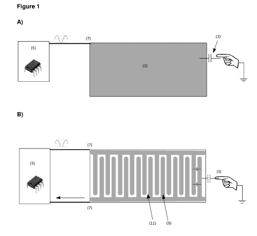
Figure 1 A) Shows a single ended capacitive sensing touch system where
capacitance
is created by a differentiated touch event (3) on the active layer (1). Any
change in capacitance travels through the node (7) to the electronic
controller
(5).
B) Shows a differential capacitive sensing touch system where capacitance
from a differentiated touch event (3) reduces capacitance. The active layer is
arranged in a pattern (9) on the substrate surface (11). Any change in
capacitance travels through the patterned active layer (9), the connecting
means (7) to the electronic controller (5) to execute a command.
Figure 2 Shows a resistive capacitive swipe touch system where the
active layer (1) is
a conductive resistive active layer. The touch event (3) in a vertical axis
(13)
provides a series of resistances (15), which travel through node (7) to the
electronic controller (5).
Figure 3 Shows an inductive touch system. The active layer (1) is
arranged as a loop
(17) on the substrate surface (11) creating a magnetic field (21). Objects
with
magnetic permeability (19) disrupt the magnetic field (23) resulting in
changes
in inductance, which are transferred via the connecting means (7) to the
controller (5).
CA 03015990 2018-08-28
WO 2017/150991
PCT/NZ2017/050022
Figure 4 Shows a closed circuit resistive system. A resistive active
layer (1b) is
arranged in a loop. A differentiated touch (3) changes the resistance of the
resistance layer (1b).
Figure 5 Shows an open circuit resistive sensing touch system. When the
circuit is
open, no current flows. A differentiated touch (3) by an object draws a
current
through the object thereby completing the electronic circuit. The current can
and measured by the electronic controller and used to issue a command.
Figure 6 Shows a possible arrangement of the active layer (1) with
other layers to form
a basic capacitive resistive coating in a sandwich type arrangement.
Figure 7 Shows a possible arrangement of the active layer (1) with
additional
electrically active layers (45) as an enhanced conductive resistive coating
basic capacitive resistive coating.
Figure 8 Shows a possible arrangement of the active layer (1) to form a
capacitive
resistive grid coating (31) and (33).
Figure 9 Shows a possible combination of active layer (1) and
electronic controller (5)
systems wireless connected and interacting with other such systems. A
computer or other Smart Phone or Tablet device may be used to remotely
connect to any of these systems, and monitor and/or configure their
behaviour.
Figure 10 Shows a touch detection algorithm during a double tap touch
event.
Figure 11 shows a touch detection algorithm during a full hand touch
followed by a
double tap touch event.
Figure 12 Shows a system with additional electrically conductive layers
in the form of
two strips. The active layer (1) comprises carbon paint and the additional
electrical conductive layers (45) are strips of copper paint along the top and
bottom of the area substrate.
26
CA 03015990 2018-08-28
WO 2017/150991
PCT/NZ2017/050022
Figure 13 Shows swipe touch events on the active layer at different
positions with
respect to two oppositely placed additional conductive layers. (47) Is a touch
nearer the bottom if the additional electrically active layer (45); (49) is a
touch
equidistant between two additional electrically active layers (45); and (51)
is a
touch close to the top of an additional electrically active layer (45).
Figure 14 Shows a possible arrangement of electronic components.
Figure 15 Shows the changes in the capacitance of the active layer, as
measured at two
additional conductive layers (45), as an object is moved toward and away
from the additional conductive layers (45) thereby signifying a swipe event.
Figure 16 Shows variation in measured capacitance caused by touches, as
a function of
distance from the connection point on a plain active layer. The active layer
is
shown diagrammatically as (1), the
connection point as 0¨ (7), and the
touch location on the active layer as = (54). The touches ((53), (55), (57),
(59),
(61), (63)) closer to the connection point provide larger capacitance
readings,
due to the resistance of the active layer.
Figure 17 Shows variation in measured capacitance ((65), (67), (69), (71),
(73), (75),
and (77)), caused by touches, as a function of distance from the connection
point when an additional electrically conductive layer is added. The active
layer is shown diagrammatically as
(1), the connection point as 0¨ (7),
and the touch location on the active layer as = (54). The measured touches
closer to the additional electrically conductive layer with the connection
point
provide larger capacitance readings.
Figure 18 Shows how signal quality may be affected by mains power
electricity in close
proximity to the coating system.
DETAILED DESCRIPTION
Definitions
Unless the context clearly requires otherwise, throughout the description and
the claims, the
words "comprise", "comprising" and the like, are to be construed in an
inclusive sense as
27
CA 03015990 2018-08-28
WO 2017/150991
PCT/NZ2017/050022
opposed to an exclusive or exhaustive sense, that is to say, in the sense of
"including, but
not limited solely to".
"Substrate" or "substrate surface" within the context of this specification is
intended to mean
the surface to which the touch system is applied to and is intended to include
at least:
interior walls; exterior walls; fences; ceilings; furniture, doors, tables,
cabinetry including
drawers, cupboards; driveways, roads, parking spaces; exterior surfaces of
vehicles
including: automotive vehicles such as cars, trucks; boats; planes. The term
'substrate has
been used herein so as to exclude substrates that are capable of rendering
electronic text
and/or electronic static or dynamic images or are in some other way
electrically active. That
is, the term 'substrate surface' excludes: handheld devices; electronic
devices such as
phones, tablets, laptops; televisions; computer monitors; and those types of
devices
intended to display electronic text and/or electronic static or dynamic
images.
As used herein, the term "active layer" is used to mean the layer that is
responsible for
activity of the touch sensitive system through an electrical property of the
active layer.
As used herein, the term "electrically inactive layers" is used to mean a
layer that has no
electrical active property.
The term "coating" as used herein is intended to mean any material that may be
applied to
the surface of an object and includes coatings such as paint applied in liquid
form, and
coatings such as wallpaper or films applied in sheet form.
The term "control" as used herein is intended to include sensing of input
signals; monitoring
of a control signal; recording of a control signal; transmission of a control
signal and/or
derivatives of the control signal between electrical devices; causing an
action(s) to be
performed in relation to the control signal being received by the controller;
or any
combination of the aforementioned. The system may be used to control any
electronic
device which requires a control signal to function. Such devices may be as
simple as one or
more light bulbs, through to one or more computers or microprocessors.
Description
The present invention relates to touch sensitive electronic systems that may
be applied to
substrates.
28
CA 03015990 2018-08-28
WO 2017/150991
PCT/NZ2017/050022
The touch sensitive systems of the present invention are able to achieve
partial or
substantial substrate surface coverage.
The touch sensitive system of the present invention comprises an active layer
(1) that may
be applied to substrates (11). In order to be active, the active layer (1) has
the capability to
provide an electrical property after application to a substrate surface
sufficient to function as
a sensor that is configured, via a suitably connected detector and/or
electronic controller, to
detect a disruption to the electrical property that is provided by the
electrically active layer.
Typically an electric current is continuously or non-continuously applied to
the active layer.
When a user touches the substrate (either the active layer directly, or a non-
active layer
above the active layer), the touch disrupts or changes an electrical property
of the active
layer, the controller being configured to detect this disruption or change.
The active layer (1) is configured to have a connecting means (7) with the
electronic
controller (5). A differentiated touch (3) on a substrate surface (11)
disrupts an electrical
property in the active layer (1). The disruption of the electrical property in
the active layer (1)
is interpreted by the electronic controller (5) to execute a command.
Electrical properties
may include: a conductive property (conductance), a resistive property
(resistance), a
resistive-capacitive property and an inductive property (induction).
The active layer (1) may include any active material that has an electrical
property that may
be disrupted. That is, the active layer (1) must be able to conduct and/or
retain some
electrical charge such that an electric property generated by the electrical
charge may be
disrupted by a person or animal directly touching the active layer, or
indirectly touching the
active layer via an intermediate non-conductive layer.
A key feature of the active layer (1) is that active layer (1) must form a 3-
dimensional
interconnected pathway over at least part of the substrate, or over different
parts of the
substrate. The 3-dimensional interconnected pathway allows for a possible
passage of an
electrical current through the active layer (1).
For example, in the case of an active layer where the electrical property of
capacitance is
detected, all conductive materials are useful to produce a capacitive coating
suitable for use
as an active layer. Where metals are incorporated into the active layer,
stability, particularly
to surface oxidation where the metal oxide is non-conductive or of low
conductivity, is an
important feature in order for the electrical property to be retained for an
extended period of
time. This may be similarly applied to resistive and inductive active
materials.
29
CA 03015990 2018-08-28
WO 2017/150991
PCT/NZ2017/050022
Electronics
The active layer (1) is connected to an electronic controller (5) through
resistive, inductive or
capacitive sensing integrated circuits and/or micro control units (MCU) by
connecting means
(7). The sensing integrated circuits and/or micro control units are capable of
sensing
changes in the electrical property of the active layer (1) when an object
disrupts the electrical
property through a differentiated touch (3). When changes in the electrical
property are
detected by the integrated circuits and/or micro control units, a control
signal being, for
example, instructions for controlling a controlling relay or a dimmer circuit
may be executed.
Those of skill in the art will readily understand that the system can be
applied to other
sensing methods and does not need to be limited to capacitive sensing,
provided that the
active layer contains the adequate active material to enable a change or
disruption to an
electrical property to be detected.
Disruptions to the electrical property may be caused by specific human or
service animal
interactions that the controller is programmed to recognise and differentiate,
such as double
tapping, triple tapping, multiple tapping, tapping and holding, sliding a
hand, arm or leg
across the surface or performing the aforementioned interactions on different
regions of the
active layer.
The electronic hardware, namely the active layer and at least a sensor or
intermediate/slave
controller connected to the active layer, are connected through a connecting
means (7). The
connecting means (7) may include a physical connecting means which connects
the master
controller to the coating, sensor or slave controller, for example over a
wired network, or
using a physical connection such as silver epoxy, conductive wires, additional
electrically
conductive layers, a screw plate, physical adhesive, conductive tape.
Alternatively the
connecting means (7) may be connected via a remote connecting means or
wireless
network that allows for commands to be executed over a wider, remote
configuration. Such
remote or wireless connecting means could include any combination of
transmitters,
receivers, transceivers, Wi-Fi and Bluetooth.
The connecting means (7) may also further comprise an intermediate connector.
Electronic hardware could be configured to be controlled over a wired or
wireless network,
via computer, mobile phone, or any other connected control device (Figure 9).
The
electronic hardware, and in particular the controller, could be networked to
other devices in
the building, so that global commands and system configuration could be
carried out.
CA 03015990 2018-08-28
WO 2017/150991
PCT/NZ2017/050022
The system may be configured to recognise particular types of contact with the
active layer
(1). For example, the electronic controller (5) could be configured, either by
predetermined
programming, or in a configuration mode used by a user of the system, to
recognise specific
gestures and to map those specific gestures to specific control
outputs/actions. Examples
include: a double tap to turn off a relay; double tap and hold (i.e. a touch
of extended
duration) to turn on locally connected relays; triple tap and hold to turn off
all lights in a
building.
.. An integrated circuit (IC) could be used for sensing, that is, for
detecting disruptions in the
electrical property of the active layer caused by touching the active layer.
The sensing IC
could be integrated with, or remote from but connected to, the controller.
The controller may include a real-time clock which could be used to control
when and at
what times an electrical appliance such as lighting for example is turned on
and off.
An external switch may be used to override the controller as a fail-safe. For
example, a
standard light switch could be retained to override the control of lighting by
the electronic
controller via the active layer.
Capacitive Sensing
The active layer and the controller may be configured to detect changes in, or
disruption to,
the capacitance of the active layer, when a current is applied to the active
layer to charge the
active layer. In the case of capacitive sensing, the active layer is connected
at one or more
points or nodes, via connecting means (7) to one or more corresponding nodes
on the
electronic controller (5) The electronic controller may optionally also be
independently
connected to an electrical earth (Figure 1A).
The electronic controller (5) determines, by suitable control algorithms and
hardware, the
capacitance of the active layer (1). For example, the electronic controller
(5) may output a
constant current into to the active layer (1). An electrical charge will flow
into the active layer
resulting in an increasing voltage over time, and voltage can be calculated
according to
equation (1):
1
(1)
C
31
CA 03015990 2018-08-28
WO 2017/150991
PCT/NZ2017/050022
Ay is voltage (volts)
I is current (amperes)
C is capacitance
At is time (seconds)
The electronic controller (5) is able to determine the capacitance by
measurement of the
voltage across the active layer (1) over a fixed time. When an object, such as
a human or
animal, touches or comes into contact with the active layer (1), the
capacitance of the active
layer will change. The electrical properties of the object (e.g. the object's
own inherent
resistance, capacitance and inductance), and the dielectric properties
(thickness and
material) between the aforementioned influence the capacitive change measured
by the
electronic controller. Any capacitance can be interpreted by the electronic
controller (5) to
issue a command or control signal.
When the active layer (1) or multiple active layers (e.g. (31) and (33)) are
configured in a grid
pattern as part of a capacitive system, it is preferred that the grid elements
are electrically
insulated from each other. That is, that there is no material capable of
electrical conductivity
between the multiple active layers. In some instances some row elements might
be
connected to other row elements or alternatively, may be connected to
other column elements. Some or all of the grid elements can be connected via
connecting
means to multiple corresponding connecting means (7) to the electronic
controller (5)
(Figure 1 B). The electronic controller (5) may also be independently
connected to an
electrical earth.
However, at this stage, the electrical circuit between the grid elements on
the conductive
active layer and the electronic controller is an open circuit.
Resistive-Capacitive Sensing
In the case of resistive-capacitive sensing, a capacitive active layer may
also have resistive
properties. The touch sensor system may be configured as a capacitive-based
position
sensor by formulating the active layer (1) to have resistive-capacitive
electrical properties.
Without wishing to be bound by theory, in the case of capacitive-resistive
sensing, the active
layer (1) may be connected by one or more connecting means (7) to the
electronic
32
CA 03015990 2018-08-28
WO 2017/150991
PCT/NZ2017/050022
controller. As seen for capacitive sensing, the electronic controller (5) may
be independently
connected to an electrical earth.
The electronic controller (5) sequentially measures the capacitance of the
active layer (1), at
each connecting means (7).
When an object, such as a human, touches to the active layer, the connecting
means (7) will
measure a change in capacitance. However, due to the series of resistance
properties of the
active layer (1), the capacitance changes measured by a single connecting
means (7)
become correspondingly smaller as the object moves further away from the
connecting
means (7).
By comparing the capacitive difference of two or more connecting means (7),
the positional
information of the object on the active layer (1) can be determined. This
positional
information is calculated by electronic controller (5) and can be used to
execute a command.
This may be further expanded to include three or more connecting means (7) to
provide
greater functionality. For example, with three connecting means (7) that are
connected along
two perpendicular edges of the active layer (1), it is possible to obtain
positional information
in horizontal and vertical axes, resulting in a 2D positional co-ordinate of
the object
disrupting the electrical property.
Inductive Sensing
The touch sensor system may also be configured as an inductive sensor by
formulating the
active layer (1) to have inductive electrical properties (Figure 3).
The active layer for the inductive sensor is also connected at one or more
connecting means
(7) to the electronic controller (5), via connecting means (7). The electronic
controller may
also optionally be independently connected to an electrical earth.
The electronic controller calculates the inductance of the inductive active
layer (17). Without
wishing to be bound by theory, the inductive active layer (17) may form part
of a resonant
resistor inductor capacitor electrical circuit when connected to the
electronic controller (5).
When the electronic controller (5) applies a short voltage pulse to the
inductive active layer
(17) (typically in the range of from about 0.1 microseconds to about 100
milliseconds), and
33
CA 03015990 2018-08-28
WO 2017/150991
PCT/NZ2017/050022
the voltage is then released, an oscillating 'ringing' voltage will result, in
which the voltage
decays over time, as a result of the resistance. The frequency of this
oscillating voltage is
known as the circuit's resonant frequency. The resonant frequency can be
measured by the
electronic controller and calculated according to equation (2):
1
fres = (2)
27tv LC
f res is resonant frequent (hertz)
L is inductance (henrys)
C is capacitance (farads)
Those of skill in the art will realise that the physical layout of the active
layer (1) influences
the amount of inductance. For example, the active layer may be arranged in a
straight line or
alternatively may form a spiral pattern or a loop (Figure 3). The length and
shape of the
active layer (1) may therefore have an effect on the amount of inductance.
It will also be understood by those of skill in the art that as an electrical
current flows through
the active layer, a magnetic field (21) is created. When a magnetically
permeable object
(19) (e.g. a metal pen/stylus) is touched against the inductive active layer
(17), the
permeability of the material will cause the inductance to change (23). This
change in
inductance, can be interpreted by the electronic controller and used to issue
a command.
Resistive Sensing
The touch sensor system may further be configured as a resistive sensor by
formulating the
active layer to have resistive electrical properties.
The active layer should be connected at two or more connecting means (7) to
the electronic
controller (5). The two or more connecting means (7) are required to provide a
complete
electrical circuit. However, one of the connecting means (7) may be an
electrical earth. At
this stage, the electrical circuit between the resistive active layer (lb) and
the electronic
controller is a closed circuit (Figure 4).
The electronic controller outputs a constant voltage across the resistive
active layer while
simultaneously measuring an electrical current through the resistive active
layer (1b). The
voltage, current and resistance are linked by way of Ohm's Law.
34
CA 03015990 2018-08-28
WO 2017/150991
PCT/NZ2017/050022
When an object, such as a human or animal, touches a portion of the resistive
active layer
(lb), it will result in a lower resistance (than resistance prior to the touch
event) and
therefore greater electrical current (than current prior to the touch event).
The increased
current, can be interpreted by the electronic controller (5), and used to
issue a command.
Ideally in a resistive system, the resistive active layer is preferably
configured as a strip
(Figure 4, (1b)).
The resistive active layer (1 b) may also be connected at a single connecting
means (7) to
the electronic controller (5). The electronic controller (5) must also be
independently
connected to an electrical earth. At this stage, the electrical circuit
between the resistive
active layer and the electronic controller (5) is an open circuit (Figure 5).
The electronic controller (5) outputs a constant voltage onto the resistive
active layer (lb)
while simultaneously measuring any electrical current that might flow through
the resistive
active layer (lb). While the electrical circuit is open, no current flows.
However, if an
electrically earthed object, such as a human or animal, touches the resistive
active layer, a
resistance will be formed between the resistive active layer (lb) and
electrical earth. An
electrical current will now be able to flow, by way of Ohm's Law, and can be
interpreted by
the electronic controller to issue a command.
Time of flight sensing
The touch control system may also be configured as part of a so called 'time
of flight' sensor.
The active layer is connected at a single connecting means (7) to the
electronic controller
(5). It is required for the electronic controller (5) to be independently
connected to an
electrical earth. However, the active layer can optionally be connected to
electrical earth via
an appropriate termination resistor. The termination resistor is
preferentially located at a
node that is the electrically farthest away node from the electronic
controller.
The time of flight sensory system works by the electronic controller (5)
outputting a short
voltage pulse onto the active layer (1) (typically between about 1 pico second
and 1 micro
second). The short voltage pulse may consist of an oscillating voltage
waveform. The
voltage pulse propagates along the active layer. However, if an object such as
a human or
animal touches the active layer (1), part of the voltage pulse will be
absorbed by the object.
Part of the pulse will then be directed back towards the electronic
controller. This
phenomenon is known as an impedance discontinuity. Once the electronic
controller (5)
CA 03015990 2018-08-28
WO 2017/150991
PCT/NZ2017/050022
senses the returned voltage pulse, the electronic controller (5) can determine
the time has
taken for the voltage pulse to travel from the electronic controller (5) to
the object and back
to the electronic controller (5). Such information can be interpreted by the
electronic
controller (5) to issue a command.
Active Layer
Conductive carbon black pigments may provide convenient and cost effective
materials for
use in the active layer. Incorporation of pigments into conventional coatings
at appropriate
levels (exceeding the concentration required to pass the percolation
threshold) produce
coatings with conductive resistive properties that are easily altered by the
type and amount
of carbon black added as well as by the state of carbon black dispersion.
Typically more
than 5 mass % of highly conductive carbon black are required to obtain
conductivity in the
active layer and more useful conductivity is afforded above 10 or 20 mass /0.
However, at
these levels the mechanical properties of the active layer become compromised
and
appropriate polymeric binding agents and formulating techniques are required
to allow
uniform film formation without cracking which leads to reduced conductivity
and worst case
no conductivity.
The active layer (1) may be applied as a coating material or alternatively the
active layer
may be covered with a coating material in a sandwich or laminate type
arrangement in
Figure 6 to Figure 8. Such coating materials may include paint formulations,
lacquers and
gels.
Touch detection
The present invention is designed to detect an intentional touch (and not a
false touch) on
the substrate surface when an object changes the capacitance of the active
layer is
disrupted. For the purpose of the present invention, false touches could be
generated by a
person or animal brushing against the substrate surface; a person or object
leaning against
the substrate surface; electrical noise sources; or random noises.
The present invention may overcome the problem of false touches by the use of
suitable
control algorithms in the electronic controller (5) (Figure 10 and Figure 11).
The control
algorithms (Figure 10 and Figure 11) are capable of detecting the number of
taps on the
surface, and/or a pattern of taps, and/or or the duration of the disruption to
the capacitance
of the active layer. The control algorithms may therefore distinguish between
a single touch
36
CA 03015990 2018-08-28
WO 2017/150991
PCT/NZ2017/050022
or tap of short duration, which might be a false touch which is not intended
to generate a
control signal, from a true touch, which is intended to generate a control
signal. The control
algorithms do this by dismissing any single touch below a predetermined
duration, or below
a predetermined measure of disruption of the electric property.
The control algorithms also work with low signal to noise environments, and
also work well to
filter out noise associated with a slow increase or decrease of offset
capacitance such as
might occur when a user leans against a wall or touches the wall while also
tapping.
It has been found by the present inventors that two or more tap events are
more likely to
remove false touch events than a single tap or touch. This therefore, provides
improved
reliability that the disruption of the capacitance is a result of an
intentional, true touch event,
rather than false touch event disruption. True touch events may incorporate a
number of
touches and/or a measure of for how long the touch event has occurred. This
allows for the
detection of multiple tap events, tap and hold events as different commands,
and allows the
control algorithms to provide, and distinguish between, a number of different
commands.
A control algorithm processes the input data (35) and (41), as shown in Figure
10 and
Figure 11, to create edge detection data (37) and (43). An edge detection
algorithm
compares this to a threshold to set the current state (34) and (42) to one of
3 states: Touch
On (value = 1), Touch Off (value = -1), or No Touch (value = 0). Data is then
fed into a
decision tree along with current time to count the number of touch events that
have occurred
((39) and (44)). Once no touches have been detected for a set time, the final
count of
occurred touches is recorded and a touch event generated.
The control algorithm may be able to process, recognise, and generate
particular outputs in
response to, multiple different gestures. The gestures may differ in the
number of taps and
holds, and/or the duration of the taps and holds. The controller may be
configured such that
each gesture generates a corresponding control action such as turning on
lights, changing
dimming settings, or turning off all lights in a particular area of a
building.
The present invention may also incorporate gestures such as a swipe event
where
functionality is similar to a slider used to control domestic electrical
appliances. Swipe
events open up the number of options available as input signals and commands.
Swipe
events could be used to control activities in the home such as dimming lights
or other
indications. Further, swipe events on the substrate surface may be implemented
by
incorporating a two layer system together with two additional electrically
conductive layers,
37
CA 03015990 2018-08-28
WO 2017/150991
PCT/NZ2017/050022
having an area that is less than the area of the active layer in the form of
strips or channels
(e.g. as shown in Figure 1B, Figure 3, Figure 8). One, two or more channels of
additional
electrically conductive material may be used for this purpose as shown in
(Figure 8).
In one example, the swipe event is implemented on a wall with a two layer
system having an
active layer (such as conductive carbon paint), and additional electrically
conductive areas
(such as copper paint) (45) in the form of horizontal strips, located on the
upper and lower
edges of the active layers (Figure 12). The capacitance measured at each
respective
additional conductive strip is inversely proportional to the distance between
the additional
conductive strip and the touch location; the difference in measured
capacitance at each
additional conductive strip allows for calculation of the touch location.
Figure 13 shows five distinct touches; the three in the centre signify touches
equidistant
from the additional electrically conductive layers (45). The first touch (47)
is closer to one
additional electrically conductive layer (45), while the last touch (51) is
closer to the other
additional electrically conductive layer (45).
Arrangement of the active layer
The active layer (1) may be applied under and/or on top of other layers (25),
(27), (45).
Other layers may be selected from primers/sealers (25), additional
electrically active layers
(45), topcoats (27), and base layers (25).
It is also possible to have more than one active layer on a substrate surface.
When there is
more than one active layer, the active layers may be sandwiched between a non-
conductive
layer (30). The layers may be arranged, for example, as shown in Figure 6 to
Figure 8.
Those of skill in the art will realise that the layers may have alternative
arrangements to
those shown herein.
Where the active layer (1) is used in conjunction with additional electrically
conductive layers
(45), the additional electrically conductive layers may be arranged as strips
or bands on the
periphery of the active layer (1) as shown in Figure 12. Alternatively, the
additional
electrically conductive layer (45) may also be arranged in vertical or
horizontal series as
shown in Figure 8. An important feature is that the electric property
generated by current
passing through the layers may still be disrupted by a manual touch event. In
other words,
the arrangement of conductive elements in the active layer (1) is such that
disruptions to the
selected electric property of the active layer may be detected by the
controller. The change
38
CA 03015990 2018-08-28
WO 2017/150991
PCT/NZ2017/050022
or disruption in electric property may be generated from a passive electric
field in that the
coating may not require an active power source as such. With a controller of
suitable
sensitivity, a relatively small disruption in the passive electric property
caused by the touch of
a user may be detected without electricity being supplied to the active
coating.
The additional electrically conductive layer may take the form of a horizontal
strip derived
from a conductive material such as copper paint or similar between the sliding
points.
The capacitance measured at each respective additional conductive layer is
inversely
proportional to the distance between the additional conductive layer and the
touch location;
the difference in measured capacitance at each additional conductive layer
allows for
calculation of the touch location.
A problem of some prior art systems is that low cost conductive paints used
for an active
layer have high resistance, which also means that they have low conductance.
Therefore,
the capacitive signal of the active layer is smaller, the further away the
touch occurs from the
controller.
The present invention solves the problem by using an additional electrically
conductive layer
and/or a connecting means. The additional electrically conductive layer (45)
and/or a
connecting means (7) must have lower resistance and higher conductivity than
the active
layer. The higher conductivity prevents the signal from dropping off or
diminishing in
intensity, and may be seen in Figure 16.
The present inventors also found that some of the prior art system were
problematic when
applied to larger substrates. Mains electricity supply in close proximity to a
coating system,
increased the amount of noise observed, which in turn affected the noise to
signal ratio
making it harder for a touch event to be detected by the controller when the
capacitance was
disrupted. The present inventors have established that synchronising the
measurements
(resistance and/or capacitance and/or inductive measurements) of the
conductive active
layer by the electronic controller with the same frequency of the mains
electrical supply may
avoid the problem of electrical noise (see Figure 18).
It will be appreciated that the above described touch sensitive system may
find application
anywhere where touching an otherwise passive substrate could be used to
control an
electrical device. Such appliance device might be a light for example, or
might be an alarm,
or might be a motor or other electrical actuator used to move an object such
as a door or
39
CA 03015990 2018-08-28
WO 2017/150991
PCT/NZ2017/050022
gate or lock, or a relay which is used to connect a circuit to control an
electrical appliance.
Further, more detailed examples have been provided above.
The following provides two non-limiting example compositions for forming an
active layer in
accordance with the current invention:
General Procedure A:
With mixing, a 20% portion of water was added to 25% of an alkali soluble
dispersion
followed by 25% of alkali. The mixture was stirred until a clear solution was
obtained. With
continued mixing, the surfactant, propylene glycol and defoamer were added and
the mixture
stirred under high shear conditions (e.g. high speed mixer with a cowles
blade) while carbon
black powder was slowly added in portions. Viscosity was adjusted by portion-
wise addition
of water until a paste was produced. The paste was further processed to break
agglomerates and produce a fine dispersion. A fine dispersion was achieved by
additional
processing methods by adjusting the viscosity with a further 50% of the total
water and, after
transferring the mixture to a round vessel, adding zirconia dispersion beads
and subjecting
the vessel to rotation by placing the vessel on a roller for several days.
After the additional
processing, the dispersion beads were removed by filtration and the remaining
water, alkali
soluble acrylic dispersion, alkali and biocide were added. After thoroughly
mixing all
components to a homogeneous state the material was ready for use.
Material Type Supply Name
Mass %
Surfactant Genapol 0 080 (EFKA) 0.5
Propylene Glycol 5.5
Defoamer Foamstar SI 2250 (BASF) 0.3
Conductive carbon powder Printex XE2B (Orion Engineered Carbon) 5.5
Alkali Soluble acrylic Viscopol 7396 (Nuplex) or Primal 1-98 (Dow)
17.4
dispersion (solid component)
Water
67.2
Biocide Acticide MBS (Thor) 0.1
Alkali 10% aq. Alkali hydroxide or 25% aqueous 3.4
ammonia
100
General Procedure B:
CA 03015990 2018-08-28
WO 2017/150991
PCT/NZ2017/050022
To the alkali soluble acrylic dispersion was added 50% of the total water,
alkali, wetting
agent, defoamer and rheology modifier. The mixture was stirred until all
rheology modifier
had dissolved. Conductive metal powders were added while stirring and after
complete
wetting of the powders the remaining water and biocide were added. After
mixing to a
homogeneous state the coating was ready for use.
Material Type Supply Name
Mass %
Alkali Soluble acrylic Viscopol 7396 (Nuplex) or Primal 1-98 (Dow)
11.4
dispersion (solid component)
Water
66.9
Biocide Acticide MBS (Thor) 0
Alkali 10% aq. Alkali hydroxide or 25% aqueous 0.4
ammonia
Defoamer Foamstar SI 2250 (BASF) 1.0
Wetting agent Surfynol 104DPM (Air Products) 0.8
Rheology modifier Natrosol PLUS D330 (Ashland) 0.4
Conductive metal powder eConduct 421000 (Eckart) 3.8
Conductive metal powder eConduct 122000 (Eckart)
15.3
41